基于CH3NH3PbI3单晶的Ta2O5顶栅双极性场效应晶体管
2017-03-13 09:53吕乾睿廉志鹏赵昊岩董桂芳王立铎严清峰
物理化学学报 2017年1期
吕乾睿 李 晶 廉志鹏 赵昊岩 董桂芳 李 强 王立铎 严清峰
(清华大学化学系,北京100084)
基于CH3NH3PbI3单晶的Ta2O5顶栅双极性场效应晶体管
吕乾睿 李 晶 廉志鹏 赵昊岩 董桂芳*李 强 王立铎 严清峰*
(清华大学化学系,北京100084)
具有无机-有机杂化钙钛矿结构的CH3NH3PbI3通常偏向于显示n型半导体特性,本文以五氧化二钽(Ta2O5)作为绝缘层,制备了基于钙钛矿CH3NH3PbI3单晶的顶栅结构场效应晶体管,暗态下更明显地观察到了CH3NH3PbI3所具有的p型场效应特性,空穴场效应迁移率达到8.7×10⁻⁵cm2·V-1·s-1,此暗态空穴迁移率比原有报道的基于CH3NH3PbI3多晶薄膜的SiO2底栅场效应晶体管提高了一个数量级。此外,光照对CH3NH3PbI3单晶场效应晶体管的性能有强烈影响。与底栅结构CH3NH3PbI3多晶场效应晶体管不同,即使有栅极和绝缘层的遮挡,5.00 mW·cm-2的光照仍可使CH3NH3PbI3单晶场效应晶体管的空穴电流提高一个数量级(VGS(栅源电压)=VDS(漏源电压)=20 V),光响应度达到2.5 A·W-1。本文工作实现了对CH3NH3PbI3场效应晶体管载流子传输的选择性调控,表明在没有外部因素的参与下,通过合适的器件设计,CH3NH3PbI3同样具有制备成双极性晶体管的潜力。
钙钛矿;五氧化二钽;场效应;迁移率;光照
1 Introduction
Methyl ammonium lead iodide(CH3NH3PbI3,MAPbI3)based organic-inorganic hybrid perovskites have attracted much attention in recent years because of their rapid progress in solar cell1-5, light-emitting diodes6,7,memristor8,photodetectors9,etc.Their excellent properties have been ascribed to the appropriate direct band gap10,large absorption coefficient11,long-range balanced electron-and hole-transport lengths12,and high electrical mobility13of the perovskites.In addition,MAPbI3exhibits ambipolar property14,which provides more possibilities for the application in the field of electronic and optoelectronic devices15.Although MAPbI3have achieved tremendous progress in practical application,physical properties of this material,for example the chargetransport mechanisms are still not fully understood16.Field-effect transistors(FETs)are important electrical devices and also have been extensively used to explore the carrier transport characteristics in semiconductor materials.From this point of view,the study on MAPbI3FETs is of paramount importance to deepen the understanding of carrier transport characteristics in MAPbI3material.
At present,the reported MAPbI3FETs are all based on polycrystalline film and their performances in the dark are still below expectations17-19.Aconsensus is that the low hole mobility(~10-6cm2·V-1·s-1)resulted from the screening effect has impeded the progress of their FET applications17,18.Therefore,improving the FET mobility of MAPbI3,especially the hole mobility,is of great importance to promote the FET application.Chin et al.18reported that increased field-effect carrier mobility by almost two orders of magnitude could be achieved below 200 K,because lowering the operating temperature could effectively eliminate the screening effects.Li et al.19suggested that there was no obvious field effect in MAPbI3polycrystalline film in the dark and the field effect could only be induced under light illumination with the help of the photo-induced carriers.Overall,up to date,in order to observe field effect in the MAPbI3polycrystalline film,appropriate external factor should be applied.Furthermore,as to ambipolar materials,for integrating both devices with p-and n-type conductions on the same material,selectively but not equally regulating the hole or electron transport in FETs according to the actual needs is important20.Unfortunately,the external factors mentioned above resulted in leveling the transport of electron and hole in the same time18.
In this paper,we report a top-gate FET device based on singlecrystal MAPbI3with Ta2O5as the gate dielectric.Without external factors,we not only observed field effect in the single-crystal MAPbI3transistor,but also achieved selective regulation of the hole mobility.Compared with the polycrystalline MAPbI3,the field effect was more obvious and the hole mobility increased by one order of magnitude at room temperature.These results were significant in the physical property understanding and the application developing of MAPbI3materials.
2 Experimental
2.1 Preparation and structural characterization of perovskite MAPbI3single crystal
The growth of MAPbI3single crystal was based on the method described by Poglitsch and Weber21.All chemicals were used as received without further purification.Pb(CH3COOH)2·3H2O (99.5%)from Sinopharm Chemical Reagent Co.,Ltd.,China.57% HI aqueous solution with 0.75%H3PO2as stabilizer was from Acros,USA and 40%CH3NH2aqueous solution was from Alfa. 7.5 g of Pb(CH3COOH)2·3H2O was dissolved in 30 mL of a 57% HI aqueous solution contained in a Erlenmeyer flask under stirring condition in air.The Erlenmeyer flask was put on a heating plate (Ika C-MAG)and slightly heated to make them dissolve sufficiently and quickly,till the solution turned homogeneous bright yellow.An additional pre-made 6 mL of 57%HI solution with 2 mL of CH3NH240%aqueous solution was added to the solution drop by drop at about 373 K to ensure no black solid appear.The Erlenmeyer flask was put into an oven after sealing.Black single crystals were grown at the bottom of the Erlenmeyer flask by cooling this yellow solution to 333 K in 10 days.After filtered and dried at 333 K in vacuum oven for 12 h,the crystals were collected for structural characterization and device fabrication.The as-grown MAPbI3single crystals were oriented by X-ray crystal diffraction(XRD)instrument(Brüker P4)using Cu Kαradiation at a scan rate of 12(°)·min-1under operation condition of 40 kV and 40 mA.To ensure that the single crystals belong to a pure phase,several crystals were ground to powder and the powder XRD data were collected in the same test conditions.The absorption spectrum was collected on a Perkin Elmer Lambda 950 spectrophotometer.The surface morphology of as-grown MAPbI3single crystals was characterized using an atomic force microscope(AFM,Seiko instrument SPA400).
2.2 FET device fabrication and characterization
A fresh MAPbI3single crystal(3 mm×3 mm×1.5 mm)with flat surface was chosen to fabricate the FET.Au strips of 70 nm in thickness were deposited on the upper flat surface of the single crystal by a conventional thermal evaporation method through a stainless steel mask as source electrodes and drain electrodes.The deposition rate was 0.01 nm·s-1and it was suspended several times during the process to protect the single crystal from overheating.The channel width(W)was 800 μm,and the channel length(L)was 50 μm.Ta2O5dielectric layer with a thickness of 300 nm was deposited on the MAPbI3single crystal with source electrodes and drain electrodes by magnetron reactive sputteringin an Ar/O2(1:1(volume ratio))gas mixture.The gate electrode was Au strip,with the same deposition process of the source electrodes and drain electrodes.Au wires were led from three electrodes to facilitate FET testing.By changing the gate-source voltage(VGS)and monitoring the drain-source current(IDS)under different drain-source voltage(VDS),the field-effect was characterized.The output and transfer curves of the FET were measured using a semiconductor characterization system(Keithley 4200) under ambient conditions.The experiment light was from fluorescent lamps and solar simulators(Thermo oriel 91192-1000).The FET was illuminated from the Au gate to the MAPbI3single crystal.

Fig.1 (a)Photograph of an as-grown MAPbI3single crystal,(b)XRD patterns of MAPbI3single crystal and its powder, (c)atomic force microscope(AFM)height image and(d)the corresponding three-dimensional topographic image of a MAPbI3single crystal
3 Results and discussion
A MAPbI3single crystal of~3 mm×3 mm×1.5 mm in dimension is shown in Fig.1(a).The obvious mirror-like surfaces indicate that the crystal tends to exhibit their natural rhombic and parallelogram facets.As shown in Fig.1(b),the diffraction signal of the top facet of the single crystal contains only two sharp peaks, which is identified to be the(200)and(400)diffractions.Thus,the top natural facet of the crystal was determined to be(100).The orientation result matches with previous report22.The powder X-ray diffraction patterns of the ground crystals demonstrate a classic tetragonal perovskite structure,which is in good agreement with the patterns of MAPbI3polycrystalline films23.The absorption spectrum is shown in Fig.S1(Supporting Information),which confirms the 1.49 eV bulk band gap.More detailed structural and optical characterization of the as-grown single crystals can be found in our previous report24.Furthermore,as shown in Fig.1(c) and Fig.1(d),the single crystal surface displays a root-meansquare roughness of 1.36 nm in a typical scanning area of 5 μm× 5 μm,which is far lower than that of usual MAPbI3polycrystalline films19.There are some circular holes on the single crystal surface, which might be caused by the erosion from the residual growth solution during the post-growth treatment.
A FET with the top-gate structure as schematically shown in Fig.2(a)was fabricated on the(100)facet of the MAPbI3single crystal.Each layer constituting the FET can be clearly observed under the optical microscope(Fig.2(b)).Fig.3 shows FET characteristics of the device.The hole transport properties are presented in Fig.3(a)and Fig.3(c)while Fig.3(b)and Fig.3(d)reflect the electron transport properties.The field effect can be observed, indicating that both electrons and holes could be induced as charge carriers under electric field.This result is in accordance with the ambipolar transport property as previously reported in polycrystalline films18.The IDSis higher than that in polycrystalline films.It is worth noting that the field effect could be observed in the dark condition in a MAPbI3single crystal,which was barely observed in the MAPbI3polycrystalline film18,19.In the polycrystalline film,the grain boundary gives rise to a large concentration of traps or ion vacancies and the screen effect is remarkable.These factors overshadowed the field effect of its own.Previous study has shown that the perovksite film having fewer grain boundaries and thus less ion vacancies resulted in smaller ion drift velocity25.Considering that single crystals can decrease the concentration of traps or ion vacancies and eliminate the screening effect to the greatest extent because of the absence of grain boundaries,it is expected that the single-crystal FET may reflect the intrinsic property of MAPbI3.That′s also why one may observe the field effect even in the dark condition in a MAPbI3single crystal FET.It should be noted that a lot of destructive testing experiments showed that the IDSreached saturation quickly, and the saturation region of the FET was very short,which could be ascribed to the high permittivity of Ta2O5.When the VDSreached about 25 V,the FETs went into the breakdown region and the device was destroyed(see Fig.S2,Supporting Information).The field-effect mobility(μ)of the FET device was calculated through the slope in the linear region in the transfer curve(Fig.3(c,d))by using the following equation:

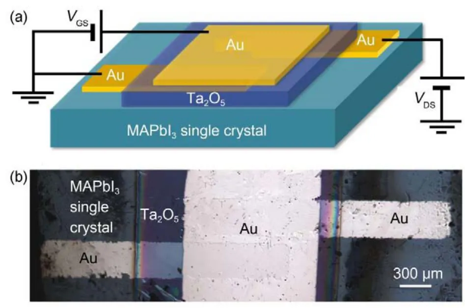
Fig.2 (a)Sketch and(b)optical microscope image of the FET based on a MAPbI3single crystal

Fig.3 FET characteristics of MAPbI3single crystal
where Ci(6.6×10⁻⁸F·cm-2)is the unit area capacitance of the Ta2O5dielectric layer,which is from our previous experimental data26.The mobility extracted from transfer characteristics in the dark is 8.7×10⁻⁵cm2·V-1·s-1for holes and 2.6×10⁻⁵cm2·V-1· s-1for electrons,respectively.The hole mobility in the single crystal is more than 3 times than the electron mobility.Compared with the MAPbI3polycrystalline film,the field effect is more obvious and the hole mobility increases by one order of magnitude than that in polycrystalline FETs at room temperature.The on/off current ratio is less than 2.Although this on/off current ratio in the dark is much lower than conventional FETs such as Si/Ge FET,it is a breakthrough for this perovskite material because the field effect in the dark was difficult to be observed in previously reported MAPbI3polycrystalline film FET because of the lack of movable carriers.In addition,in MAPbI3polycrystalline film FET with SiO2as the gate dielectric,the electron mobility was larger than the hole mobility18,while in the bulk crystals with Ta2O5as the gate dielectric,the holes were more easily transported than theelectrons.This result might be caused by the electron trapping sites from the vacant Ta orbits in Ta2O5,which could serve as electron acceptors26,27.As a result,the transport of holes was enhanced.It is expected that by selecting a suitable insulating layer or gate patterning,p-channel or other custom-made MAPbI3FET may be achieved,which will help the device integration to a large extent.Further improving the contact conditions and the quality of the crystal surface may dramatically improve the carrier mobility and on/off current ratio,which is worthy of study in the future.
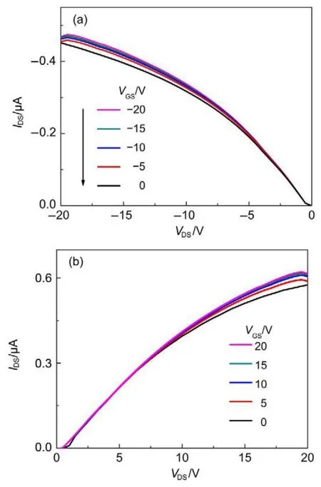
Fig.4 Output characteristics of the FET under the fluorescent lamp condition
To further validate this conjecture,the effect of light illumination on the MAPbI3single crystal FET was also studied.The output characteristic curves of electrons and holes under a fluorescent lamp were shown in Fig.4.The power density was 0.04 mW·cm-2,which was far lower than that required by a MAPbI3polycrystalline film phototransistor19.In addition,the light illumination was shielded by the top gate dielectric compared with the bottom gate dielectric FETs.Even if under this condition,the improvement in IDScould be observed.However,the regulatory capacity of VGSto IDSdropped significantly,which means that when MAPbI3single crystal FET was illuminated with weak light,the light stimulated more carriers and the photon-generated carrier exhibited directional movement under the electric field.In this top gate transistor,the photo-generated carrier concentration was too large and the gate-modulated IDSwas only a little part of the photogenerated IDS.This large amount of photo-generated carrier was owe to the photoelectric response of the MAPbI3single crystal.In other words,the carrier concentration and the transport ability of the single crystal could be obviously enhanced without requiring strong illumination.These results further confirmed the MAPbI3single-crystal FET had higher responsivity compared to the FETs based on MAPbI3polycrystalline film.When the power density increased to 5.00 mW·cm-2by a solar simulator,IDSwas further increased.It increased by one order of magnitude than that in the dark(VGS=VDS=20 V)and the photo responsivity reached 2.5A· W-1.The output curves tended to straight lines and almost coincided(Fig.5).

Fig.5 Output characteristics of the FET under the solar simulator condition
To further illustrate the importance of the selection of the device structure and the dielectric layer material in the single-crystal FET, a FET device with a bottom-gate/top-contact structure based on single-crystal MAPbI3is shown in Fig.S3(Supporting Information),in which 300 nm thick thermally oxidized SiO2was applied as the dielectric layer.The single crystal with source electrodes and drain electrodes was pressed onto the Si/SiO2substrate gently to form the FET(see Fig.S3).The FET characterization showed that to observe the field effect,a greater VDSand VGSshould be applied and the IDSjitters during the testing(see Fig.S4,Supporting Information).Except for the lower permittivity of SiO2,we owned this result to the super long carrier transport length(1.5 mm,the thickness of the single crystal)from the drain electrode to the channel,then to the source electrode and more importantly the poor interface between the channel and the insulating SiO2.It isworth mentioning that in this FET with SiO2as the insulating layer,electrons showed stronger transport ability than holes.The mobility extracted from transfer characteristics is 0.0024 cm2·V-1· s-1for holes and 0.17 cm2·V-1·s-1for electrons.
4 Conclusions
In summary,MAPbI3single crystals were successfully grown by a temperature-lowering solution growth method.A prototype FET device based on the single crystal MAPbI3and the Ta2O5as the top gate dielectric layer was made and its field-effect characteristics were observed in the dark.The ambipolar transport characteristic was found in single-crystal MAPbI3FETs.The hole transport was selectively enhanced because of the large amount of electron trapping sites in Ta2O5.In the top gate transistor,faint light could make the field effect disappear and make the IDSincrease sharply because of the high responsivity of MAPbI3single crystals.The higher FET hole mobility in single-crystal organicinorganic hybrid perovskite may further stimulate the integration and application of these materials in electronic and optoelectronic devices.
Supporting Information:available free of charge via the internet at http://www.whxb.pku.edu.cn.
(1)Kim,H.S.;Lee,C.R.;Im,J.H.;Lee,K.B.;Moehl,T.; Marchioro,A.;Moon,S.J.;Humphry-Baker,R.;Yum,J.H.; Moser,J.E.Sci.Rep.2012,2,591.doi:10.1038/srep00591
(2)Etgar,L.;Gao,P.;Xue,Z.;Peng,Q.;Chandiran,A.K.;Liu,B.; Nazeeruddin,M.K.;Grätzel,M.J.Am.Chem.Soc.2012,134, 17396.doi:10.1021/ja307789s
(3)Burschka,J.;Pellet,N.;Moon,S.J.;Humphry-Baker,R.;Gao, P.;Nazeeruddin,M.K.;Grätzel,M.Nature 2013,499,316. doi:10.1038/nature12340
(4)Liu,M.;Johnston,M.B.;Snaith,H.J.Nature 2013,501,395. doi:10.1038/nature12509
(5)Zhou,H.;Chen,Q.;Li,G.;Luo,S.;Song,T.B.;Duan,H.S.; Hong,Z.;You,J.;Liu,Y.;Yang,Y.Science 2014,345,542. doi:10.1126/science.1254050
(6)Xiao,J.;Zhang,H.L.Acta Phys.-Chim.Sin.2016,32,1894. [肖 娟,张浩力.物理化学学报,2016,32,1894.]doi:10.3866/ PKU.WHXB201605034
(7)Tan,Z.K.;Moghaddam,R.S.;Lai,M.L.;Docampo,P.;Higler, R.;Deschler,F.;Price,M.;Sadhanala,A.;Pazos,L.M.; Credgington,D.Nat.Nanotech.2014,9,687.doi:10.1038/ nnano.2014.149
(8)Yan,K.;Peng,M.;Yu,X.;Cai,X.;Chen,S.;Hu,H.;Chen,B.; Gao,X.;Dong,B.;Zou,D.J.Mater.Chem.C 2016,4,1375. doi:10.1039/C6TC00141F
(9)Fang,H.;Li,Q.;Ding,J.;Li,N.;Tian,H.;Zhang,L.;Ren,T.; Dai,J.;Wang,L.;Yan,Q.J.Mater.Chem.C 2016,4,630. doi:10.1039/C5TC03342J
(10)Lee,M.M.;Teuscher,J.;Miyasaka,T.;Murakami,T.N.; Snaith,H.J.Science 2012,338,643.doi:10.1126/ science.1228604
(11)De Wolf,S.;Holovsky,J.;Moon,S.J.;Löper,P.;Niesen,B.; Ledinsky,M.;Haug,F.J.;Yum,J.H.;Ballif,C.J.Phys.Chem. Lett.2014,5,1035.doi:10.1021/jz500279b
(12)Xing,G.;Mathews,N.;Sun,S.;Lim,S.S.;Lam,Y.M.;Grätzel, M.;Mhaisalkar,S.;Sum,T.C.Science 2013,342,344. doi:10.1126/science.1243167
(13)Stoumpos,C.C.;Malliakas,C.D.;Kanatzidis,M.G.Inorg. Chem.2013,52,9019.doi:10.1021/ic401215x
(14)Giorgi,G.;Fujisawa,J.I.;Segawa,H.;Yamashita,K.J.Phys. Chem.Lett.2013,4,4213.doi:10.1021/jz4023865
(15)Grätzel,M.Nat.Mater.2014,13,838.doi:10.1038/nmat4065
(16)Sum,T.C.;Mathews,N.Energy Environ.Sci.2014,7,2518. doi:10.1039/c4ee00673a
(17)Heo,J.H.;Im,S.H.;Noh,J.H.;Mandal,T.N.;Lim,C.S.; Chang,J.A.;Lee,Y.H.;Kim,H.J.;Sarkar,A.;Nazeeruddin, M.K.Nat.Photonics 2013,7,486.doi:10.1038/ nphoton.2013.80
(18)Chin,X.Y.;Cortecchia,D.;Yin,J.;Bruno,A.;Soci,C.Nat. Commun.2015,6,7383.doi:10.1038/ncomms8383
(19)Li,F.;Ma,C.;Wang,H.;Hu,W.;Yu,W.;Sheikh,A.D.;Wu,T. Nat.Commun.2015,6,8238.doi:10.1038/ncomms9238
(20)Shokouh,S.H.H.;Jeon,P.J.;Pezeshki,A.;Choi,K.;Lee,H. S.;Kim,J.S.;Park,E.Y.;Im,S.Adv.Funct.Mater.2015,25, 7208.doi:10.1002/adfm.201502008
(21)Poglitsch,A.;Weber,D.J.Chem.Phys.1987,87,6373. doi:10.1063/1.453467
(22)Dang,Y.;Liu,Y.;Sun,Y.;Yuan,D.;Liu,X.;Lu,W.;Liu,G.; Xia,H.;Tao,X.CrystEngComm 2015,17,665.doi:10.1039/ C4CE02106A
(23)Im,J.H.;Lee,C.R.;Lee,J.W.;Park,S.W.;Park,N.G. Nanoscale 2011,3,4088.doi:10.1039/c1nr10867k
(24)Lian,Z.;Yan,Q.;Lv,Q.;Wang,Y.;Liu,L.;Zhang,L.;Pan,S.; Li,Q.;Wang,L.;Sun,J.L.Sci.Rep.2015,5,16563. doi:10.1038/srep16563
(25)Xiao,Z.;Yuan,Y.;Shao,Y.;Wang,Q.;Dong,Q.;Bi,C.; Sharma,P.;Gruverman,A.;Huang,J.Nat.Mater.2015,14,193. doi:10.1038/NMAT4150
(26)Liu,X.;Zhao,H.;Dong,G.;Duan,L.;Li,D.;Wang,L.;Qiu,Y. ACS Appl.Mater.Interfaces 2014,6,8337.doi:10.1021/ am501197d
(27)Liang,Y.;Dong,G.;Hu,Y.;Wang,L.;Qiu,Y.Appl.Phys.Lett. 2005,86,132101.doi:10.1063/1.1896099
CH3NH3PbI3Single Crystal-Based Ambipolar Field-Effect Transistor with Ta2O5as the Top Gate Dielectric
LÜ Qian-Rui LI Jing LIAN Zhi-Peng ZHAO Hao-Yan DONG Gui-Fang*LI Qiang WANG Li-Duo YAN Qing-Feng*
(Department of Chemistry,Tsinghua University,Beijing 100084,P.R.China)
Organic-inorganic hybrid perovskite methylammonium lead iodide(CH3NH3PbI3)generally tends to show n-type semiconductor properties.In this work,a field-effect transistor(FET)device based on a CH3NH3PbI3single crystal with tantalum pentoxide(Ta2O5)as the top gate dielectric was fabricated.The p-type field-effect transport properties of the device were observed in the dark.The hole mobility of the device extracted from transfer characteristics in the dark was 8.7×10⁻⁵cm2·V-1·s-1,which is one order of magnitude higher than that of polycrystalline FETs with SiO2as the bottom gate dielectric.In addition,the effect of light illumination on the CH3NH3PbI3single-crystal FET was studied.Light illumination strongly influenced the field effect of the device because of the intense photoelectric response of the CH3NH3PbI3single crystal.Different from a CH3NH3PbI3polycrystalline FET with a bottom gate dielectric,even with the top gate dielectric shielding, light illumination of 5.00 mW·cm-2caused the hole current to increase by one order of magnitude compared with that in the dark(VGS(gate-source voltage)=VDS(drain-source voltage)=20 V)and the photoresponsivity reached 2.5 A·W-1.The introduction of Ta2O5as the top gate dielectric selectively enhanced hole transport inthe single-crystal FET,indicating that in the absence of external factors,by appropriate device design, CH3NH3PbI3also has potential for use in ambipolar transistors.
Perovskite;Tantalum pentoxide;Field-effect;Mobility;Light illumination
O649
icle]
10.3866/PKU.WHXB201610142www.whxb.pku.edu.cn
Received:August 22,2016;Revised:October 14,2016;Published online:October 14,2016.
*Corresponding authors.DONG Gui-Fang,Email:donggf@mail.tsinghua.edu.cn;Tel:+86-10-62782287.
YAN Qing-Feng,Email:yanqf@mail.tsinghua.edu.cn;Tel:+86-10-62792830.
The project was supported by the National Natural Science Foundation of China(51173097,91333109),National Key Basic Research Program of China(2013CB632900),Tsinghua University Initiative Scientific Research Program,China(20131089202,20161080165),and Open Research Fund Program of the State Key Laboratory of Low-Dimensional Quantum Physics,China(KF201516).
国家自然科学基金(51173097,91333109),国家重点基础研究发展规划项目(2013CB632900),清华大学自主科研项目(20131089202,
20161080165)和低维量子物理国家重点实验室开放基金(KF201516)资助
©Editorial office ofActa Physico-Chimica Sinica
猜你喜欢
科学导报(2022年17期)2022-04-02
大自然探索(2021年7期)2021-09-26
西安电子科技大学学报(2019年4期)2019-08-20
电子制作(2019年11期)2019-07-04
戏剧之家(2017年10期)2017-06-21
浙江大学学报(工学版)(2016年2期)2016-06-05
烟草科技(2015年8期)2015-12-20
高等建筑教育(2015年1期)2015-03-12
郑州大学学报(医学版)(2015年1期)2015-02-27
国外科技新书评介(2014年6期)2014-12-17