
Magnetotransport properties of graphene layers decorated with colloid quantum dots∗
2019-06-18 05:42RiJiaZhu朱日佳YuQingHuang黄雨青JiaYuLi李佳玉NingKang康宁andHongQiXu徐洪起
Chinese Physics B 2019年6期
关键词:康宁
Ri-Jia Zhu(朱日佳),Yu-Qing Huang(黄雨青),Jia-Yu Li(李佳玉),Ning Kang(康宁),‡,and Hong-Qi Xu(徐洪起)1,,3,§
1School of Physics,Dalian University of Technology,Dalian 116024,China
2Beijing Key Laboratory of Quantum Devices,Key Laboratory for Physics and Chemistry of Nanodevices and Department of Electronics,Peking University,Beijing 100871,China
3Division of Solid State Physics,Lund University,P.O.Box 118,S-22100 Lund,Sweden
Keywords:graphene,colloid quantum dots,quantum Hall effect,Aharonov-Bohm oscillations
1.Introduction
The quantum oscillations in solid state devices,caused by the wave character of the transport carriers, are not only important for providing the fundamental understanding of the exotic quantum phase but also the underlying mechanism for novel devices,such as electron interferometers,resonators,etc.[1-5]It has been shown that graphene,a two-dimensional(2D)electronsystem made from a single sheet of carbon atoms arranged in a hexagonal lattice,represents an ideal system to study the quantum interference effect.This is,on one hand,due to the superior electrical qualities of graphene layers such that ultrahigh mobility and long coherence length can be achieved.[6-9]On the other hand,the unique dispersion relation of graphene is analogue to that from the massless relativistic particles,which adds new aspect to the interferometric spectrum.[10-12]One of the important consequences of this 2D material is that the carrier transport in graphene is less screened and electrical properties of graphene devices are sensitive to the surrounding environment and impurities.[9,13,14]It has been demonstrated that decoration of the graphene devices with metallic nanoparticles,semiconductor quantum dots,functionalized molecules,etc.can strongly influence the electrical,magnetic,and optoelectronic properties of the devices that may lead to potential innovations for superconducting materials,spintronics,photodetectors,as well as sensing applications.[15-21]
In the present work,we study the magnetotransport properties of bilayer graphene devices decorated with PbS colloid quantum dots(CQDs).The low temperature magnetoconductance measurement in such hybrid devices displays robust Aharonov-Bohm(AB)type oscillations in both weak and strong magnetic field regimes,providing evidence for the scattering potential introduced by the CQDs.The lateral size of the scattering potential is estimated from the quantum oscillations.These experimental findings demonstrate that the hybrid CQDs/graphene devices provide a flexible system for studying the quantum interference effect in 2D material systems that are sensitive to the electrostatic environment.
2.Experiment
The hybrid CQDs/graphene device structure in the present study is shown schematically in Fig.1.The device is composed of graphene field effect transistors(FETs)and overlying CQDs.
The devices in our experiments were fabricated by the following established procedure.The graphene flakes were mechanically exfoliated from Kish graphite using an adhesive tape and transferred onto a highly doped Si substrate covered by a 300-nm thick SiO2layer acting as a back gate.The qual-ity and layer number of the graphene flakes were examined using atomic force microscopy(AFM)and micro-Raman spectroscopy,asshowninFig.2.In the subsequent nanofabrication steps,the bilayer part of the graphene flakes was patterned to ribbon structures using electron beam lithography(EBL)followed by reactive ion etching,forming a channel with a width of 1µm and a length of 5µm.The source and drain electrodes were de fined via EBL,and a 5/90-nm Ti/Au bilayer was subsequently deposited by electron beam evaporation.The PbS CQDs,capped with oleic acid to avoid aggregation as well as surface passivation,were originally dispersed in toluene with 5-mg/ml concentration.The CQDs were characterized with photoluminescence measurement showing emission peak at about 1400 nm.We premixed 2.5-µL CQD solution with 17.5-µL ethanol.The mixed solution was then drop-casted onto the Si substrate with fabricated graphene device.A few more drops of ethanol were applied to disperse the CQDs homogeneously on the surface.The diameter of the area covered by the solution was measured to be about 9.5 mm.The final density of the CQDs was then estimated to be around 17µg/cm2by assuming the CQDs distributed homogenously within the wetted area.
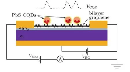
Fig.1.Schematic illustration of the hybrid CQDs/graphene device. Due to the charge transfer between CQDs and graphene,the CQDs are positively charged and give rise to potentialVCQDthat can potentially affect the transport properties of the bilayer graphene underneath.
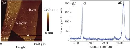
Fig.2.Structure characterization of the bilayer graphene.(a)AFM image of the graphene flakes before the device fabrication.(b)The Raman spectrum measured from the device area of the sample.The measurements were carried out at room temperature with 514-nm laser excitation.
3.Results and discussion
Figure 3(a)shows the resistance R of the hybrid CQDs/graphene device as a function of back gate voltageVBGat T=1.9 K at zero magnetic field and B=4.8 T.After depositing the PbS CQDs,the mobility of the device was found to be similar to before.At B=4.8 T,clear undulation of transfer characteristics is observed,indicating the formation of quantum Hall states at high magnetic fields.Due to the two terminal measurement con figuration employed in this study,R(VBG)is the mixture of contribution from both the longitudinal and the transverse resistance.Quantum Hall regime with filling factor ν=4,8,and 12 is marked in Fig.3(a).In
The fabricated CQDs/graphene devices were measured at low temperatures using a quantum design physical property measurement system(PPMS).Magnetic fields up to 9 T were applied perpendicular to the device plane.All transport measurements were carried out using standard low frequency lockin techniques with a typical bias voltage of 100µV and a 13.3-Hz operating frequency.Before quantum dot deposition,the graphene devices were characterized and the mobility was estimated to be about 8000 cm2·V-1·s-1-9000 cm2·V-1·s-1.comparison to pristine graphene devices,the presence of PbS CQDs increases the sheet resistivity,and demonstrates a localization behavior at low temperatures.Figure 3(b)shows a temperature dependence of the conductance at zero magnetic field and at VBG=-10 V.The conductance decreases as the temperature decreases,indicating a localization effect.The weak localization(WL)correction is clearly visible as a logarithmic temperature dependence of conductance below 30 K.WL arises from interference between time-reversed paths and leads to conductance decrease in the presence of disorder.[22]Time reversal symmetry can be broken by applying a magnetic field,which suppresses weak localization and results in a conductance drop near zero magnetic field,as shown in Fig.4(a).Since the wave functions of graphene are composed of the contributions from two sublattices,the carriers in graphene have chirality.The quantum interference of electrons in monolayer and bilayer graphene is different from conventional 2D systems due to an additional Berry phase.[10-12]On the other hand,intra-valley and inter-valley scattering by defects in graphene are able to scatter electrons and mix the two valleys.[23,24]In our devices,as was discovered earlier,the charge transfer process between the hybrid system leads to positively charged CQDs,which imposes a Coulomb potential on graphene(illustrated as VCQDin Fig.1).[25]The CQDs can also create strain on the graphene underneath,which can also cause the scattering of carriers.[26]Consistent with the above considerations,we have observed that the magnitude of the quantum correction at low temperature is enhanced after depositing the CQDs.It suggests that the coupling between CQD potential and carriers in graphene enhances inter-valley scattering and weak localization effects.
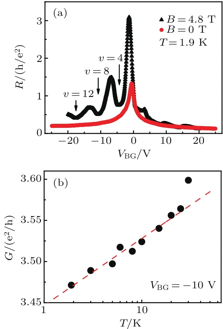
Fig.3.The observation of quantum Hall effect and weak localization for hybrid CQDs/graphene device.(a)The resistance of the PbS quantum dots/graphene device as function of the back gate voltage VBG,taken at B=0 T(red circle)and B=4.8 T(black triangle).The measurements are performed with two probe measurement at low temperature T=1.9 K and at B=4.8 T.The formation of quantum Hall states with different filling factors ν can be clearly seen. ν =4,8,and 12 on the hole side are marked with arrows.(b)The temperature dependence of the conductance at VBG=-10 V and B=0 T.The red dashed line is the linear fitting of the data in the semilogarithmic scale.
The results of the magnetoconductance measurements at a temperature of 1.9 K are performed before and after the deposition of CQDs,which are plotted in Fig.4 labeled as“w/o CQDs”and “with CQDs”,respectively.Both near zero magnetic field and in high field,oscillatory components can be clearly seen,which are periodic with magnetic field.Firstly,we focus on the low magnetic field regime.For the pristine device w/o CQDs,the magnetoconductance increases as a function of magnetic field in the magnetic field range|B|<0.04 T,as shown in Fig.4(c).The positive magnetoconductance results from the effect of WL.The magnetoconductance at low magnetic fields can be fitted to the Hikami-Larkin-Nagaoka equation following Refs.[27]and[28],and the fitted curves are shown with solid red curves in Fig.4(c)and the inset of Fig.4(a)for the results obtained w/o and with the CQDs.The fittings yield the characteristic lengths for phase coherence transport Lφ,which is around 211 nm and 210 nm respectively before and after the deposition of CQDs.These values are comparable with the previously reported phase coherence lengths on bilayer graphene.[27,29,30]In a slightly higher field range 0.04 T<|B|<0.5 T,the universal conductance fluctuations(UCF)dominates and leads to aperiodic undulation of the magnetoconductance.[31]After deposition of CQDs,in addition to the WL and UCF feature,ΔG acquires oscillations with magnetic field.To make the oscillatory behavior apparent and yield better comparison between the results with and w/o CQDs,we have subtracted the low-frequency background(red dashed curve)in both Figs.4(a)and 4(c)from the ΔG(B)data and performed fast Fourier transformation(FFT)on the residual signal.The results are plotted in Fig.4(e).FFT on the results with CQDs shows the primary peak located at 13 T-1with its second harmonic visible.Whereas the peak disappears in the FFT spectrum of the pristine device w/o CQDs.We note that the latter shows a broadened structure that is likely resulting from the residual of the UCF.Since the magnetoconductance oscillation is only observed after the deposition of CQDs,it suggests that the magnetoconductance feature is caused by the CQDs rather than intrinsic behavior of the graphene FETs or residues induced during the FETs fabrication process.The oscillatory magnetoconductance in this regime can be explained by the periodic orbit theory,where periodic orbits lead to a modulation in the density of states.[32]In a periodically perforated two-dimensional electron gas system,quantum mechanical calculation of the magnetoresistance has shown an Aharonov-Bohm(AB)type oscillation that is attributed to the existence of a periodic orbit.[33]In our case,the period of oscillation is ΔB=0.075 T corresponding to the AB oscillation period generated by a periodic potential with a unit cell size of 265 nm.As revealed by earlier results,the solution processed CQDs tend to self-assemble and cluster to 2D arrays on the graphene FETs.[34-37]The discontinuity of the CQD arrays and clustering of the CQDs give rise to a quasi-periodic potential modulation in graphene serving as the source of the observed oscillations.
We now turn to the high magnetic field region.Figure 4(b)shows another oscillation observed for a device with CQDs in the field range of 5 T<B<7.5 T,which corresponds to the quantum Hall transition region between the quantum Hall states with filling factor ν=4 and 8.In Fig.4(d),the magnetoconductance result is also shown for the same device before the deposition of CQDs in the similar magnetic field and gate voltage range and the magnetoconductance oscillation disappears.Following the similar data processing procedure as for the low field results,we have performed FFT on the high- field magnetoconductance data obtained before and after the deposition of CQDs and the results are plotted in Fig.4(f).The Fourier power spectrum of oscillation from the CQD-decorated device reveals a primary peak centered around 3.3 T-1,corresponding to an oscillation period of 0.3 T.The peak is absent from the reference FFT spectrum obtained before the deposition of CQDs,which suggests the important role of the CQD potential.The feature in the spectral range of 1 T-1to 2 T-1,appearing in both curves before and after CQDs are deposited,is an artifact of the windowing function for performing the FFT.The AB-like oscillation in the high magnetic field regime can be understood in terms of the quantum edge state scattering in the integer quantum Hall states.In the quantum Hall regime,the energy spectrum of graphene is quantized,and quantum edge states are formed along the edge of the sample and around the potentials induced by PbS CQDs.This is illustrated in Figs.4(g)and 4(h)for device w/o and with the CQD potential.The localized electronic orbits around a single antidot have been studied in the integer and fractional quantum Hall regime by measuring AB oscillations of conductance to understand the interference and interactionbetween Laughlin quasiparticles.[38,39]Themagnetoconductance is dominated by the scattering behavior between the quantum edge states.In the absence of VCQD,backscattering of the chiral edge state(arrow in Fig.4(g))at the boundary of the graphene device is prohibited.After the CQDs are introduced,one can consider an isolated potential hill in graphene induced by CQDs.In the quantum Hall transition regime,backscattering of the edge state can take place via the resonant transmission by edge channels localized at VCQDwhich are illustrated in Fig.4(h).As we ramp up the magnetic field,the magnetic flux threading the enclosed area(A)of the quantum edge state changes and induces modulation of the tunneling scattering rate and hence the magnetoconductance following the flux quantization condition:
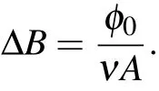
Here,ν is the filling factor,φ0is the magnetic flux quanta,and ΔB is the magnetic field period of the AB-like oscillation.Following the equation,the ΔB=0.3 T thus corresponds to the diameter of the orbits of 132 nm.Such a large lateral scale of the orbit indicates a large size of VCQDwhich is not likely to have been created by isolated CQDs with a size of 5 nm.A more probable picture is that the CQDs cluster and self-assemble to islands of 2D arrays with different degrees of clustering on the graphene surface.The averaged diameter of the dominant localized quantum edge state orbit is around 132 nm as suggested by our results.
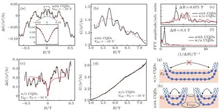
Fig.4.Quantum oscillations induced by graphene-CQDs coupling.Panels(c)and(a)are the magnetoconductance ΔG trace at low magnetic field regime obtain before and after the deposition of CQDs(black solid line).The red dashed line shows the smoothed slow varying background of the ΔG.The inset in panel(a)shows the close-up of ΔG around B=0 T(black symbols),where a signature of weak localization is identi fied and fitted(red solid line).The same fitting is also performed in panel(c)and shown with the red solid line.Panels(d)and(b)are the high field magnetoconductance G(B)before and after the deposition of CQDs.A smoothed background(red dashed line)is shown as a guideline for the oscillatory structures.Panels(e)and(f)are the FFT spectra of the oscillatory components for low field and high field magnetoconductance.Panels(g)and(h)are the schematics for quantum edge state scattering without and with the CQD potential.All the measurements are carried out at 1.9 K.
We note that the sizes of the effective orbit derived from the low field and high results are quite different.The low field magnetoconductance oscillation originates from the modulation of the density of state due to the quasi-periodic potential of VCQD.A similar phenomenon has been observed and investigated in GaAs/AlGaAs two-dimensional electron system with fabricated antidot arrays.[32,40]The diameter estimated from the low field results corresponds to the effective period-icity of VCQD.While the high field magnetoconductance oscillation is due to the AB effect resulting from the localized quantum edge states that enclose the VCQD,it disregards the periodicity of the potential.The clustering of CQDs thus may play more important roles for the high field results.Since in the low field and high field regime,the magnetotransport is sensitive to different aspects of VCQD,and it is expected that the characteristic lengths will be different.Such results also suggest thatVCQDis complicated probably due to different degrees of self-assembling and clustering of CQDs on graphene surface.
4.Conclusion
In summary,we have performed low-temperature magnetotransport measurements on bilayer graphene decorated with PbSCQDs.Thetemperaturedependenceoftheconductanceis logarithmic,as expected for the weak-localization effect in the diffusive regime.The magnetoconductance exhibits oscillations both in the low magnetic field region and in the quantum Hall regime.These oscillations can be related to the scattering potential introduced by CQDs.Our results suggest that the distributed CQDs upon graphene would modify the transport properties of graphene layers and bring out abundant new physics phenomena to be studied in the hybrid graphene systems.
猜你喜欢
内燃机工程(2021年5期)2021-10-19
小学生作文辅导(2021年9期)2021-04-14
江苏教育·书法教育(2021年3期)2021-01-17
中成药(2017年4期)2017-05-17
现代传输(2016年5期)2016-12-19
现代传输(2016年4期)2016-12-01
现代传输(2016年2期)2016-12-01
现代传输(2016年2期)2016-12-01
学生天地·小学低年级版(2014年8期)2014-09-19
学生天地·初中(2014年5期)2014-07-23

- Chinese Physics B的其它文章
- Topological superconductivity in a Bi2Te3/NbSe2heterostructure:A review∗
- The universal characteristic water content of aqueous solutions∗
- Neutral excitation and bulk gap of fractional quantum Hall liquids in disk geometry∗
- Direct deposition of graphene nanowalls on ceramic powders for the fabrication of a ceramic matrix composite∗
- Hard carbons derived from pine nut shells as anode materials for Na-ion batteries∗
- Crystal structures and sign reversal Hall resistivities in iron-based superconductors Lix(C3H10N2)0.32FeSe(0.15<x<0.4)∗