
点缺陷石墨烯的电导
2019-10-14 07:56刘南舒周思赵纪军
物理化学学报 2019年10期
刘南舒,周思,赵纪军
大连理工大学三束材料改性教育部重点实验室,辽宁 大连 116024
1 lntroduction
Owing to the fascinating properties, such as ultra-high carrier mobility, superior electrical and thermal conductivities,graphene is among the most promising materials for future electronics1,2. Extensive efforts have been devoted to fabricate large-scale and high quality graphene sheets, via mechanical exfoliation3, chemical vapor deposition (CVD)4,5, epitaxial growth on metal or SiC substrates6, etc. However, defects are inevitable in the fabricated graphene samples7,8, and they can appreciably affect the material properties8-10, such as opening an energy gap, inducing local charging or magnetic moments,degrading the carrier mobility, and altering the interaction strength between graphene and substrates7,11-14. Understanding the defect impacts is crucially important for device applications of graphene.
Point defects are most commonly observed in synthetic graphene8,9,15,16and their properties have been intensively studied by experiment8,16-19. For instance, zigzag-oriented divacancies and multi-vacancies composed of rotated hexagons are favorably formed by electron irradiation of graphene, and the former exhibits metallic behavior17, while the latter opens a bandgap up to 0.2 eV16. Atomic defects in graphene can lead to sublinear dependence of conductivity on carrier density, distinct from the linear dependency observed for charge impurities20. As the defect concentration increases, an almost insulating behavior was observed for n-type conduction while a metallic behavior was observed for p-type conduction, the conductance showed a plateau above the Dirac point and suppression of ambipolar behavior in graphene21. Lattice defects can also cause significant intervalley scattering, giving rise to constant mobility and insulating temperature dependence of conductivity, both are much lowered than those of graphene with charge impurities22.Moreover, reconstructed vacancies in graphene serve as efficient trapping centers for metal atoms, which can be used for engineering the local electronic and magnetic structure of graphene23.
On the theoretical aspect, point defects were shown to prominently modify the electronic band structure of graphene24-26. They can induce localized states and sharp resonant states at Fermi energy27, which acts as scattering centers for electrons and remarkably reduces the electrical conductivity of graphene28-33. The conductance decreases as the defect concentration increases due to more resonant states in the transport spectrum34,35. However, such a suppression seems to be weakened at the charge neutrality point, leading to a minimum conductivity of 4e2/πh even for higher defect concentrations36. Single vacancies behave as hole dopants24,while Stone-Waals defect and double vacancies can open band gap up to 0.3 eV in graphene37,38.
Despite of the aforementioned successes, the role of point defects on the electrical transport properties of graphene is not entirely understood. Some critical issues remain to be solved.For instance, how is the electron conduction in graphene affected by various types and concentrations of point defects? How is the electrical transport property of defective graphene correlated to the band structure? To address these questions, here we systematically explored the electrical transport properties of graphene with various point defects by density functional theory(DFT) calculations combined with the non-equilibrium Green’s function (NEGF) method. We find striking difference in the electrical conductance of graphene with various types of point defects, which can be correlated to the energy splitting at the Dirac point. Our theoretical results provide vital insights into the electrical transport properties of realistic graphene sheets, and would be helpful for experimental synthesis of graphene-based electronics of high performance.
2 Computational method
The electron transmission in graphene monolayer with point defects was simulated by DFT within the Keldysh nonequilibrium Green’s function framework implemented in the QuantumWise Atomistix Toolkit (ATK) package39-41, using a cutoff energy of 2040 eV and the generalized gradient approximation parameterized by Perdew, Burke and Ernzerhof(GGA-PBE) for the exchange-correlation functional42. The wave functions were expanded by a numerical basis set of double-ζ plus polarization (DZP). As displayed by Fig. 1, we adopted a two-probe model composed of three parts: the left and right electrodes made of semi-infinite graphene, the scattering region comprising defective graphene monolayer, and the buffer regions as continuation of the graphene electrodes. Charge carriers transport along the zigzag direction of graphene (Γ to X in the first Brillouin zone in Fig. 2a). The scattering region consist of 10 × n (n = 5, 6, 7, 8) graphene unit cells incorporated with point defects, corresponding to lateral dimensions of 2.46 nm and 2.56-3.44 nm along and perpendicular to the transport direction, respectively. The electrode and buffer region include 2 × n (n = 5, 6, 7, 8) graphene unit cells. Periodic boundary condition was adopted perpendicular to the transport direction.A vacuum region of 2 nm was added to the out-of-plane direction to avoid the interactions between the neighboring layers. The Brillouin zone was sampled by a Monkhorst-Pack 50 × 5 × 1 kpoint mesh. With such a k-point sampling, the Dirac cone of graphene lead can be clearly seen in the band structure (Fig. S1,Supporting Information). The defective graphene monolayer(scattering region) was optimized for the ionic and electronic degrees of freedom using the criteria for total energy of 10-4eV and force on each atom of 0.2 eV·nm-1, using an orthorhombic supercell periodic for both two lateral directions, as shown in Fig. 2. The electronic band structure of the scattering region was calculated, using a convergence criterion of 10-6eV for total energy, which achieved convergence according to our test (see Fig. S2, Supporting Information).

Fig. 1 Two-probe model of graphene monolayer with point defects for simulating the electrical transport properties.The transport direction is along the x axis. Periodic boundary condition is applied to the y axis.
We tested scattering regions with larger transport lengths up to ~3 nm. The computed transmission spectrum T(E) remains the same for transport length above ~2.4 nm, suggesting that ballistic transport regime is achieved at this length scale.Therefore, the electrical conductance can be calculated from T(E) based on the Landauer-Buttiker formalism under the linear response approximation43:

where e is electron charge, h is Planck’s constant, f0is the Fermi-Dirac distribution function:

with the electron temperature T = 300 K (kBis Boltzmann constant and EFis the Fermi energy).
3 Results and discussion
As shown by Fig. 2, we consider a total of seven kinds of point defects incorporated in graphene monolayer, including Stone-Waals defect (SW), inverse Stone-Waals defect (inverse-SW),single vacancy (SV), SV undergone a Jahn-Teller distortion(SV5-9), and double vacancies composed of different defect rings (DV585, DV555777 and DV5555-6-7777, see Fig. S3 of Supporting Information). These point defects are most commonly observed in synthetic graphene samples8. The concentration of point defects (c) is defined as the number of point defects in the scattering region divided by the width (w) of the scattering region perpendicular to the transport direction. The considered defect concentration in this work is 0.29-0.78 nm-1,falling in the range of the experimental values (0.10-0.59 nm-1)21.We also examined graphene with even lower defect concentration c = 0.23 nm-1, which gives very similar transmission spectra as that of c = 0.29 nm-1(see Fig. S4,Supporting Information). For all the considered systems, the defective graphene sheets have a planar structure without any noticeable buckling. The energetic stability of defective graphene is characterized by the formation energy ΔH:
ΔH = (Edefect- N × μC)/n (3)
where Edefectis the energy of defective graphene consisting of N number of C atoms; μCis the energy of a C atom in perfect graphene; n is the number of point defects in the scattering region. Point defect with larger positive ΔH value is less energetically stable and more difficult to form in synthetic graphene. As revealed by Table 1, the graphene point defects have formation energies of 4.02-7.88 eV. Generally, the formation energies of various defects follow the sequence:Stone-Waals defects < double vacancies < single vacancies.Stone-Waals defect is most stable in our considered point defects, which is consistent with the previous report8. For each type of point defect, the formation energy increases with the increase of defect concentration.
Fig. 3 shows the transmission spectra at zero bias voltage of defective graphene monolayers. Obviously, the presence of point defects is detrimental to the electron transport in graphene.Compared to double vacancies, Stone-Waals and single vacancy defects have relatively small impact on the transmission spectrum. In particular, at low concentrations (c = 0.29-0.39 nm-1), the transmission coefficients of SW and inverse SV defects are almost identical to that of graphene in the vicinity of Fermi energy (electron energies of -0.5 - 0.3 eV). Beyond this energy range, the transmission spectra of Stone-Waals and single vacancy defects are moderately reduced with respect to perfect graphene. Some dips are present in the transmission spectra,which are attributed to the localized states induced by the defects and would lead to the suppression of transmission channels44.High concentrations of defects (c ≥ 0.58 nm-1) severely destruct the electron transport in graphene, with transmission coefficientsreduced by 3-5 times with regard to perfect graphene. For all these point defects, the transmission spectra reveal distinct asymmetric electron and hole conduction.

Table 1 Formation energy (ΔH), energy splitting at the Dirac point(Δ) and ratio between average electrical conductance of graphene monolayer with point defect (Ge) and that of pristine graphene(Ge0) (between ±0.5 eV) at various concentrations (c).
To quantitatively evaluate the electrical transport properties of the defective graphene monolayers, we calculated the ratio between the average electrical conductance (Ge·G-1e0), which is

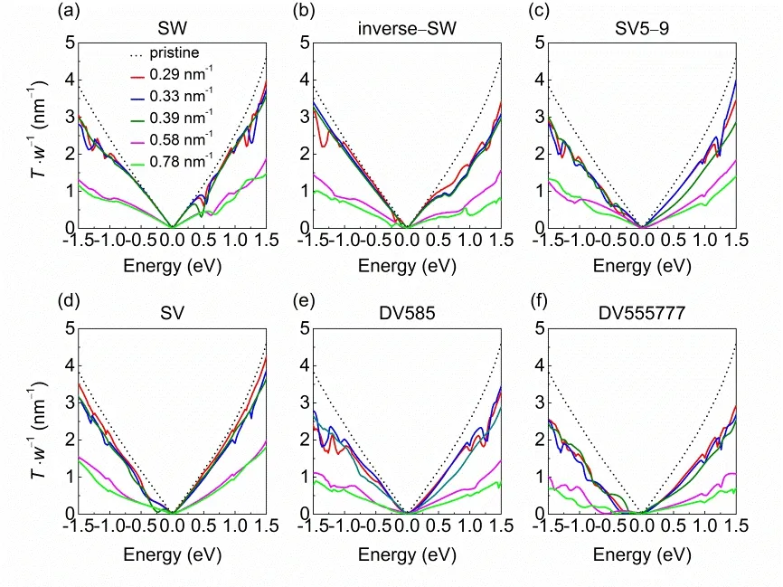
Fig. 3 Transmission spectra per unit width (T·w-1) for graphene monolayer with (a) SW, (b) inverse-SW, (c) SV5-9, (d) SV,(e) DV585 and (f) DV555777 defects at various defect concentrations (colored solid lines).The transmission spectrum of perfect graphene is shown by black dashed line. The Fermi energy is shifted to zero.

Fig. 4 Ratio between average electrical conductance of graphene monolayer with point defect (Ge) and that of pristine graphene (Ge0) (between±0.5 eV) as a function of (a) defect concentration (c) and (b) energy splitting at the Dirac point (Δ) for graphene monolayer with various point defects.The dashed lines are the fit of Ge·G-1 e0 vs c and Ge·G-1 e0 vs Δ with exponential functions.
where G(E) and G0(E) are the electrical conductance with and without defects, respectively. Ge·G-1e0(between ±0.5 eV) as a function of defect concentration and energy splitting at Dirac point are plotted in Fig. 4. Ge·G-1e0of various point defects follows the sequence: SW > inverse-SW > SV5-9 > SV >DV585 > DV5555-6-7777 > DV555777. At low concentrations,SW, inverse-SW and SV5-9 almost retain the electrical conductance of perfect graphene, SV and DV585 defects induce moderate reduction of 25%-34%, and DV55577 and DV5555-6-7777 show largely suppress by 51%-62% of that of graphene.As the defect concentration increases to above 0.58 nm-1,Ge·G-1e0shows the reduction of average electrical conductance by a factor of 2-3 compared to the values of graphene monolayers with low concentration of point defects.
To gain further insights into the electrical transport properties of various point defects, we examine the band structures of the scattering region along the transport direction (zigzag direction).As illustrated in Fig. 2, charge carriers transport along the x axis,corresponding to the direction from Γ to X point in the first Brillouin zone. The band structures and local density of states(LDOS) are presented in Fig. 5. The conical point of perfect graphene monolayer with a rectangular supercell along the zigzag direction is identified as the Dirac point (K point in the Brillouin zone as indicated in Fig. 2a). All the point defect systems show some flat bands close to Fermi energy, which are dominated by the C atoms in the defect region (see the partial charge densities in Fig. 5), and result in resonant peaks close to Fermi energy in the local density of states (LDOS). Due to the breaking of intrinsic symmetry of the graphene honeycomb lattice, the band degeneracy at the Dirac point is removed, giving rise to an energy splitting45,46, which is the energy difference between the two bands near Fermi energy at K point.Considering defect concentration of c = 0.39 nm-1as representative, graphene with SW defect induces a defective π state at about 0.5 eV above Fermi energy. It maintains the linear dispersion with the conical point slightly shifted from the Dirac point, giving an energy splitting of 0.05 eV. For inverse-SW,SV5-9 and SV defects, the induced localized states are closer to Fermi energy and narrow gap of 0.06-0.10 eV is opened near the Dirac point. In presence of double vacancies, the band structure of graphene is severely disturbed—the valence band maximum(VBM) and conduction band minimum (CBM) are shifted to the Γ or Z point giving small indirect gap of 0.04-0.10 eV, which may help improve the on/off ratio of graphene-based field effect transistor21. The Dirac point of DV555777 shifts up by about 0.25 eV relative Fermi energy, leading to Δ = 0.33 eV. The density of states of double vacancies shows more localized states around the defective C atoms, which may result in stronger scattering of carriers and thus more suppressed transmission spectrum. Accordingly, the partial charge densities reveal enhanced localization in the defect region for double vacancies,such that the charge carriers are hindered by these states, leading to the reduction of electrical conductivity of the graphene sheet.
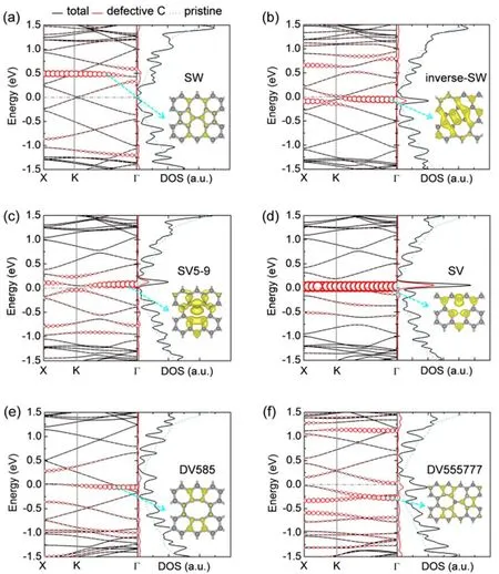
Fig. 5 Band structures (left panels) and density of states (DOS)(right panels) of graphene monolayer with various point defects:(a) SW, (b) inverse-SW, (c) SV5-9, (d) SV, (e) DV585 and (f) DV555777,at defect concentration of 0.39 nm-1.In the left panels, the red circles show the bands from C atoms in the defect region,and the radius of the circles is proportional to the weight. In the right panels,the black solid line shows the total DOS of defective graphene monolayers,the red solid lines show the DOS from C atoms in the defect region, and the light blue dashed line shows the DOS of perfect graphene. The insets display the partial charge densities of the localized states indicated by the cyan dashed arrows, with an isosurface value of 1.5 e·nm-1. The Fermi energy is shifted to zero.
Interestingly, the electrical conductance at Fermi energy of the defective graphene monolayers is correlated to their energy splitting at the Dirac point in the band structures. As demonstrated by Fig. 4b, Ge·G-1e0decreases exponentially as Δ increases. Compared to Stone-Waals and single vacancy defects(Δ = 0.03-0.09 eV), double vacancies have large Δ (0.18-0.33 eV) and thus induce prominent reduction of electrical conductance. As defect concentration increases, the energy splitting rises 2-3 times of the values of graphene with low concentrations of point defects.

Fig. 6 Band structure (left panels) and density of states (DOS)(right panels) of graphene monolayer with SW defect at various concentrations: (a) 0.29 nm-1, (b) 0.39 nm-1, (c) 0.58 nm-1 and (d) 0.78 nm-1.In the left panels, the red circles show the bands from atomic orbitals of C atoms in the defect region, and the radius of the circles is proportional to the weight. In the right panels, the black solid line shows the total DOS of defective graphene monolayers,the red solid lines show the DOS from C atoms in the defect region, and the light blue dashed line shows the DOS of perfect graphene. The insets display the partial charge densities of the localized states indicated by the cyan dashed arrows, with an isosurface value of 1.5 e·nm-1. The Fermi energy is shifted to zero.
Fig. 6 shows the band structures and LDOS of graphene monolayer with various concentrations of SW defect (see Figs.S5-S10 of Supporting Information for the other point defects).The energy splitting (Δ) and the energy of the band bottom to the Fermi energy (Ebottom) as a function of defect concentration is depicted in Fig. S11 (Supporting Information). Δ and Ebottomfollow the opposite sequence of Ge·G-1e0: SW < inverse-SW <SV5-9 < SV < DV585 < DV5555-6-7777 < DV555777. For c ≤0.39 nm-1, Δ and Ebottomare linear dependence to c, which is consistent to literature46. As defect concentration increases,more flat bands are present near Fermi energy, and density of states shows more localized states on C atoms in the defective region, which may enhance the scattering of electrons34,according induce more conduction dips at the Fermi energy in the transmission spectrum. The corresponding partial charge densities exhibit enhanced localization with higher defect concentration. Consequently, charge carriers are hindered by these localized states and electron conduction is severely destructed in graphene with high concentrations of point defects.
4 Conclusions
In summary, the electrical transport properties of graphene monolayer carrying various point defects were systematically explored by density functional theory calculations with the nonequilibrium Green’s function method. The point defects induce localized states near Fermi energy and give rise to energy splitting at the Dirac point due to the breaking of intrinsic symmetry of the graphene honeycomb lattice. The electrical conductance shows exponential decay as the energy splitting increases, and it highly depends on the type and concentration of point defects in graphene. Low concentrations of Stone-Waals defect do not noticeably degrade the electron transport in graphene, while double vacancies severely reduce the electrical conductance of graphene by a factor of 2-3. These theoretical results elucidate the impact of various structural defects on the electrical transport properties of graphene monolayer, and reveal the key parameters for modulating the electrical conductance of defective graphene.
Supporting lnformation:available free of charge via the internet at http://.
猜你喜欢
湖北大学学报(自然科学版)(2022年5期)2022-09-07
健康护理(2022年3期)2022-05-26
建材发展导向(2021年15期)2021-11-05
食品安全导刊(2021年21期)2021-08-30
大学(2021年2期)2021-06-11
能源工程(2021年1期)2021-04-13
小学生优秀作文(低年级)(2020年6期)2020-07-06
中文信息(2020年3期)2020-04-14
大东方(2019年1期)2019-09-10
校园英语·上旬(2019年2期)2019-04-08
