
Transport properties of Tl2Ba2CaCu2O8 microbridges on a low-angle step substrate
2021-06-26 03:03ShengHuiZhao赵生辉WangHaoTian田王昊XueLianLiang梁雪连ZeHe何泽PeiWang王培LuJi季鲁MingHe何明andHuaBingWang王华兵
Chinese Physics B 2021年6期
关键词:生辉
Sheng-Hui Zhao(赵生辉) Wang-Hao Tian(田王昊) Xue-Lian Liang(梁雪连) Ze He(何泽)Pei Wang(王培) Lu Ji(季鲁) Ming He(何明) and Hua-Bing Wang(王华兵)
1College of Electronic Information and Optical Engineering,Nankai University,Tianjin 300350,China
2Research Institute of Superconductor Electronics,Nanjing University,Nanjing 210093,China
3Beijing Institute of Radio Measurement,Beijing 100854,China
4Key Laboratory of Photoelectronic Thin Film Devices and Technology of Tianjin,Tianjin 300350,China
Keywords: high temperature superconductors,Tl-2212,intrinsic Josephson effects,transport properties
1. Introduction
The high transition temperature (high-Tc) cuprate superconductors, most of which are anisotropic compounds, have layered crystal structures to form natural superconducting-blocking-superconducting trilayer sandwich structures repeatedly.[1,2]Their layered crystal structure leads to the current transport via tunneling, which is dominated by intrinsic Josephson effect (IJE). Kleiner and co-workers[3]showed the intrinsic Josephson effects in Bi2Sr2CaCu2O8(BSCCO), (PbyBi1−y)2Sr2CaCu2O8(PBSCCO),and Tl2Ba2Ca2Cu3O8(Tl-2223)compounds. TheI–Vcharacteristics of intrinsic Josephson junction(IJJ)exhibited both clear hysteresis and multiple branches,indicating a series connection of highly capacitive junctions. BSCCO intrinsic Josephson junctions have been extensively studied[4–6]as terahertz (THz) emitters.[7–14]In BSCCO IJJ stacks, superconducting CuO2planes alternating with insulating SrO and BiO layers can realize verticalc-axis transport.This natural layered structure can be applied to generate electromagnetic radiation in the terahertz regime. Additionally, it is very convenient to fabricate IJJs by growing Tl-based films on a vicinal cut substrate. Tl-2212 has an operating temperature over 100 K,[15]which is much higher than that of BSCCO and YBa2Cu3O7−δ(YBCO). Intrinsic Josephson effects and other superconducting properties of Tl-2212 IJJs were mostly investigated on misaligned substrate,[16–28]in which films were grown epitaxially on the substrate with the same misalignment angle. In this structure,the copper oxide planes of Tl-based films create a misaligned angle with respect to the substrate surface, the superconducting current can then flow through the inter-plane along thec-axis of the sample films according to the experimental design.
Alternatively, to exploitc-axis transport, superconducting films can be deposited on a substrate into which a step has been etched. Wanget al. successfully fabricated IJJs in oxygen-deficient YBCO films on a low-angle SrTiO3step substrate.[29,30]Several studies[31,32]indicated that Tl-based superconducting microbridges fabricated on substrates with high step angles(usually 60◦–75◦)exhibited intrinsic Josephson effects,whereas microbridges on substrates with step angles lower than this interval did not show intrinsic Josephson effects due to the flux-flow effects. Some experts have different opinions on this conclusion. Yoshikawaet al. reported that both types of step-edge junctions or IJJs can be shown on a step substrate of the same angle(about 28◦),which depends on the height of the steps.[33,34]The relationship between the step angle and the type of junctions needs to be verified by further experiments. More studies are essential to provide evidence for this field.
In this work, we use conventional photolithography, together with focused ion beam (FIB) direct-write lithography to fabricate superconducting microbridges on LAO step substrates. With our improved two-step method,[35,36]we present fabrication and electrical transport characterization of intrinsic Josephson junctions in Tl-2212 superconducting microbridges on a step substrate. We investigate the current–voltage characteristics of superconducting microbridges at different temperatures. We also discuss the features of IJEs,i.e.,hysteresis structures and voltage jumps,in current-biased Tl-2212 microbridges.
2. Experimental method
At first, LAO substrate was etched with Ar-ion milling through a photolithography defined mask. The modified substrate has a very smooth step with the angle of∼30◦measured with an atomic force microscopy(AFM).Tl-2212 films were then deposited on LAO step substrates by an improved two-step method,including dc magnetron sputtering and post annealing. This method can maintain the vapor-solid equilibrium during the formation of Tl-2212 phase crystals without adding any additional Tl sources and the uniformity of Tl-2212 films was greatly improved.[35]Besides, x-ray diffraction(XRD)was used for observing Tl-2212 phase in the film,and the scanning electron microscope (SEM) image of the Tl-2212 film is shown in Fig. 1(a). After that, microbridges were defined using standard photolithography, and pattern transfer to the Tl-2212 thin films was achieved by Ar+beam etching. Three microbridges with different widths, 4 µm(named sample N1,Tc0=102 K), 6 µm (named sample N2,Tc0=105 K), and 10 µm (named sample N3,Tc0=105 K),were fabricated on the same sample film. Figure 1(b)provides a SEM diagram of a sample microbridge.Au wires were glued onto the electrode contact with silver conductive adhesive for better electrical contact, and transport measurements were performed with a four-point method, as shown in Fig. 1(c).DC current source was used for biasing the samples and the voltage across the bridge was measured via a low-noise amplifier. Figure 1(d)illustrates the schematic of the film growth on a step substrate,black solid line indicates the current direction when applied a biased current in the film.

Fig. 1. (a) SEM image of the film on step substrate, black solid lines are guides for the eyes indicating the step on the substrate. (b) Falsecolor SEM image of a typical 4-µm-wide microbridge. (c) Schematic of four-point measurement setup.(d)Schematic diagram of step growth of intrinsic Josephson junctions.
3. Results and discussion
We firstly investigated the transport properties of samples N1, N2, and N3. TheI–Vcharacteristics of sample N1 measured at 50 K are presented in Fig.2(a). By ramping the bias current up and down, some voltage jumps appear on theI–Vcurve. Besides,several junctions switch from resistance state to zero voltage state along the hysteretic path when decreasing the bias current. These characteristics are typical features of IJEs for serial arrays of intrinsic Josephson junctions.
To further obtain a clear insight into the intrinsic Josephson effects,theI–Vcurves of sample N1 were measured with microwave irradiation. Figure 2(b)shows theI–Vcurves under microwave irradiation (27.1 GHz) at temperatures 50 K and 80 K.As can be seen,the current upturns appear when the microwave power is strong enough. Besides, the microwave frequency 27.1 GHz is much lower than the plasma frequency of Tl-2212 IJJs(about in THz band),which is hardly obtained in the experiments. Therefore, the phase lock between junctions is unstable in our experiment and the microwave induced steps have not been observed.[29]It should be mentioned that the current upturns in Fig. 2(b) are typical characteristics of intrinsic Josephson junctions, which are similar to the results in YBCO film[29]and BSCCO single crystal.[37,38]
To have a better understanding on the effect of microbridge width on the IJEs, we performed a number of additional characterization experiments.Figure 2(c)shows theI–Vcurves of the sample N2 at different temperatures from 45 K to 95 K. Figure 2(d) presents theI–Vcharacteristics of N2 at 45 K. Compared with theI–Vcurves of N1, there are few voltage jumps,and the amplitude of the hysteresis is small on theI–Vcurves of N2. We attribute this phenomenon to the shunted resistance,induced by the defects in the microbridge,partially bypassing the current. As the bath temperature further increases,the voltage jumps and hysteresis structures apparently fade away.
Figure 3 shows a typicalI–Vcurve of sample N3 measured at different temperature. As can be seen, hysteresis structures do not appear,but several voltage jumps can be seen on theI–Vcurves of sample N3 at 5 K in Fig. 3. Additionally, we see a large voltage jump (about 70 mV) on theI–Vcurves, which may be caused by the appearance of hotspot overheating in such high bias current. As shown in the inset of Figure 3, critical currentIcof sample N3 is much higher than that of samples N1 and N2 at the same bath temperature.By considering characteristics of polycrystalline thin film, it can be naturally considered that this may result from the existence of a large number of non-c-axis crystal grains. Because the Tl-based film cannot be prepared by anin-situmethod,the crystallization of the films in the post annealing process is accomplished in a dynamic balance of Tl2O vapor pressure. Inevitably, comparing with YBCO and BSCCO,Tl-based films have much more defects. Therefore,as the width of the microbridge increases,these defects shorten the IJJ junctions along thec-axis direction of Tl-2212 films, resulting in a largeIcvalues in sample N3. And theI–Vcurves of sample N3 are similar to those of normal superconducting microbridges,and do not feature any IJEs at the same bath temperature range(40–90 K).
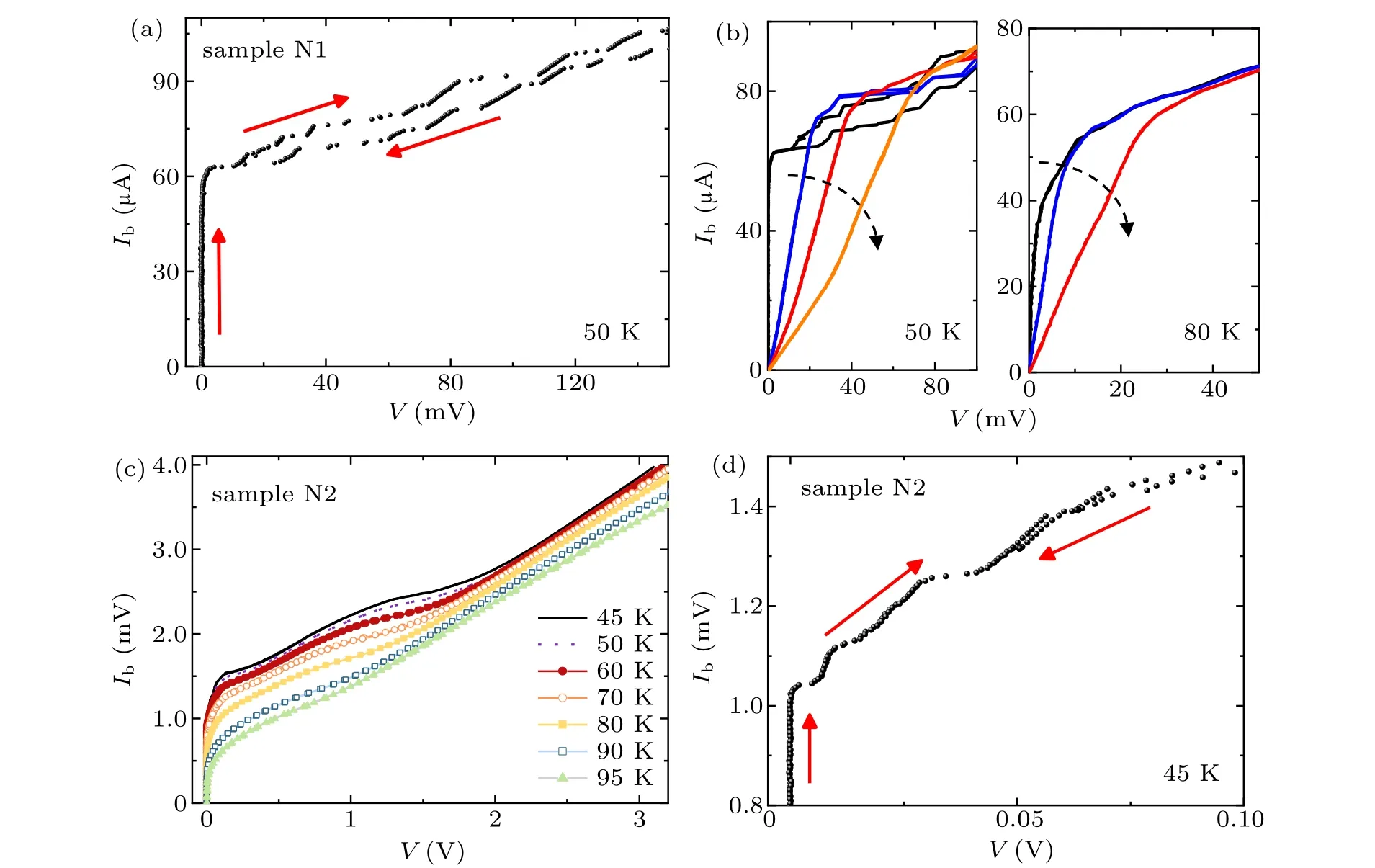
Fig.2.(a)Current–voltage curves for sample N1 measured at temperature of 50 K.(b)The I–V curves of sample N1 under 27.1 GHz microwave irradiation at 50 K and 80 K;the dashed arrows indicate microwave power become lager.(c)The I–V curves of sample N2 measured at different temperatures from 45 K to 95 K.(d)Voltage jumps and small hysteresis measured at 45 K.Solid arrows in(a)and(d)indicate the sweeping direction of the current.
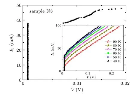
Fig.3.Current–voltage characteristics of sample N3 at 5 K,inset shows a series of I–V curves of sample N3 measured from 40 K to 90 K in steps of 10 K.
From the data discussed above,the characteristics of IJJs in thec-direction of Tl-2212 films are possibly concealed with the increment of defect-induced lattice mismatch. Based on this point of view, as the width of the bridge becomes wider,the critical current becomes larger. Besides, the results of sample N1 show hysteresis structures and voltage branches on theI–Vcurves, which are the typical characters of intrinsic Josephson effects. Whereas no hysteresis structures but only a few voltage jumps are observed in sample N3, indicating that enlarging the width of the microbridges may weaken the characteristics of IJJs. On the contrary, narrow width of the microbridges is favorable to the formation of IJJs,which will be discussed in the following.
Figure 4(a)shows the measuredI–Vcurves of sample S1 at different bath temperatures. In Fig. 4(b), theI–Vcharacteristics demonstrate clear multiple branches with a significant hysteresis by ramping the bias current up and down repeatedly,suggesting that our IJJs made of Tl-2212 thin films on step substrate exhibit clearc-axis transport properties. As shown in Fig. 4(b), when the bias current is ramped from zero, IJJs are initially in their zero-voltage state. When the current is increased to about 12.5 µA, the critical current of the weakest junction is reached and this junction switches to its resistance state. Upon further increase of the bias current,more voltage jumps appear on theI–Vcurves. While the junctions switch from the resistance states to the zero-voltage states individually at different return currents when the bias current is decreased. In this way, multiple branches can be traced out on theI–Vcurves. Normal resistances(Rn)are constant from 5 K to 30 K and have a sharp change when the bath temperature rises up to 40 K, corresponding to the large voltage jumps.It should be noticed thatRnof sample S1 measured at 40 K is larger than that at other temperatures. We believe that this may be caused by a series of IJJs switching to the resistive state directly from the superconducting state.
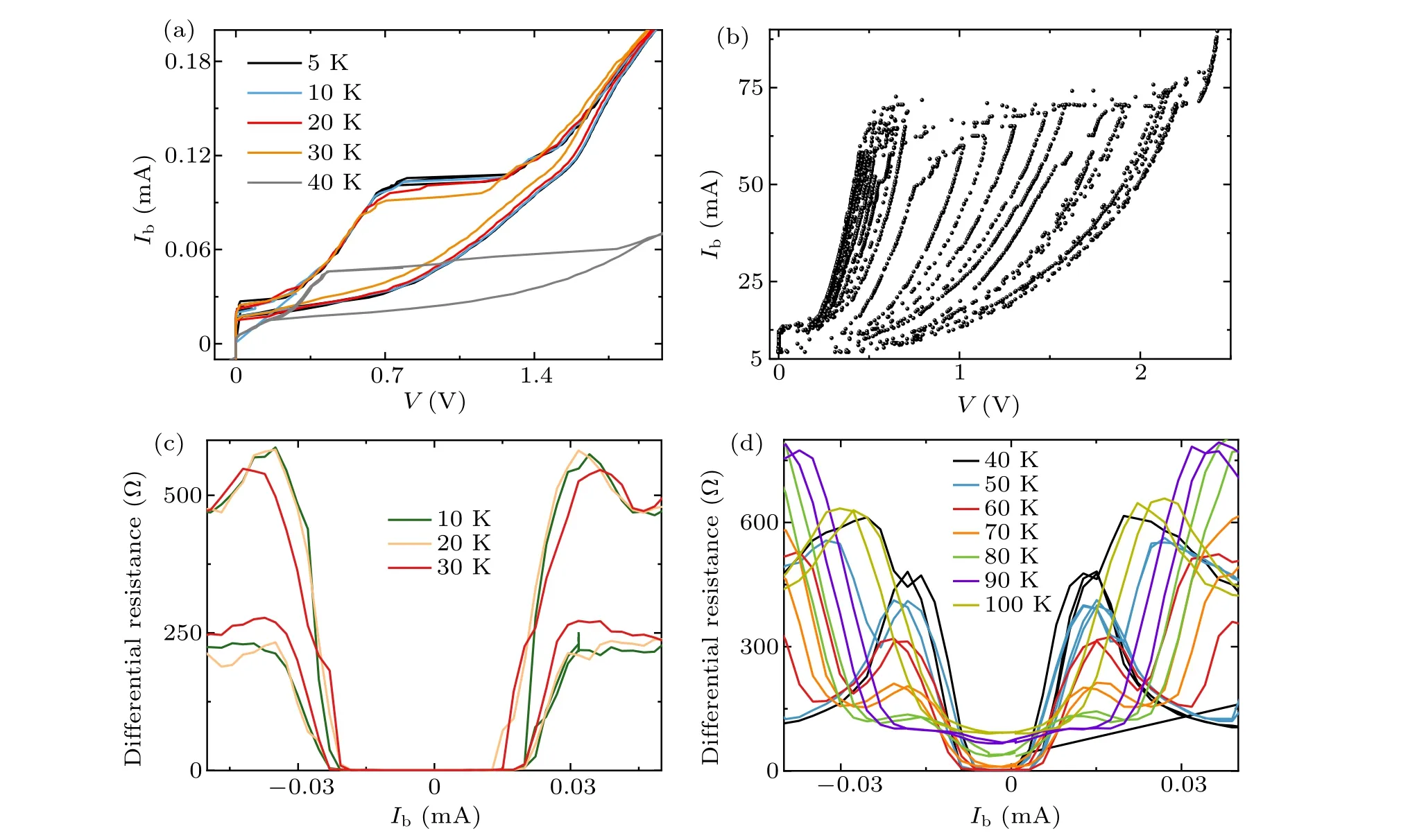
Fig.4. (a)Back-and-forth I–V curves of sample S1 measured at 5 K and 10 K to 40 K with an increment of 10 K.(b)The voltage jumps and hysteresis in I–V curves measured at 5 K.(c)Differential resistance dV/dI versus the bias current Ib for temperatures 10 K,20 K,and 30 K.(d)Differential resistance dV/dI versus Ib for temperatures from 40 K to 100 K in 10 K increments.
Furthermore, we measured the differential resistance using low-frequency techniques. Figures 4(c) and 4(d) plot the detailed variation of the differential resistance (dV/dI) versus bias currentIb, while sweeping bias currentIbfrom negative to positive current. Differential resistance peaks persist in a wide temperature range from 5 K up to 100 K. Unlike the tunnel junctions made from conventional superconductors,the decreasing of differential resistance after the first peak is a common occurrence in HTS tunnel junctions.[39]The superconducting energy gap is not available due to the unknown numbers of IJJs at different bath temperatures. It should be mentioned that,at bath temperature above 60 K,the junctions exhibit some finite resistance. And this finite resistance increases as the bath temperature increases,as plotted in Fig. 4(d). While its exact origin is not clear at this stage, we surmise that the resistance may be caused by a lack of coherent Josephson transport in a series of IJJs. These results together with theI–Vcurves suggest that the IJJs are formed in Tl-2212 microbridge.
In terms of relationship between the microbridge width and IJEs, we observe more obvious IJEs characteristics in a smaller width of bridge.From the result,the narrower width of the microbridge seems to have enhanced the intrinsic Josephson effects. The width scale of the superconducting bridge in the range of nanometers will be studied in the future with the help of FIB.And the measurement of such a nanobridge will be of great interest.
4. Conclusion
To conclude, using an improved two-step method we present the realization of a series of Tl-2212 intrinsic Josephson junctions on a step substrate. By varying the width of the microbridge, we observe the intrinsic Josephson effect in the narrow bridge,and it fades away as the bridge becomes wider.We attribute this to the current bypassing of IJJs and flowing through lattice-induced defects of the film. Our results indicate that the width of the microbridge is crucial to obtaincaxis intrinsic Josephson junctions. Besides, the dependence of step angle and height on Josephson junction type deserves future research.
猜你喜欢
汽车实用技术(2022年12期)2022-07-05
艺术评论(2020年6期)2021-01-22
东坡赤壁诗词(2020年2期)2020-06-04
少儿美术(2019年4期)2019-12-14
云南教育·中学教师(2019年6期)2019-08-13
东坡赤壁诗词(2019年1期)2019-04-30
下一代英才(酷炫少年)(2018年12期)2018-12-29
时代邮刊(2018年18期)2018-11-13
宝藏(2018年8期)2018-08-31
艺术品鉴证.中国艺术金融(2018年12期)2018-08-26

- Chinese Physics B的其它文章
- Quantum computation and simulation with vibrational modes of trapped ions
- ℋ∞state estimation for Markov jump neural networks with transition probabilities subject to the persistent dwell-time switching rule∗
- Effect of symmetrical frequency chirp on pair production∗
- Entanglement properties of GHZ and W superposition state and its decayed states∗
- Lie transformation on shortcut to adiabaticity in parametric driving quantum systems∗
- Controlled quantum teleportation of an unknown single-qutrit state in noisy channels with memory∗