
Terahertz generation and detection of LT-GaAs thin film photoconductive antennas excited by lasers of different wavelengths
2022-02-24 08:59XinLiu刘欣QingHaoMeng孟庆昊JingDing丁晶ZhiChenBai白志晨JiaHuiWang王佳慧CongZhang张聪BoSu苏波andCunLinZhang张存林
Chinese Physics B 2022年2期
关键词:刘欣
Xin Liu(刘欣), Qing-Hao Meng(孟庆昊), Jing Ding(丁晶), Zhi-Chen Bai(白志晨),Jia-Hui Wang(王佳慧), Cong Zhang(张聪), Bo Su(苏波), and Cun-Lin Zhang(张存林)
Beijing Advanced Innovation Center for Imaging Theory and Technology,Beijing Key Laboratory for Terahertz Spectroscopy and Imaging;Key Laboratory of Terahertz Optoelectronics,Ministry of Education,Department of Physics,Capital Normal University,Beijing 100048,China
A new method of generating and detecting terahertz waves is proposed. Low-temperature-grown gallium arsenide(LT-GaAs)thin films are prepared by etching a sacrificial layer(AlAs)in a four-layer epitaxial structure constituted with LT-GaAs,AlAs,GaAs,and semi-insulating gallium arsenide(SI-GaAs). The thin films are then transferred to clean silicon for fabricating the LT-GaAs thin film antennas. The quality and transmission characteristics of the films are analyzed by an 800-nm asynchronous ultrafast time domain spectroscopy system,and the degree of bonding between the film and silicon wafer is determined. Two LT-GaAs thin film antennas for generating and detecting the terahertz waves are tested with a 1550-nm femtosecond laser. The terahertz signal is successfully detected, proving the feasibility of this home-made LTGaAs photoconductive antennas. This work lays a foundation for studying the mechanism of terahertz wave generation in GaAs photoconductive antennas below the semiconductor band gap.
Keywords: terahertz,low-temperature-grown GaAs,photoconductive antenna,1550-nm laser
1. Introduction
Terahertz (THz) waves are electromagnetic waves in a frequency range of 0.1 THz–10 THz and a wavelength range of 3 mm–0.03 mm,falling between microwave and infrared light.In recent years, the rapid development of ultrafast laser technology and semiconductor material technology has provided reliable, stable excitation light sources for generating the terahertz waves,[1–4]thereby facilitating the advances in generation technology, detection technology, and application technology for terahertz waves and promoting the wide application of terahertz waves in imaging, safety detection, biomedicine,astronomy,and spectroscopy as well.[5–7]
At present, there are two primary methods of generating the pulsed terahertz radiation: photoconductive antennas[8]and optical rectification.[9]With the former method, a femtosecond laser pulse triggers a photoconductor under a DC bias, and a coherent current drives a dipole antenna to generate the terahertz radiation. The latter method, optical rectification, acts via a type of nonlinear effect. Here, a femtosecond laser pulse interacts with nonlinear media(LiNbO3,LiTaO3, ZnTe,etc.) to produce a low-frequency polarization field and then radiates terahertz waves. Wanget al.reviewed the methods of producing terahertz vortex beams,which has a wide application prospect in many fields.[10]Xieet al.[11]proposed a new nondestructive method of testing the cross-linked polyethylene (XLPE) based on terahertz time domain spectrum, which provides a novel concept for the nondestructive testing of cable insulation defects that can also be used to assess other electrical equipment. With the continuous development of semiconductors, the terahertz wave generation using semiconductor materials has become a commonly employed method. Salemet al.[12]and Xuet al.[13]used the ultrashort laser pulses with a femtosecond pulse width to pump optoelectronic semiconductor materials, such as semi-insulating gallium arsenide(SI-GaAs)and low-temperature-grown gallium arsenide (LT-GaAs), to instantaneously excite carriers on the surface of semiconductor material and then radiate terahertz waves.[14]Hattoriet al.[15]studied the time characteristics of terahertz waves generated by a large-aperture photoconductive antenna and considered the influence of semiconductor carrier lifetime and relaxation time on terahertz radiation. The active materials have advantages over traditional terahertz hypersurfaces in dynamic tunable control of terahertz waves.Therefore,some researchers have used this material to generate the terahertz waves.[16]
When an LT-GaAs photoconductive antenna is used to generate the terahertz waves, an 800-nm femtosecond pulse laser is usually used for excitation. In contrast to previous research,the LT-GaAs thin films are prepared by etching sacrificial layer on a four-layer substrate in this study. An LT-GaAs thin film photoconductive antenna is fabricated by bonding and evaporation. In an asynchronous ultrafast time domain spectroscopy system, the quality of the film and the extent of bonding between the film and silicon wafer are measured by an 800-nm femtosecond laser. Subsequently, two home-made LT-GaAs thin film antennas are separated by a distance of 2 mm. The terahertz signal is successfully detected by a 1550-nm femtosecond laser. The structure of the thin film antenna is simpler than that of the epitaxial wafer antenna;moreover,the thin film antenna can reduce the echo and information loss and improve the signal-to-noise ratio.
2. Fabrication and detection of LT-GaAs thin film photoconductive antennas
In this paper,the epitaxial wafer shown in Fig.1 was used to obtain LT-GaAs thin films. An epitaxial wafer with this structure was grown by using molecular beam epitaxy(MBE)equipment. The entire growth process was carried out in an ultra-vacuum(10−10Pa)chamber. The deposition rate of the material was less than 1000 nm/h, and only one atomic layer was grown at a time. The MBE equipment could accurately control the deposition quality and deposition rate. The substrate was a 2-inch-thick SI-GaAs(1 inch=2.54 cm). We first grew an 80-nm-thick GaAs buffer layer on the substrate at 580°C, followed by a 200-nm-thick AlAs sacrificial layer at 550°C,and a 2-µm-thick GaAs layer at 200°C in sequence.The sample was then annealed at 615°C for 15 min. In the epitaxial wafer growing process,it was technically possible to directly grow AlAs on GaAs because the lattice constants of GaAs and AlAs were close to each other. After the growing of the LT-GaAs crystal,a high-temperature annealing stage could improve the quality of the LT-GaAs crystal.[17]
To obtain high-quality LT-GaAs thin films, the epitaxial wafers were placed in different concentrations of HCl solution. In order to speed up the film removal, the HCl solution with the immersed LT-GaAs epitaxial wafers was heated to 73°C[18]in a water bath. After the LT-GaAs film was peeled off from the epitaxial wafer,it was necessary to gradually replace HCl with alcohol. Then the LT-GaAs film was transferred to the silicon wafer.The position of the LT-GaAs film in the alcohol could be controlled by a fine needle.After the alcohol was completely volatilized,the LT-GaAs film was bonded to the silicon wafer via the van der Waals force. Through a number of experiments, it was found that the quality of the LT-GaAs film is superior for a 13.57%HCl solution. Figure 2 shows the LT-GaAs films obtained at different HCl concentrations. Figure 2(a) shows the LT-GaAs film prepared with 26.7% HCl solution. Figure 2(b) displays the LT-GaAs film prepared with 0.44% HCl solution. Figure 2(c) exhibits the LT-GaAs film prepared with 13.57% HCl solution. It can be seen from Figs.2(a)and 2(b)that the films have different extents of damage,but figure 2(c)indicates a relatively complete LT-GaAs film. The three images were all taken with an electron microscope(Olympus BX61)and the accelerating voltage was 1 kV. Although the working distance and magnification were different,they were very close in looks.
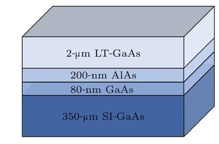
Fig.1. Structure of the epitaxial wafer.
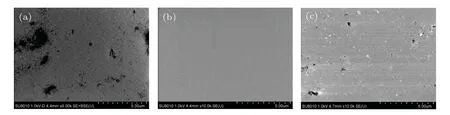
Fig.2. LT-GaAs thin films prepared by etching in(a)26.7%,(b)0.44%,and(c)13.57%HCl solutions.
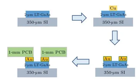
Fig.3.Flowchart for fabricating photoconductive LT-GaAs thin film antenna.
Under these conditions for obtaining high-quality LTGaAs thin films, the extent of bonding between the LT-GaAs thin film and silicon wafer was assessed. First, we fabricated a number of LT-GaAs thin film photoconductive antennas. A thin straight copper wire with a diameter of 200 µm was placed on the top of the silicon wafer with the LT-GaAs film and fixed with adhesive tape. Then they were inverted in a 2HD-400 high-vacuum evaporation coating machine (Beijing Taikenuo Technology Co.,Ltd.)to evaporate 20-nm-thick chromium layer and 250-nm-thick gold layer, sequentially.The Chromium evaporation was performed to improve the ad-hesion of the gold. After evaporation,the copper wire was removed,and the gold-plated components were the positive and negative poles of the antenna. To provide the appropriate voltage for the antenna,the gold electrode of the antenna and the copper electrode of a printed circuit board(PCB)were coated with an appropriate amount of conductive silver glue. The conductive tape was used to connect the components coated with conductive silver glue such that the gold electrode of the antenna and the copper electrode of the PCB were connected.Finally, the voltages of the positive and negative electrodes were connected to the PCB. We note that there was a hole in the middle of the PCB, through which a femtosecond laser could directly irradiate the gap between the electrodes; thus,the PCB did not affect the incident light,and it could not cause any loss of the terahertz wave. Figure 3 shows a flowchart of the process for producing the photoconductive LT-GaAs thin film antenna. The size of the whole photoconductive antenna was 4 mm×8 mm, while the size of LT-GaAs film on it was 2 mm×2 mm.
Next, two LT-GaAs thin film photoconductive antennas for generating and detecting the terahertz waves were placed in the terahertz asynchronous ultrafast time domain spectroscopy system with 800-nm-wavelength femtosecond laser as a light source in the testing experiment, and the time domain spectrum was obtained. It could be confirmed that the prepared LT-GaAs thin films have high quality,good transfer and bonding,and the thin film preparation scheme is feasible.
3. Investigation of LT-GaAs thin film photoconductive antennas
The above results show that the LT-GaAs thin films have suitable quality and bond well with the silicon wafers. Next,the LT-GaAs thin films were excited by a long-wavelength femtosecond laser at 1550 nm to determine whether they can generate terahertz waves. The test system is shown in Fig.4.
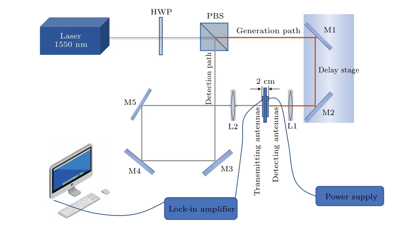
Fig.4. Diagram of terahertz test system.
The repetition rate of the laser was 100 MHz, and the pulse width was 75 fs. The femtosecond laser beam passed through a half wave plate (the power ratio of the two beams could be adjusted)and a polarization beam splitter.After passing through the polarization beam splitter,the laser beam was divided into two sub-beams.One sub-beam passed through the translation stage (M1/M2) and focused on the LT-GaAs thin film antenna through lens L1,which had a focal length of 5 cm.The other sub-beam focused on the LT-GaAs thin film antenna through reflectors M4 and M5 and lens L2,which had a focal length of 5 cm. Two thin film antennas were placed back-toback with one side of the electrode structure facing outward.A pulse voltage with a frequency of 10 kHz was applied to the antenna at the generating end,with a voltage of 100 V.When a DC bias voltage was applied across the electrodes of the photoconductor, the carriers were accelerated by the electrostatic field to generate ultrafast current pulses,which could be radiated to free space through the terahertz antenna.[19]The electrode of the detecting thin film antenna was connected with the lock-in amplifier, and the frequency of the lock-in amplifier was set to be 10 kHz. The laser power of the generating optical path and the detecting optical path were both approximately 10 mW and the distance between the two antennas was 2 mm. To achieve terahertz generation and detection,the repetition frequency of the AC voltage had to be the same as that of the phase-locked amplifier.[20]
A terahertz signal with a high signal-to-noise ratio was obtained in multiple experiments.Based on these experiments,figure 5 presents a time domain spectrum, which shows that the signal-to-noise ratio exceeds 10, indicating a low level of noise. Figure 6 shows a frequency domain spectrum from the experiments, which demonstrates that the terahertz spectrum can reach 0.6 THz.Although 350-µm silicon wafer can absorb terahertz wave to a certain extent, figure 6 shows the relativeintensity of terahertz wave, so the existence of silicon wafer will not affect the experimental results. In this experiment,a 1550-nm femtosecond laser was used instead of an 800-nm femtosecond laser.The experimental conditions are looser and the cost is lower.

Fig.5. Time domain spectrum of terahertz signal.
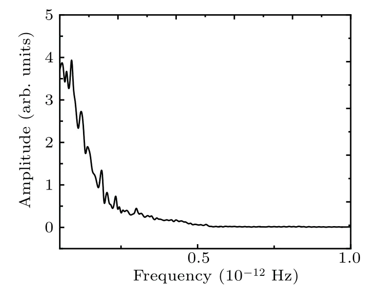
Fig.6. Frequency domain spectrum of terahertz signal.
The single photon energy of the 800-nm laser is 2.5 eV,whereas that of the 1550-nm laser is 0.8 eV.The band gap of LT-GaAs is 1.43 eV.Therefore,it is easy to generate the terahertz waves in LT-GaAs by an 800-nm femtosecond laser. In the experiment, we successfully excited the THz wave with 1550-nm laser. In Refs. [21–23], the non-quadratic dependence of optical conductivity and laser intensity was used to prove that the two-step photon absorption mediated by the intermediate band state formed by excess As (1%–2%) in LT-GaAs is helpful for photoconductivity, but not for twophoton absorption, at a relatively low excitation power value(<5 mW).In addition,we used HCl to etch different batches of epitaxial wafers to obtain the LT-GaAs thin films,and then fabricated thin film photoconductive antennas. After many tests,it was found that their performances are different.Therefore, it can be preliminarily considered that the preparation conditions and environment of LT-GaAs epitaxial wafers can also affect the intermediate band state.
4. Conclusions
In this work, we fabricate four-layer LT-GaAs substrate materials and cut them into 2 mm×2 mm pieces,and then the high-quality LT-GaAs thin films are obtained by etching the sacrificial layer of AlAs on the substrate with 13.57% HCl.Subsequently,the LT-GaAs thin film antennas are obtained by transferring,bonding,and welding electrodes,and the bonding of the films is evaluated in a terahertz asynchronous ultrafast time domain spectroscopy system in which an 800-nm femtosecond laser is used to excite and detect the terahertz waves.Finally,a terahertz time domain spectrum system is built,and the thin film antennas for generating and detecting the terahertz waves are investigated with a 1550-nm femtosecond laser. The corresponding time and frequency domain spectra are obtained,which proves that the LT-GaAs thin film antennas are feasible for generating and detecting terahertz waves. This work will expand the scope of applications of terahertz spectroscopy and lays the foundation for fabricating chips based on a terahertz time domain spectroscopy system, which is of great significance.
Acknowledgements
Project supported by the National Natural Science Foundation of China (Grant No. 61575131). The authors would like to thank Editage(www.editage.com)for English language editing.
猜你喜欢
Chinese Physics B(2022年11期)2022-11-21
小天使·一年级语数英综合(2022年4期)2022-04-28
医学概论(2022年3期)2022-04-24
快乐作文(1.2年级)(2021年2期)2021-09-10
快乐作文(1.2年级)(2021年6期)2021-07-26
快乐作文(1.2年级)(2021年12期)2021-03-21
北广人物(2019年48期)2019-12-18
陶瓷科学与艺术(2018年7期)2018-09-13
校园英语·上旬(2016年9期)2016-05-14
故事林(2007年2期)2007-05-14
- Chinese Physics B的其它文章
- High sensitivity plasmonic temperature sensor based on a side-polished photonic crystal fiber
- Digital synthesis of programmable photonic integrated circuits
- Non-Rayleigh photon statistics of superbunching pseudothermal light
- Refractive index sensing of double Fano resonance excited by nano-cube array coupled with multilayer all-dielectric film
- A novel polarization converter based on the band-stop frequency selective surface
- Effects of pulse energy ratios on plasma characteristics of dual-pulse fiber-optic laser-induced breakdown spectroscopy