
Temporal response of laminated graded-bandgap GaAs-based photocathode with distributed Bragg reflection structure:Model and simulation
2022-09-24 08:04ZiHengWang王自衡YiJunZhang张益军ShiManLi李诗曼ShanLi李姗JingJingZhan詹晶晶YunShengQian钱芸生FengShi石峰HongChangCheng程宏昌GangChengJiao焦岗成andYuGangZeng曾玉刚
Chinese Physics B 2022年9期
Zi-Heng Wang(王自衡) Yi-Jun Zhang(张益军) Shi-Man Li(李诗曼) Shan Li(李姗)Jing-Jing Zhan(詹晶晶) Yun-Sheng Qian(钱芸生) Feng Shi(石峰)Hong-Chang Cheng(程宏昌) Gang-Cheng Jiao(焦岗成) and Yu-Gang Zeng(曾玉刚)
1School of Electronic and Optical Engineering,Nanjing University of Science and Technology,Nanjing 210094,China
2National Key Laboratory of Science and Technology on Low-Level-Light,Xi’an 710065,China
3Changchun Institute of Optics,Fine Mechanics and Physics,Chinese Academy of Sciences,Changchun 130033,China
Keywords: temporal response,GaAs-based photocathode,distribution Bragg reflection,graded-bandgap
1. Introduction
Since the advent of the GaAs-based vacuum photocathode,it has attracted extensive research interest due to its high quantum efficiency,low thermal noise,spin-dependent effects,and high-speed response.[1-6]After decades of research, the GaAs-based photocathode gradually becomes irreplaceable in specific application areas,such as night vision imaging,spinpolarized electron source, spectrophotometer, photon counting, laser detection, and thermionic energy converters.[7-13]Quantum efficiency is one of the most significant parameters of photocathode. How to improve the quantum efficiency is always a hot issue in numerous photocathode researches.During this period, many approaches regarding structural design have been proposed, such as field-assist structure and distribution Bragg reflection (DBR) structure.[14-19]In previous researches, the photoemission process of the photocathode was treated as a steady-state situation for studying quantum efficiency or an unsteady-state situation for investigating temporal response.[20-23]For the field-assisted photocathode adopting the varied-doping structure,researchers have explored the temporal response characteristic theoretically and experimentally.[24,25]However, the dynamic temporal properties of the laminated GaAs-based photocathode with DBR structure and graded-bandgap emission layer still lack a suitable model to be described and investigated. Besides, the influence of the DBR structure on the temporal response and the intrinsic mechanism also need to be explained.
According to Spicer’s three-step model of photoemission,[26]the emission progress of excited electron can be divided into generation,transport and escaping. In the progress of photoelectron generation, the photocathode with gradedbandgap emission layer and DBR reflection layer has different photoelectron generation characteristics and electron transport characteristics. The DBR layer located beneath the emission layer can act as a reflector,which has the function of realizing the total reflection at target wavelength. Hence,the propagating process of the incidence light in the emission layer can be divided into two parts: forward incidence and backward reflection caused by the reflection of DBR structure. In addition, the interface recombination and built-in electric field in the laminated graded-bandgap emission layer also influence the internal transport of photoelectron. Accordingly,this laminated photocathode requires an appropriate time-dependent photoemission model.
In this paper, a time-dependent photoemission model is deduced to study the temporal response of the laminated GaAs-based photocathode with DBR structure and gradedbandgap emission layer. The derivation method is based on the unsteady one-dimensional continuity equations combined with the numerically discrete calculation. The related optical properties involved in the calculation process are simulated by the finite-different time-domain(FDTD)method. With the assist of the deduced model,the effect of the secondary absorption caused by the DBR layer and the graded bandgap structure on the temporal response are indicated clearly. We emphatically discuss the effect of DBR structure on the temporal response from the perspectives of emission layer thickness,electron concentration distribution,and incident light wavelength.The analysis results indicate that how the structural design of GaAs-based photocathode influences the temporal response,which will provide effective theoretical guidance for further improvement.
2. Structure and theoretical model
The laminated GaAs-based photocathode consists of a DBR layer,a varying-composition,and varying-doping emission layer. As shown in Fig.1(a),from top to bottom,the photocathode includes a GaAs-based emission layer, a DBR reflection layer,and a substrate.The emission layer is composed of the varying-composition and varying-doping InxGa1-xAs.Under the emission layer, the DBR layer is formed by alternately stacking two types of thin materials with different refractive indexes. Through reasonable design, the DBR layer has the function of realizing the total reflection at a specific wavelength.In this case,the original transmission light toward the substrate would be reflected back to the emitting layer,and thus generating the secondary absorption,which improves the absorptivity of the emission layer, especially the absorptivity at the target wavelength.
The energy band structure of the GaAs-based photocathode is shown in Fig.1(b). Because of the varying-composition and varying-doping structure, the conduction-bandECand valence-bandEVof the emission layer are respectively bent and inclined by the Fermi level leveling effect. Hence, the built-in electric fieldEinis generated in the bandgap bending region, and the direction is from the surface toward the bulk. With the assist of the built-in electric field and diffusing effect, the photoelectron transports toward the surface of the emission layer and finally enters into the vacuum. The DBR layer,which is composed of the alternating growing GaAs sublayer and AlAs sublayer, is grown on the high-quality GaAs substrate. The material of DBR structure guarantees the lattice matching at each interface. In addition,the AlAs sublayer also has the function of preventing the reverse recombination of photoelectron,because of the broad bandgap. In structural design,the emission layer is divided intonsublayers,and the In composition of each sublayer gradually increases in the direction of electron transport. The doping concentration of the emission layer exponentially decreases in the direction of electron transport.

Fig. 1. (a) Structure diagram and (b) energy band structure of laminated GaAs-based photocathode,with EC being the minimum of conduction band,EV the maximum of valence band,EF the Fermi level,E0 the vacuum level,and Ein the built-in electric field.
According to the theory of thin film optics,the thickness of the alternating materials needs satisfy the following expressions to realize the total reflection at target wavelength:

whereλtargetis the target wavelength,nLandnHare the refractive indices of the materials in the DBR layer respectively,andnH>nL,dLanddHare the thicknesses of these two materials in each alternation period. When the In composition changes linearly,the intensity of the built-in electric field generated by the varying-composition and exponential-doping can be calculated by the following formulas:[14,27,28]

whereN(Tn) andN(0) are the doping concentrations at the ends of the emission layer,k0is the Boltzmann constant,Tkthe absolute temperature,q0the electron charge,EgnandEg1are the bandgaps of the innermost sublayer and the outmost sublayer in the emission layer,andTnis the total thickness of the emission.
The unsteady one-dimensional continuity equation of the laminated GaAs-based photocathode can be expressed as

wherene(z,t) is the instantaneous electron concentration in the emission layer,Dniis the electron diffusion coefficient,µiis electron mobility,τiis the lifetime of electron,and the subscriptivalue runs from 1 ton,corresponding to the sublayers with different In compositions in the emission layer.When the incident light transmits through the emission layer at the first time,the light absorption process is called first absorption,and the generation rate of photoelectronsg1(z,t)can be expressed as given below. Whent=0,

whereRhvis the reflectivity of incident surface,I0is the intensity of incident light,αhvis the absorption coefficient,diis the thickness of each sublayer,andTiis the position of a sublayer along thezaxis. Because the DBR layer is located behind the emission layer, the transmission part of the incident light will be reflected back into the emission layer and causes the secondary absorption in the emission layer. At this point,the photoelectron generation rate of the secondary absorption can be expressed below. Whent=0,

whereTemissionis the transmissivity of the emission layer,RDBRis the reflectivity of the DBR layer, andR'hvis the reflectivity of the emission layer in the backward direction. To solve the differential continuity equation, Eq. (7), the boundary conditions of the interfaces between the sublayers are also necessary,and the equations are given as follows:wheni=2,3,...,n,

wheretsis the average decay time of the electron concentration at the emitting surface,which is an approximately comprehensive parameter describing the whole photoelectron transport progress,[24]andSviis the surface recombination rate of each interface. To investigate the time response characteristic of the photocathode,it is assumed that the light source is an ideal pulse source att=0. Hence,the continuity equation,Eq.(7),is given below.whent/=0,

Since the exact analytical solution of the unsteady continuity equation cannot be obtained easily through the above equations,the differential discrete method of numerical calculation is utilized to approximate to the actual solution. In this way,the thicknesses of the emission layer and the time lapsing can be discretized into grids. The thickness is divided intoMparts and each spatial step is Δz. The time lapsing is divided intoKparts and each temporal step is Δt. In this case, the electron concentration distribution in the emission layer can be discretized as follows:
whereNis the discretized electron concentration distribution,jis the discretized spatial coordinate,kis the discretized temporal coordinate. Afterward, the continuity equation and boundary conditions can also be represented by the discretized method. Whent=0,the initial value of the electron concentration distribution becomes

3. Simulation and discussion
The model of the temporal response characteristic of the laminated GaAs-based photocathode is deduced by numerically solving the unsteady one-dimensional continuity equation. In this case, the relationship between the structural design and the temporal response characteristic can be further investigated through the deduced model. The structural parameters of the photocathode are set to be as follows. The InxGa1-xAs emission layer is divided into 5 sublayers with different In compositions. The thickness values of sublayers each are 0.1µm, 0.1µm, 0.1µm, 0.1µm, and 0.7µm, from bulk to surface,and the In composition values of corresponding sublayers are 0.05, 0.10, 0.15, 0.20, 0.20, respectively.The doping concentration of the entire emission layer exponentially decreases from 1×1019cm-3to 1×1018cm-3,from bulk to surface. Under the ideal assumption, the In composition in the emission layer increases linearly from 0.05 to 0.20 within a thickness of 0.4 µm. Afterwards, a uniform composition In0.2Ga0.8As sublayer of 0.7 µm in thickness adjacent to the varying composition sublayers helps to improve the absorption capability at 1064 nm. For computability, it is assumed that the bandgap changes linearly in the varying composition region. In this case, the built-in electric fieldE2generated by the varying composition is considered to be uniform in the varying composition region.[27,28]Since the outmost and second sublayers are both In0.2Ga0.8As material,it is considered that there is no interface between the two sublayers in simulation. Therefore,the photoelectrons in the second sublayer directly travel across the interface into the outmost sublayer without recombination. In simulation, the refractive index and extinction coefficient of GaAs and AlAs are cited from Ref. [29], while the refractive index and extinction coefficient of InxGa1-xAs are taken from Ref. [30]. According to Eqs.(1)and(2), to reduce the reflectivity and improve the photoresponse at 1064 nm, the thickness values of the GaAs and AlAs in the DBR layer are set to be 76 nm and 90 nm,respectively. The quantity cycle of the DBR layer is set to be 10 and the total thickness of the DBR layer is 1.66µm. Because the propagation time of the incident light in the emission layer and the DBR layer is much less than the temporal response of photocathode, the propagation time is ignored in the simulation. In this case, the optical properties of the photocathode with the mentioned structural design can be simulated to verify the reasonability. As shown in Fig. 2, the FDTD method is utilized to theoretically calculate the reflectivity and the absorptivity spectrum of the photocathode with the above structure. In the process of FDTD simulation, the light source is placed in the vacuum,and the light beam is incident normally on the surface of emission layer.As shown in Fig.2,the reflectivity curve appears as an oscillating curve in the wavelength range above 800 nm, because of the alternant thin films. According to the theory of DBR design, the lowest wavelength valley when the reflectivity curve fluctuates should be located at 1064 nm. The simulated reflectivity curve and absorptivity curve reach a minimum value and a maximum value at 1064 nm, respectively, which proves that the introduction of DBR structure reliably can improve the absorption capability of emission layer at 1064 nm.
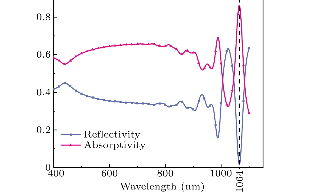
Fig. 2. Simulated reflectivity curve and absorptivity curve of the InxGa1-xAs emission layer with DBR structure.
Combining the results of FDTD simulation,the temporal response of the photocathode can be calculated by the deduced model. As for the varying-composition InxGa1-xAs emission layer, the band gap, electron mobility, electron diffusion coefficient all depend on In compositionx, and the relationship expressions are given by[31,32]


Table 1. Parameters used in simulation of quantum efficiency curves.

Fig. 3. Simulated flux curves of emitted photoelectrons with (a) different surface electron decay time ts and(b)different thickness values of uniform composition In0.2Ga0.8As sublayer.
The flux curves of emitted photoelectron with different values oftsare simulated and shown in Fig. 3(a), wherein the total thickness of InxGa1-xAs emission layer is set to be 1.1 µm. The wavelength of monochromatic pulse light source is 1064 nm. It can be seen obviously that with the increase ofts, the positions of the peak values severely shift to the right and the full widths at half maximum(FWHM)are broadened. According to the definition, in a certain photocathode structure, the value oftsshould also be determined.Changing the value oftsalone can lead to discrepancies in the simulation results as shown in Fig. 2(a). The value oftsis relevant to the whole photoelectron transport process, especially the thickness of emission layer. In this case, the value oftsis determined by the thickness of emission layer and the relationship is cited from the results of Ref.[24]. The normalized flux curves of emitted photoelectrons with different thicknesses of emission layer are simulated and shown in Fig.3(b). Because the uniform composition In0.2Ga0.8As sublayer is the main part of the emission layer, and has the best absorption at 1064 nm,the thickness of the uniform composition In0.2Ga0.8As sublayerd1is adjusted in simulation. It can be seen that the increase of the thickness significantly worsens the temporal response in terms of the right shift of peak and the broadening of FWHM, as shown in Fig. 3(b). With the increase of thickness of the uniform composition sublayer,more photoelectrons are generated in the deeper region,which weakens the enhancement of DBR layer. Besides, the photoelectrons need more transit time to reach the emitting surface.
Although the graded-bandgap emission layer and the DBR layer can improve the quantum efficiency, the effect of this laminated structure on the temporal characteristic still needs further studying. Figure 4(a)demonstrates the normalized flux curves of emitted photoelectrons for the varying composition structure and the uniform composition structure. In the simulations, the total thickness of InxGa1-xAs emission layer in the structure with DBR layer is set to be 1.1 µm. In the comparative structure,the entire emission layer is replaced by a uniform In0.2Ga0.8As layer with the same thickness. Besides,tsis set to be 2.4 ps for both structures.[24]It can be clearly observed that the photocathode with graded-bandgap emission layer has better temporal response,because the builtin electric field which is opposite to the direction of electron movement,accelerates the movement of electrons. To reduce the influence of structural difference on the result, the temporal response of the proposed structure is simulated without considering the built-in electric field for comparison. The improvement effect of the built-in electric field on the temporal response can be directly observed. According to the above deduced photoelectron generation rate formula,the existence of DBR layer improves the problem of diffusion velocity by the distributing of the generated electrons. Through the abovededuced model of electron concentration distribution, it can be found that the effect of secondary absorption of DBR layer is determined by the thickness of emission layer. Too thick an emission layer will reduce the light energy entering into the DBR layer and weaken secondary absorption. To verify this conjecture, a new photocathode structure with thinner emission layer is simulated for comparison as shown in Fig.4(b).In this new structure, the total thickness of emission layer is set to be 0.6 µm, and the thickness of the uniform composition In0.2Ga0.8As sublayer decreases to 0.2 µm for reducing the light absorption in the first absorption. Meanwhile, thetsis adjusted to 1.5 ps due to the decrease of emission layer thickness.[24]It can be seen that the improvement effect of the DBR layer on the temporal response becomes more obvious with emission layer thinening, because the proportion of the excited electrons generated by the secondary absorption increases with the thickness of emission layer decreasing.
Figure 5 shows the time evolutions of the electron concentration distributionn(z,t)in the emission layers with different photocathode structures. The total thickness of the emission layer is set to be 0.6µm to emphasize the effect caused by the DBR structure,andtsis assumed to be 1.5 ps.The emitting surface is located at the origin of abscissa. In Fig. 5(a), it is clear that the initial photoelectron distribution is uniformized by the secondary absorption because of the DBR structure.With the emitting of photoelectron,the electron concentration at the emitting surface decreases rapidly,and a bulge of electron concentration distribution is formed in the bulk as shown in Figs. 5(b)-5(d). In this case, the uniform initial electron concentration distribution can reduce the blocking effect of concentration gradient on photoelectron diffusion. The electron concentration in the In0.15Ga0.85As sublayer decreases faster, due to a mass of photoelectrons passing through the interface between In0.2Ga0.8As sublayer and In0.15Ga0.85As sublayer,and transporting toward the emitting surface. Meanwhile,these figures also demonstrate the characteristics of the DBR layer to enhance the absorption capacity of the emission layer.

Fig. 4. Simulated flux curves of emitted photoelectrons for (a) different built-in electric field cases and(b)different emission layer thickness values with or without DBR layer.
Figure 6 shows the relationship between the DBR structure and temporal response under different incident light wavelengths. The total thickness of emission layer is also 0.6 µm andtsis also set to be 1.5 ps. It is noted that the improvement effect of DBR structure on the temporal response is obvious for the 1064-nm-wavelength incident light, while the temporal response of the photocathode with DBR structure is no different from that without DBR structure for the 780-nm-wavelength incident light. Besides, it can also be found that the improvement effect of DBR structure on the temporal response is reduced when the incident light wavelength decreases. Because the InGaAs material has weaker absorption capability for the longer wavelength light,with the wavelength of incident light decreasing,less transmission light can reach the DBR layer and establish the secondary absorption.However,the improvement effect of the DBR structure is determined by the contribution of secondary absorption to total absorption. After the incident light is absorbed completely in the first absorption process,the introduction of DBR layer has no influence on the temporal response.
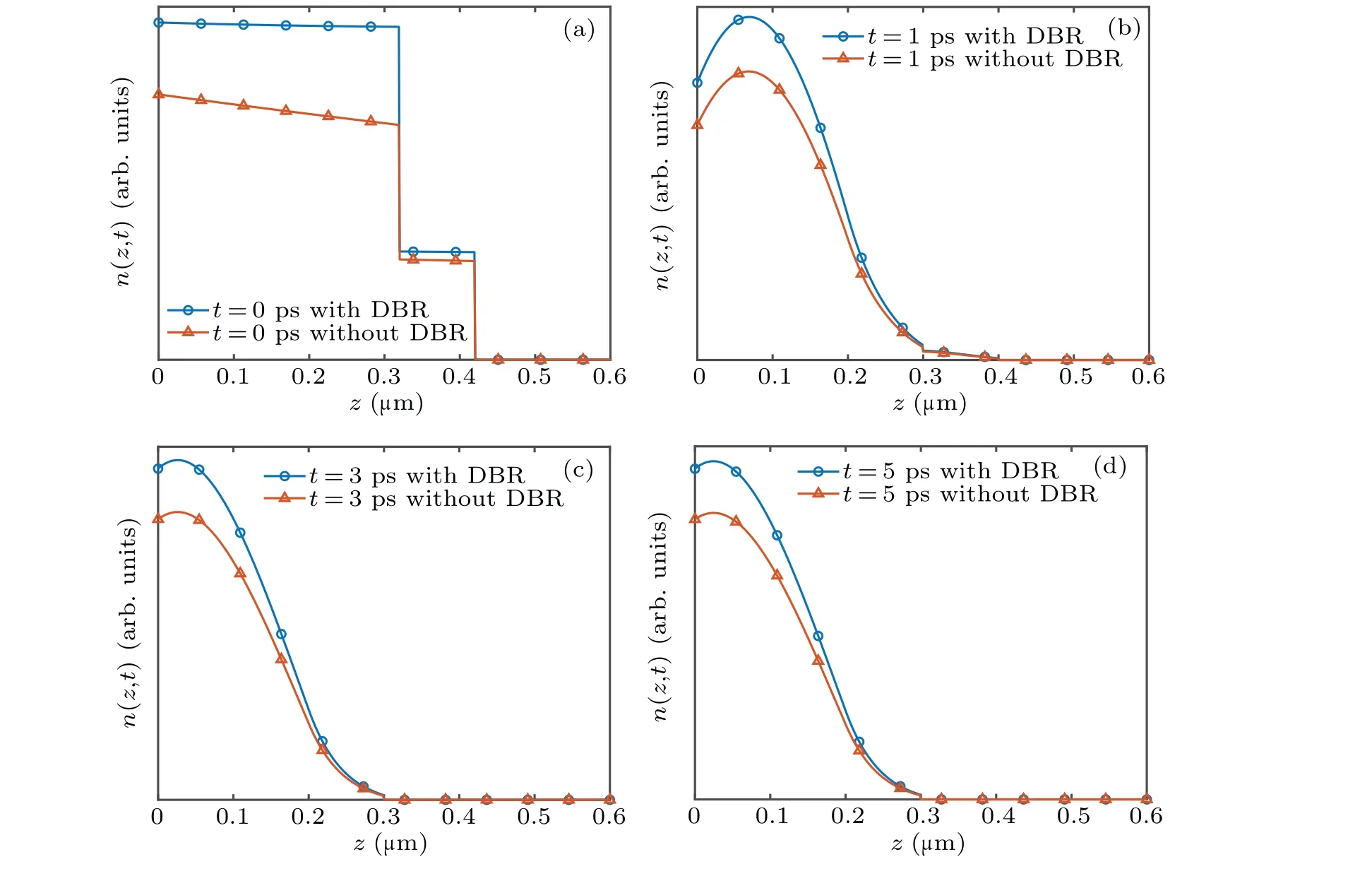
Fig.5. Electron concentration distributions in emission layer with and without DBR at time t=0 ps(a),1 ps(b),3 ps(c),and 5 ps(d).

Fig.6. Simulated flux curves of emitted photoelectrons in emission layer with and without DBR at incident light wavelength of(a)1064 nm,(b)960 nm,and(c)780 nm.
4. Conclusions
In this work, a general theory model is deduced to describe the temporal response of the laminated graded-bandgap GaAs-based photocathode with DBR structure.By solving the unsteady continuity equation through numerical computation method, the time-dependent flux of emitted photoelectrons is obtained. Besides, the relationship between the temporal response and the structural parameters including the thickness of emission layer,the built-in electric field and the DBR structure is explored. Meanwhile, the time evolution of electron concentration distribution in the emission layer and the influence of incident light wavelength on the temporal response are also simulated. Through the DBR layer, the discrepancy between the absorption capability of the emitting layer and the temporal response can be resolved. By adjusting the initial electron concentration distribution, the temporal response is improved, with the of DBR layer introduced. Moreover, the improvement effect of the DBR layer on the temporal response is enhanced with the decrease of emission layer thickness or the increase of the incident light wavelength. This theoretical model of temporal response characteristic of the complicated GaAs-based photocathode will contribute to the optimization of cathode structure for near infrared response.
Acknowledgements
Project supported by the National Natural Science Foundation of China(Grant Nos.U2141239 and 61771245)and the Fund from the Science and Technology on Low-Light-Level Night Vision Laboratory of China(Grant No.J20200102).
猜你喜欢
中国典型病例大全(2022年12期)2022-05-13
疯狂英语·新悦读(2021年5期)2021-06-08
阅读(快乐英语高年级)(2021年2期)2021-04-26
阅读(快乐英语中年级)(2020年11期)2020-12-28
影剧新作(2020年4期)2020-12-04
作文评点报·低幼版(2020年32期)2020-07-23
青年生活(2019年3期)2019-09-10
实践·党的教育版(2018年7期)2018-08-30
艺术评论(2016年9期)2016-11-10
云南画报(2015年2期)2015-05-04

- Chinese Physics B的其它文章
- Characterizing entanglement in non-Hermitian chaotic systems via out-of-time ordered correlators
- Steering quantum nonlocalities of quantum dot system suffering from decoherence
- Probabilistic quantum teleportation of shared quantum secret
- Spin–orbit coupling adjusting topological superfluid of mass-imbalanced Fermi gas
- Improvement of a continuous-variable measurement-device-independent quantum key distribution system via quantum scissors
- An overview of quantum error mitigation formulas