
Ozone oxidation of 4H-SiC and flat-band voltage stability of SiC MOS capacitors
2022-11-21 09:38ZhiPengYin尹志鹏ShengShengWei尉升升JiaoBai白娇WeiWeiXie谢威威ZhaoHuiLiu刘兆慧FuWenQin秦福文andDeJunWang王德君
Chinese Physics B 2022年11期
Zhi-Peng Yin(尹志鹏) Sheng-Sheng Wei(尉升升) Jiao Bai(白娇) Wei-Wei Xie(谢威威)Zhao-Hui Liu(刘兆慧) Fu-Wen Qin(秦福文) and De-Jun Wang(王德君)
1Key Laboratory of Intelligent Control and Optimization for Industrial Equipment,Ministry of Education;School of Control Science and Engineering,Faculty of Electronic Information and Electrical Engineering,Dalian University of Technology,Dalian 116024,China
2State Key Laboratory of Materials Modification by Laser,Ion,and Electron Beams(Ministry of Education),Dalian University of Technology,Dalian 116024,China
We investigate the effect of ozone (O3) oxidation of silicon carbide (SiC) on the flat-band voltage (Vfb) stability of SiC metal–oxide–semiconductor (MOS) capacitors. The SiC MOS capacitors are produced by O3 oxidation, and their Vfb stability under frequency variation, temperature variation, and bias temperature stress are evaluated. Secondary ion mass spectroscopy(SIMS),atomic force microscopy(AFM),and x-ray photoelectron spectroscopy(XPS)indicate that O3 oxidation can adjust the element distribution near SiC/SiO2 interface,improve SiC/SiO2 interface morphology,and inhibit the formation of near-interface defects, respectively. In addition, we elaborate the underlying mechanism through which O3 oxidation improves the Vfb stability of SiC MOS capacitors by using the measurement results and O3 oxidation kinetics.
Keywords: SiC MOS capacitors,ozone oxidation,bias temperature instability,Deal–Grove model
1. Introduction
Silicon carbide (SiC) and gallium nitride (GaN) materials are the third-generation semiconductors. However, unlike the application of GaN device in high frequency field,[1–4]SiC power device is more favored in the field of high temperature and high voltage due to its wide bandgap, high breakdown field strength,high thermal conductivity,and high compatibility with the Si process.[1,2]However, the low channel mobility and threshold voltage(Vth)instability of SiC metal–oxide–semiconductor field-effect-transistor (MOSFET) device seriously limit its development.[3,4]After decades of research,although the channel mobility of SiC MOSFET device has been improved to an acceptable level via the nitric oxide(NO)postoxidation annealing (POA) process,[5,6]theVthinstability of SiC MOS capacitor is still a serious problem to be solved.[7]TheVth/flat-band voltage(Vfb)instability is mainly due to the interface trap and near interface oxide trap (NIOT) formed near the interface during traditional dry oxidation.[8–10]
These defects can be eliminated by POA and improved oxidation processes;[5,11–13]the latter can suppress the generation of these defects fundamentally by increasing the oxidant concentration near the SiC/silicon dioxide (SiO2)interface.[14–16]Improved oxidation processes include wet oxidation,[17]NO oxidation,[6]plasma oxidation,[18,19]and ozone (O3) oxidation.[20]Although these methods can reduce the interface trap density (Dit) of SiC MOS devices to some extent, wet oxygen, NO, and plasma oxidation may lead toVth/Vfbinstability,[21,22]the introduction of fast traps,[23]and sample damage due to highly energetic particle bombardment,[24]respectively. By contrast,O3oxidation can inhibit the generation of interface defects without the introduction of foreign elements.[25]It has a low manufacturing cost for SiC MOS devices because of its high compatibility with Si oxidation, and is more environment friendly than NO.[26]In 2003, Kosugiet al.reported that O3oxidation of SiC can reduce theDitof SiC MOS capacitors.[20]However,no further reports have been provided.
In this work, we investigate theVfbstability of SiC MOS capacitor produced by O3oxidation. TheVfbstability of SiC MOS capacitor via current–voltage (I–V) measurement at room temperature and capacitance–voltage(C–V)measurements at different test temperatures, test frequencies,and bias temperature stresses are evaluated. Subsequently,secondary ion mass spectrometry (SIMS), atomic force microscopy(AFM),and x-ray photoelectron spectroscopy(XPS)are used to test the element distribution, interface morphology, and interface element bonding near the SiC/SiO2interface,respectively. The underlying mechanism through which O3oxidation affects theVfbstability of SiC MOS capacitors is analyzed based on the measurement results and oxidation kinetics.
2. Experiment
The 4°off-axis n-type 4H-SiC substrates with 5-μm-thick epitaxial layers produced by Cree Inc.,were used in this experiment. The epitaxial layers were doped with N concentration of 1×1016cm-3. The substrates were cleaned successively in acetone, ethanol, and deionized water via ultrasonic cleaning and immersed in 15% hydrofluoric acid (HF) buffer solution for 10 min to remove the natural oxide layer. Subsequently,the substrates were subjected to Radio Corporation of America standard cleaning and dried under the protection of N2.The O3oxidation of SiC was carried out separately at oxidation temperatures of 1100°C,1150°C,and 1200°C to obtain 35-nm SiO2films.
The oxidant was O3/O2mixed atmosphere with an O3concentration of 150 mg/L;it was produced via dielectric barrier discharge in high-purity O2. Meanwhile,control samples were oxidized in high-purity O2atmosphere at 1200°C to obtain 30-nm-thick SiO2films.All samples were annealedin situin N2for 30 min. After removing the oxide film on the back of the samples, we evaporated aluminium (Al) on the front and back of each sample to create a gate electrode and back electrode, each with a diameter of 200 μm, respectively. The SiC MOS capacitors were prepared after electrodes have been metallized in N2atmosphere.
The Keithley 4200 semiconductor characterization system was used to evaluate the electrical characteristics of the various SiC MOS capacitors. TheI–Vmeasurement was performed to test the insulation characteristics of SiO2films on SiC. TheC–Vcurves were extracted with different frequencies in a range from 10 kHz to 5 MHz at room temperature to study the frequency dispersion of the various SiC MOS capacitors. Subsequently,the temperature dependence of theVfbof the SiC MOS capacitors was analyzed by using theC–Vcurves tested under different temperatures(from 80 K to 300 K).After exerting the positive and negative bias temperature stress(PBTS and NBTS), theC–Vcurves were measured at 100,150,200,and 300 K,and the stress value and stress time were±2.5 MV/cm and 600 s, respectively. The bias temperature instability(BTI)of the various SiC MOS capacitors was evaluated by using the difference(ΔVfb)between theVfbvalues of theC–Vcurves after having exerted positive stress and negative stress. In addition,DitandNotwere extracted to study the mechanism through which O3oxidation affects theVfbstability of SiC MOS capacitors.
The element distribution near the SiC/SiO2interface can considerably affect the type of defect near the SiC/SiO2interface. To understand the influence of O3oxidation on the element distribution near the SiC/SiO2interface,we performed the SIMS measurement of the SiC/SiO2structures to obtain the depth profile of Si, carbon (C), and O elements. The SiC/SiO2interface morphology and the chemical bonding state of interfacial Si and C were extracted through AFM and XPS,respectively. XPS Si 2p and C 1s spectra were obtained by using the PHI Quantera II system with a monochromatic Al Kαsource(hν=1486.6 eV).The results were utilized to evaluate the interface quality of different samples. In addition,the kinetics of O3oxidation was analyzed based on the modified Deal–Grove model presented by Yoshiokaet al.[27]The model was combined with the measurement results to elucidate the underlying mechanism of the effect of O3oxidation on theVfbstability of SiC MOS capacitors.
3. Results and discussion
3.1. Breakdown characteristics of SiO2 films
Figure 1 shows theJ–Ecurves of the SiC MOS capacitors and the breakdown field strength(Eox)of the SiO2films.TheJ–Ecurves present the typical Fowler–Nordheim (FN)characteristics.[28]Although the leakage currents in the SiO2films of the various samples are similar in the soft breakdown region,obvious differences exist in theEoxof the various samples. We extract theEoxvalues of different samples as shown in Fig. 1(b). TheEoxincreases with the rise of O3oxidation temperature,indicating that O3oxidation at high O3oxidation temperatures in a range of 1100°C–1200°C can produce SiO2films with good insulation characteristics. Compared with the SiO2films prepared via dry oxidation at the same oxidation temperature(1200°C),the samples prepared by O3oxidation has a largerEox. This result indicates that the O3oxidation can produce SiO2films with good insulation characteristics,which is the precondition to achieve goodVfbstability in SiC MOS devices.[29]

Fig.1. (a)The J–E curves and(b)Eox versus oxidation temperature of various SiC MOS capacitors,with dotted lines representing Eox of SiO2 film of the control sample.
3.2. Frequency dispersion
As shown in Fig.2,we extract theC–Vcurves of the SiC MOS capacitors at different frequencies ranging from 10 kHz to 1 MHz. TheC–Vcurves of all the samples gradually shift toward the accumulation region with the increase in test frequency;this phenomenon is called frequency dispersion.[30,31]We observed that large frequency dispersion leads to an obviousVfbshift,that is,Vfbinstability of the SiC MOS capacitors is induced by test frequency variation. As shown in Fig. 2,the frequency dispersions of the various SiC MOS capacitors are similar, which may be due to the similar number of slow traps in capacitors. This situation makes qualitative comparison difficult,so we extract the values ofVfbof theC–Vcurves tested under different frequencies for a quantitative comparison. Given that theVfbtested at 10 kHz is the smallest, we adopted it as the reference value in the quantitative calculation. ΔVfb-10Kwas obtained from the following equation:

whereVfb-Fis theVfbtested at different frequencies, andVfb-10Kis theVfbtested at 10 kHz.
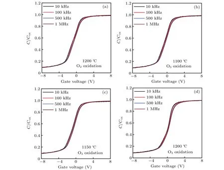
Fig.2. The C–V curves of various SiC MOS capacitors under different test frequencies.
From Fig. 3, we observed that ΔVfb-10Kdecreases with the increase in O3oxidation temperature, indicating that the higher the O3oxidation temperature is, the better theVfbstability of the SiC MOS capacitors is during test frequency variation.Moreover,the sample formed by O3oxidation at 1200°C has a smaller ΔVfb-10Kthan the control sample. This finding signifies that the SiC MOS capacitor oxidized by O3at 1200°C has betterVfbstability during test frequency variation than those oxidized by O2at the same temperature. We notice that the ΔVfb-10Kof the control sample is similar to that of the sample oxidized by O3at 1150°C.TheVfbstability during test frequency variation of the sample obtained by dry oxidation at 1200°C is only similar to that of the sample obtained by O3oxidation at 1150°C.
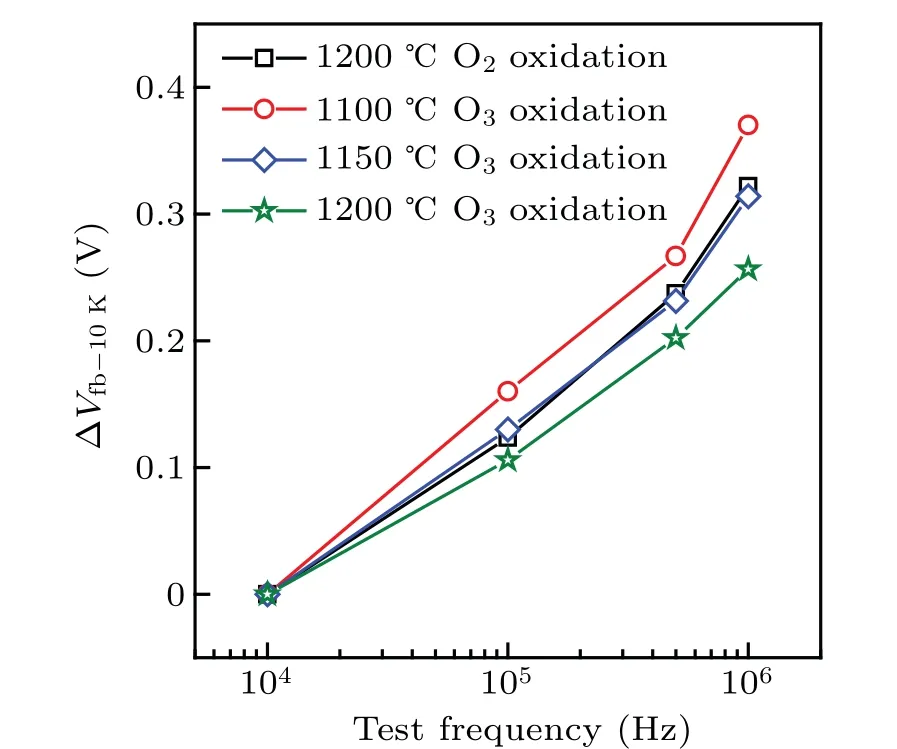
Fig.3. Curves of ΔVfb-10 K versus test frequency of various SiC MOS capacitors.
3.3. Effect of test temperature on Vfb
Figure 4 shows our measuredC–Vcurves of the SiC MOS capacitors in a temperature range of 80 K–300 K with a test frequency of 1 MHz. TheC–Vcurves shift toward the accumulation region with the test temperature decreasing, which leadsVfbto shift. We extract ΔVfb-300Kfrom the following formula:

whereVfb-Tis theVfbat temperatureT, andVfb-300Kis theVfbat 300 K.The results are shown in Fig.5(a). We find that ΔVfb-300Kdecreases with the increase in O3oxidation temperature. This result indicates that the increase of O3oxidation temperature can improve theVfbstability of SiC MOS capacitors against test temperature variations. In addition,when the test temperature changes, the SiC MOS capacitors obtained by O3oxidation at 1200°C show betterVfbstability than those formed by dry oxidation. Liuet al.reported that low temperature can reduce the difference between Fermi level (Ef)and the bottom of conduction band (Ec), so many interface traps nearEcare occupied by carriers with the decrease in temperature,[32]leadingVfbto shift. This result also means that a smallDitcan provide goodVfbstability under test temperature variations. Subsequently,we calculatedDitin a range of 0.06 eV–0.18 eV under the values ofEcfor various samples by using the Gray–Brown method.[33,34]
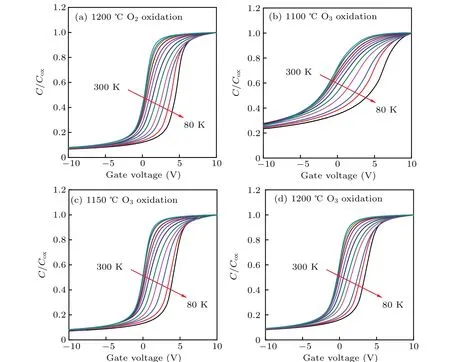
Fig.4. The C–V curves of various SiC MOS capacitors under test temperatures in a range of 80 K–300 K.

Fig.5. Curves of(a)ΔVfb-300 K versus test temperature and(b)Dit versus(Ec–E)for SiC MOS capacitors prepared at four different temperatures.
As shown in Fig.5(b),Ditin a range of 0.06 eV–0.18 eV decreases continuously with the increase in O3oxidation temperature. Compared with theDitof the control sample,theDitof the samples obtained by O3oxidation at the same temperature is reduced by nearly three quarters. TheDitof the control sample is only comparable to that of the samples formed by O3oxidation at 1150°C. This result indicates that O3oxidation can effectively suppress the generation of interface traps at the SiC/SiO2interface, thereby improving theVfbstability of SiC MOS capacitors.
3.4. The Vfb stability under BTS
TheVfbBTI of the SiC MOS capacitor is studied by testing the post-BTSC–Vcurves in a temperature range of 100 K–300 K. TheC–Vcurves of post-BTS are shown in Figs. S1–S4 in supporting information. We extract the difference(ΔVfb)inVfbbetween post-positive-stress and post-negative-stressC–Vcurves, as shown in Fig. 6(a). We find that ΔVfbincreases with the decrease in test temperature for two reasons. First,many interface traps and NIOTs can be occupied by electrons due to the decrease in the difference betweenEfandEc, resulting from the decrease in test temperature.[9,34]Second, a low temperature can reduce the de-trapping rate of trapped carriers.[9,35]Therefore, the electrical signals of many traps can be tested byC–Vcurves. We observed that ΔVfbdecreases with the increase in O3oxidation temperature,indicating thatVfbBTI can be effectively improved by O3oxidation at high temperatures. In addition, we discovered that the ΔVfbof the control sample is similar to that of the sample obtained by O3oxidation at 1100°C. TheVfbstability of the control sample was only comparable to that of the sample obtained by O3oxidation at 1100°C;it is obviously worse than that of the sample obtained by O3oxidation at 1200°C. We realized that compared with dry oxidation,O3oxidation can be used to prepare SiC MOS capacitors with betterVfbstability. Sunet al.reported that a linear relationship exists between the difference(ΔVmg)ofVmgbetween post-positive-stress and post-negativestressC–Vcurves and the sum of mobile ions and oxide trap charges.[35]When they conductC–Vtests at low temperatures,the mobile ions hardly move, leading to a minimal influence on ΔVmg.[9,36]Therefore, ΔVmgonly has a linear relationship with the oxide trap charge at low temperatures. We extract the values of ΔVmgof the various SiC MOS capacitors for a quantitative analysis of NIOTs. As shown in Fig. 6(b), ΔVmgdecreases with the increase in the O3oxidation temperature.

Fig.6. Test temperature-dependent(a)ΔVfb,(b)ΔVmg,and(c)Not for SiC MOS capacitors prepared at four different temperatures.
Subsequently, we calculate the oxide trap amount (Not)from the following equation:[25,35]
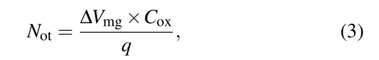
whereCoxis the oxide capacitance per unit area andqis the elementary charge. As shown in Fig.6(c),we find thatNotdecreases with the increase in O3oxidation temperature, which means that SiC MOS capacitors with lowNotcan be prepared at a high O3oxidation temperature. In addition,we notice that theNotof the control sample is similar only to that of sample obtained by the O3oxidation at 1100°C and larger than that of sample obtained by the O3oxidation,separately,at 1150°C and 1200°C.This result indicates that compared with dry oxidation,the O3oxidation can produce the SiC MOS capacitor with lowNot,thereby improving theVfbstability of SiC MOS capacitor.
According to the measurement results,the SiC MOS capacitor with similarVfbstability can be produced by the O3oxidation at lower oxidation temperature than by the dry oxidation. A high O3oxidation temperature can effectively improve theVfbstability of SiC MOS capacitor in a temperature range of 1100°C–1200°C.In addition,O3oxidation can produce SiC MOS capacitor with lowerDitandNotthan by dry oxidation,thereby improving theVfbstability of SiC MOS capacitor.
3.5. Element distribution near SiC/SiO2 interface
Figure 7 shows the results of SIMS measurement,namely,the element distributions near the SiC/SiO2interfaces of different samples. The blue, black, and green dotted lines in Fig.7 represent the boundary of the SiO2bulk, the SiC/SiO2interface,and the boundary of the SiC bulk,respectively.[34,37]The area between the SiO2bulk boundary and the SiC/SiO2interface represents the interface-transition region.[37]The peak of Si element content is observed in a part of the area between the SiC/SiO2interface and the boundary of the SiC bulk, which is called the Si-rich region and marked by red dotted lines in Fig.7.[34]Previous reports have indicated that many defects exist in the interface-transition region and Sirich region,[38]and they can influence theVfbstability of SiC MOS capacitor by forming interface traps or NIOTs.[11,39–41]Therefore,studying the element distributions in these regions is essential to evaluate the possibility of defects.
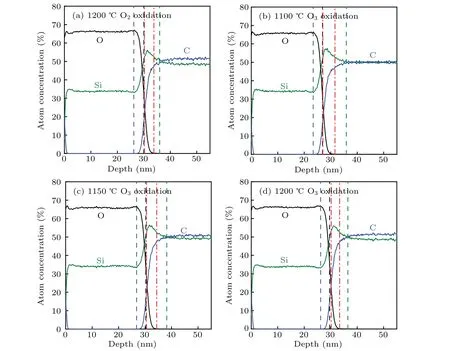
Fig.7. Si,C,and O element depth profiles of various SiC/SiO2 structures.
We extracted the thickness of the interface-transition and Si-rich region. Figure 8(a) shows the thickness of the interface-transition region in the different samples formed by O3and dry oxidation. The black dashed arrow in Fig. 8(a)indicates the thickness of the interface-transition region in the control sample. In addition,we calculate the relative Si and C element contents in the interface-transition region of the different samples, and the results are shown in Fig.8(b). The blue and black dotted arrows represent the relative Si and C element contents in the interface-transition region of the control sample,respectively. As presented in Figs.8(a)and 8(b),by comparing thickness and relative Si and C element contents of the interface-transition region of various samples, we examined the effect of O3oxidation on the interface-transition region.On the one hand, the thickness and relative Si and C element contents of the interface-transition region formed by O3oxidation are smaller than those of the interface-transition region formed by dry oxidation. On the other hand,the thickness and relative Si and C element contents of the interface-transition region decrease with the increase in O3oxidation temperature in a range of 1100°C–1200°C. The interface-transition region of the sample obtained by O3oxidation at 1200°C is the thinnest, and its thickness is approximately 0.4 nm less than that of the samples formed by dry oxidation at the same oxidation temperature. Given that a thin interface-transition region and low Si and C element contents in the interfacetransition region can reduce the existence possibility of Si-and C-related defects in the interface-transition region,[42]we infer that O3oxidation can suppress the formation of defects in the interface-transition region.
Figure 8(a)also shows the thickness of the Si-rich region in various samples. The blue dashed arrow in Fig. 8(a) indicates the thickness of the Si-rich region in the control sample.Figure 8(c)shows the Si and C element contents in the Si-rich region of different samples; the blue and black dotted arrows represent the Si and C element contents in the Si-rich region of the control sample, respectively. We notice that O3oxidation at high oxidation temperatures reduces the thickness of the Si-rich region and the relative Si and C element contents in the Si-rich region. The thickness of the Si-rich region and the relative Si and C element contents in the Si-rich region of the samples formed by O3oxidation at 1100°C and 1150°C are greater than those of the control sample. Although O3oxidation at 1100°C and 1150°C can reduce the thickness and Si and C element contents of the interface-transition region,the thick Si-rich region and the large relative Si and C element contents of the Si-rich region limit the improvement ofVfbstability of the SiC MOS capacitors. In contrast to the abovementioned capacitors, the SiC MOS capacitor formed by O3oxidation at 1200°C has thinner interface-transition and Sirich regions and lower relative Si and C element contents in the two regions. This result indicates that O3oxidation can limit the existence possibility of Si and C-related defects near the SiC/SiO2interface, and thus improves theVfbstability of SiC MOS capacitors.

3.6. Properties of SiC/SiO2 interface
3.6.1. Interface morphology of SiC/SiO2 interface
Figure 9 shows the SiC/SiO2interface morphologies of different samples from AFM measurements. The SiC/SiO2interface morphology obtained after O3oxidation is smoother than that after dry oxidation. The SiC/SiO2interface morphology becomes increasingly smooth with the increase in O3oxidation temperature. This trend is also observed from the roughness mean square (RMS) values of the SiC/SiO2interfaces of various samples. Previous reports have indicated that a smooth interface means few near-interface defects.[12,32]

Fig. 9. Interface morphologies of SiC/SiO2 structures obtained by (a) O2 oxidation at 1200 °C and (b)–(d) O3 oxidation at 1100 °C, 1150 °C, and 1200 °C,respectively.
We posit that the O3oxidation can improve theVfbstability of SiC MOS device by making the SiC/SiO2interface smooth.
3.6.2. Element binding state of SiC/SiO2 interface
Figure 10 shows the XPS Si 2p spectra of the SiC/SiO2interface obtained by dry the oxidation and O3oxidation. The binding energy values of the Si–C bond, SiOxCy, and Si–O bond in the XPS Si 2p spectra are 100.7 eV, 101.7 eV, and 103.1 eV, respectively.[39,43]The peak area of SiOxCyat the SiC/SiO2interface obtained by the dry oxidation at 1200°C is similar to that obtained by the O3oxidation at 1100°C.By contrast, the content of SiOxCyat the SiC/SiO2interface obtained by the O3oxidation at 1150°C and 1200°C are slightly reduced.This finding indicates that the O3oxidation has a limited effect on the generation of Si-related SiOxCydefects in the SiC MOS capacitor. Comparing with the control sample, the Si-related defects are reduced at 1150°C and 1200°C but still possess high content. Hence,we infer that the suppression of effect of O3oxidation on Si-related SiOxCydefects is limited.
The XPS C 1s spectra of the SiC/SiO2interface obtained by the dry oxidation and O3oxidation are shown in Fig. 11.In the XPS C 1s spectra, the binding energy values of the C–Si bond, C–SiOx, and C–C bond are 282.5 eV, 283.7 eV,and 284.6 eV, respectively.[39,44]The C–SiOxpeak areas of the SiC/SiO2interface obtained by O3oxidation are obviously smaller than those of the control sample,and the C–SiOxpeak areas decreases with the O3oxidation temperature increasing.This result indicates that O3oxidation can suppress the formation of C-related SiOxCydefects during oxidation. Notably,the C–C bond peak areas of the four samples are almost similar to each other,revealing that even if O3with strong oxidizability is used as the oxidation atmosphere,it can still result in the formation C–C defects from some C residues. Therefore,we infer that one of main ways through which O3oxidation can improve theVfbstability of SiC MOS capacitor is to limit the generation of Si-and C-related SiOxCydefects.

Fig.10. Si 2p spectra of SiC/SiO2 interface obtained by different oxidation methods.

Fig.11. C 1s spectra of SiC/SiO2 interface obtained by different oxidation methods.
3.7. O3 oxidation kinetics of (0001) Si-terminated face of 4H-SiC
We studied the kinetics of O3oxidation and dry oxidation to further ascertain the difference between O3oxidation and dry oxidation. We oxidized a 4H-SiC(0001)surface in O2or O3atmosphere in an oxidation temperature range of 1050°C–1200°C. Figures 12(a) and 12(b) show the relationships between dry oxidation time and O3oxidation time and thickness of SiO2film. The solid symbols and solid lines represent the experimental data and fitting curves from the modified Deal–Grove model, respectively. The modified Deal–Grove model is presented by Songet al. to describe the process of SiO2films growth on 4H-SiC by the dry oxidation.[27]In the modified Deal–Grove model of 4H-SiC,growth follows the following equation:[27,45,46]

whereXis the thickness of SiO2film,Bis the parabolic rate constant,B/Ais the linear rate constant,tis the oxidation time,andτis related to the thickness of the primary oxide film. We extractBandB/Afrom Eq.(4).
Figures 12(c)and 12(d)show the relationship of theBandB/Aof O2and O3oxidation with the oxidation temperature,respectively. We fit the experimental data ofBandB/Aby using the Arrhenius equation. We find that the activation energy ofBandB/Afor the dry oxidation are 3.12 eV and 1.32 eV,respectively,which are almost equivalent to the data obtained by Songet al.[27]By contrast,the activation energy ofBandB/Aof the O3oxidation are 3.79 eV and 2.31 eV,respectively,both of which are greater than those of the dry oxidation.Therefore,we would infer that SiO2film growth by O3oxidation is highly susceptible to the oxidation temperature. We notice that theBvalue of O3oxidation is greater than that of the dry oxidation in the oxidation temperature range of 1050°C–1200°C.Given thatBhas a positive relationship with the diffusion coefficient of O2and carbon monoxide (CO) gas,[27,47]we would infer that the rate of the oxidant internal diffusion and the CO external diffusion in the SiO2films during the O3oxidation of the 4H-SiC(0001)face are both higher than those during the dry oxidation. The O3can be decomposed into O2molecules and O atoms at high temperatures, and the O atoms have a high diffusion rate in SiO2film. In addition, we find little difference inB/Abetween the dry oxidation and the O3oxidation at temperatures in a range of 1050°C–1200°C in Fig.12(d),which may be due to the fact that the main factor that influences the initial interfacial reaction rate is the breakage of the Si–C bond.[47]Therefore, we would infer that the O3oxidation can suppress the formation of near-interface defects by releasing O atoms,[26,48]which can increase the diffusion rate of the oxidant in the SiO2film and the concentration of the oxidant at the SiC/SiO2interface,thereby promoting a complete oxidation reaction and reducing defects near the SiC/SiO2interface.

Fig.12. Plots of oxide thickness versus(a)O2 oxidation time and(b)O3 oxidation time for(0001)Si-terminated face of 4H-SiC prepared at different temperatures,with solid lines indicating fits by Eq.(4). (c)Arrhenius plots for Deal–Grove parabolic rate constant B,with activation energy found to be 3.12 eV and 3.79 eV for O2 and O3 oxidations of Si faces,respectively. (d)Arrhenius plots for Deal–Grove parabolic rate constant B/A,with activation energy found to be 2.31 eV and 1.39 eV for O2 and O3 oxidations of Si faces,respectively.
3.8. Mechanism of Vfb stability improvement by O3 oxidation
We analyzed the underlying mechanism through which O3oxidation improves theVfbstability of the SiC MOS capacitor, by combining the measurement results and the modified Deal–Grove model. It is noticed that O3can be decomposed into O atoms that have high diffusion rate in SiO2films and high oxidizability,[20,26]which can promote the complete oxidation of SiC at the SiC/SiO2interface. The measurement results indicate that O3oxidation can reduce the thickness and relative Si and C element contents of the interface-transition and Si-rich regions, thereby reducing the existence possibility of Si- and C-related defects near the SiC/SiO2interface.In addition, O3oxidation also effectively suppresses the formation of SiOxCyat the SiC/SiO2interface, and smooths the SiC/SiO2interface. These behaviors can restrain the formation of interface traps and NIOTs, thereby improving theVfbstability of SiC MOS capacitor. With the increase in O3oxidation temperature,these optimization behaviors can become increasingly obvious. Therefore, in this study, the SiC MOS capacitor obtained by O3oxidation at 1200°C possesses lowerDitandNot,thereby making theVfbstability of these SiC MOS capacitors better than those of the other samples.
4. Conclusions
In this work,we studied the effect of O3oxidation on theVfbstability of SiC MOS capacitor and analyzed the difference between O3oxidation and dry oxidation. We found that the SiC MOS capacitor obtained by O3oxidation has slighter frequency dispersion, better temperature stability, and more acceptable BTI characteristics than the samples obtained by dry oxidation at the same oxidation temperature. The O3oxidation can produce the SiC MOS capacitor with similarVfbstability but at a low temperature compared with the traditional dry oxidation. The measurement results of SIMS, AFM, and XPS showed that the O3oxidation reduces the thickness and relative Si and C element contents of the interface-transition region and Si-rich region,and thus reducing the possibility of creating the Si- and C-related defects near the SiC/SiO2interface. Moreover,the O3oxidation suppresses the formation of SiOxCydefects and reduces the roughness of the SiC/SiO2interface. Consequently, the O3oxidation can reduce theDitandNotof the SiC MOS capacitor,thereby improving theVfbstability of the capacitor. The underlying mechanism is elucidated by examining the O3oxidation kinetics,which proves that O3can more easily diffuse in SiO2film than O2due to the release of O atoms, and thus promoting a complete interface reaction. In addition, we found that the increasing of the O3oxidation temperature can improve the quality of the near-interface region and optimize theVfbstability of the SiC MOS capacitor. Notably, theVfbstability of SiC MOS capacitor formed by O3oxidation can be further improved by combining this approach with other POA methods.
Acknowledgement
Project supported by the National Natural Science Foundation of China(Grant No.61874017).

- Chinese Physics B的其它文章
- A design of resonant cavity with an improved coupling-adjusting mechanism for the W-band EPR spectrometer
- Photoreflectance system based on vacuum ultraviolet laser at 177.3 nm
- Topological photonic states in gyromagnetic photonic crystals:Physics,properties,and applications
- Structure of continuous matrix product operator for transverse field Ising model: An analytic and numerical study
- Riemann–Hilbert approach and N double-pole solutions for a nonlinear Schr¨odinger-type equation
- Diffusion dynamics in branched spherical structure