
A silazane additive for CsPbI2Br perovskite solar cells
2022-11-21 09:30RuiqiCao曹瑞琪YaochangYue乐耀昌HongZhang张弘QianCheng程倩BoxinWang王博欣ShilinLi李世麟YuanZhang张渊ShuhongLi李书宏andHuiqiongZhou周惠琼
Chinese Physics B 2022年11期
Ruiqi Cao(曹瑞琪) Yaochang Yue(乐耀昌) Hong Zhang(张弘) Qian Cheng(程倩) Boxin Wang(王博欣)Shilin Li(李世麟) Yuan Zhang(张渊) Shuhong Li(李书宏) and Huiqiong Zhou(周惠琼)
1Beijing Technology&Business University,Department of Chemistry,Beijing 100048,China
2CAS Key Laboratory of Nanosystem and Hierarchical Fabrication,Nanoscience National Center for Nanoscience and Technology,Beijing 100190,China
3HEEGER Beijing Research&Development Center,Beihang University,Beijing 100191,China
Adding additives into peroskite precursor solution has been proven as a simple and efficient strategy to improve the quality of peroskite films. In this work,we demonstrate an effective additive strategy to improve the quality of all-inorganic perovskite films by adding a novel silazane additive heptamethyldisilazane (HDMS). The power conversion efficiency(PCE)of the optimized devices is enhanced from 14.55% to 15.31% with an open-circuit voltage over 1.26 V due to the higher quality perovskite films with lower trap density after the incorporation of HDMS. More interestingly, the HDMS devices exhibit superior humidity and thermal stability compared with the control ones. This work provides a simple and efficient strategy to enhance the device performance and stability of all-inorganic perovskite solar cells, which could facilitate its commercialization.
Keywords: silazane,all-inorganic perovskite,heptamethyldisilazane(HDMS),additive,solar cells
1. Introduction
Since the first application of perovskite materials in solar cells in 2009, the power conversion efficiency (PCE)of organic–inorganic hybrid perovskite devices has exceeded 25% in only a few years.[1]While the thermal volatilization of methylamine ions(MA+)in organic–inorganic hybrid perovskite makes it unstable, especially under high temperature and high humidity.[2–5]Theoreticlly, all-inorganic perovskite solar cells (PSCs) should exhibit better stability than the organic–inorganic hybrid halide ones by replacing the MA+with Cs+.[6–9]However, the PCE of the all-inorganic perovskite solar cells is still much lower.
It is well-known that the device performance of PSCs strongly depends on the crystal quality of the perovskite photoactive layers. The incomplete grain boundaries between the perovskite crystals and a large number of defects at the interfaces will cause severe charge recombination,reducing charge mobilities and affecting the device stability.[13–15]Adding additives into peroskite precursor solutions has been proven as a simple and efficent strategy to improve the quality of peroskite films.[16–18]Heptamethyldisilazane (HDMS) is highly reactive, and can participate in various chemical reactions.[15,19]If chosen as an additive for perovskites,it could interact with the precursor and involve in the crytallization process of the perovskite, which might improve the crystallization and construct high quality perovskite films. In addition, HDMS also has certain hydrophobic properties,[19]which could improve the stability of the device in the external environment. Thus,it is expected to be used as an additive to improve the device efficiency and stability of perovskite solar cells.
In this work, we propose a simple method through incoporating a novel silazane additive HDMS into the perovskite precursor to improve the quality of all-inorganic perovskite films. Then we optimize the concentration of HDMS by checking the device performance of CsPbI2Br solar cells with various amount of additives. The best PCE of the opitimized devices with 1%HDMS is enhanced from 14.55%to 15.31%with aVOCover 1.26 V. SCLC measurements and PL characterizations exhibit that the quality of the perovskite films is improved with lower trap density after the presence of HDMS.Moreover,the HDMS devices exhibit better humidity and thermal stability compared with the control ones. At the end,the influence of HDMS on the crystalization process of perovskite is explored.
2. Experimental procedures
2.1. Materials
Lead iodide (>99.95%), lead bromide (>99.95%), cesium iodide (>99.95%) were purchased from Xi’an Polymer Light Technology Corp. Isopropanol (99.9%), ethanol(99.5%)and dimethyl sulfoxide(99.9%)were purchased from Alfa Aesar Chemical Co.SnO2nanoparticle solution(2.5 wt%SnO2in isopropanol)was purchased from Avantama. HDMS(97%)was purchased from Aladdin.
2.2. Preparation of HDMS-PbBr2
All compounds were weighed in the glove box,a certain amount of PbBr2and excess HDMS were mixed with each other,stirred for 1 h until PbBr2changed from white to yellow,then the excess HDMS was taken out,and the yellow powder was vacuum dried.
2.3. Film preparation and device fabrication
ITO glass substrates were cleaned sequentially with ethanol,detergent,deionized water,and acetone,followed by drying with N2flow and UV-ozone treatment for 15 min. The SnO2(VSnO2:VH2O= 1 : 4) was spin coating onto ITO at 4000 rpm for 30 s,then heating at 150°C for 30 min. Precursor solution(467 mg of PbI2,361 mg of PbBr2,and 312 mg of CsI were mixed in 1 mL of DMF and DMSO(1:9,v/v))with different ratio of HDMS was spin coating at 2500 rpm for 25 s.Then annealing at 43°C until the color became brown and annealing again at 180°C for 10 min. The Spiro-OMeTAD in chlorobenzene solution(72.6 mg/ml)with 29 μL of 4-tertbutylpyridine, 17.5 μL of lithium bistrifluoromethylsulfonate(LiTFSI) was deposited onto the active layer by spin-coating at 4000 rpm for 30 s. Finally,the device was transferred to the evaporator for thermal evaporation of Au(60 nm–80 nm)at a pressure of 1×10⁻⁴Pa.
2.4. Device testing and materials characterization
UV-vis spectra were measured by PerkinElmer Lambda 650/850/950 UV-vis spectrophoto-meter. X-ray diffraction(XRD, Rigaku D/MAX-TTRIII 3(CBO)) using CuKαradiation was taken for the crystal structures. To acquire the morphology,we used the scanning electron microscope(SEM,Hitachi S4800). A fluorescence spectrophotometer (HORIBA Fluorolog-III) was used for PL spectra. The time-resolved photoluminescence (TRPL) of the films excited by 467 nm laser was obtained with TCSPC. Under AM 1.5 G illumination,current–voltage(J–V)characteristics of the photovoltaic devices were measured using an Enlitech SS-F5-3A. TheJ–Vcharacteristics were measured with a Keithley 2400 source by Enlitech Ltd. For long-term operational stability test, we stored the solar cells in N2glove box and air.
3. Result and discussion
We fabricated CsPbI2Br films based on the perovskite precursor solutions containing various amounts of HDMS additive (molecular structure shown in Fig. 1(a))via the one-step spin-coating procedure. Subsequently,we assembled solar cell devices with the structure of ITO/SnO2/CsPbI2Br(HDMS)/Spiro-OMeTAD/Au (see Fig.1(b)).Figure 1(c)shows the current–voltage(J–V)curves of all-inorganic PSCs without additive and with different concentrations of HDMS. The detailed photovoltaic parameters are shown in Table 1. The optimized device with 1%HDMS shows the highest PCE of 15.31%, with a short circuit current(JSC)of 15.39 mA/cm2,an open-circuit voltage(VOC)of 1.258 V,and a fill factor(FF)of 79.12%.It is worth noting that as the content of HDMS increases, the PCE of all-inorganic perovskite solar cells increases first and then decreases. Excess HDMS leads to complex crystallization paths,while promoting an adverse effect.[20,21]Therefore, subsequent studies were conducted between the 1%HDMS devices and the control ones. The external quantum efficiency (EQE) curve of the champion device is shown in Fig. 1(d), the testedJSCof 15.25 mA/cm2is consistent with the previously mentioned in theJ–Vcurve. The addition of HDMS seems to greatly improve theJSCof the devices. Statistical diagram of theJSCof 20 individual devices is described in Fig.1(e). The optimized devices behave with good repeatability,and more than 80%of the devices have aJSCof over 15 mA/cm2, furthermore, the maximumJSCof the device is over 15.5 mA/cm2. Figure 1(f)investigates the stable power output (SPO) of the HDMS optimized device while tracking at the maximum power point,of whose efficiency for the optimized CsPbI2Br PSC is about 15.17%and theJSCis 15.05 mA/cm2.
The single carrier devices with the architecture of ITO/SnO2/perovskite/C60/BCP/Ag were fabricated as shown in Fig. S1 and the correspondingJ–Vcurves are shown under dark condition to investigate the trap state density in the control and 1%HDMS films.
Compared with the control devices, obviously, the trapfilled limit voltages (VTFL) for 1% HDMS tailored devices demonstrate a decreased trend. Due to the proportion ofVTFLto trap state density(Ntrap),[22,23]
whereLis the thickness of the active layer,ε0is the vacuum permittivity, andεris the dielectric constant of the perovskite. The determinedNtrapcan be assessed in Table 2, the device with HDMS has a smaller trap state density(4.712×1015cm-3),nearly half of theNtrapin the control one(7.603×1015cm-3). The reduced trap state density is due to the better crystallization in the all-norganic perovskite processed with HDMS.[24]
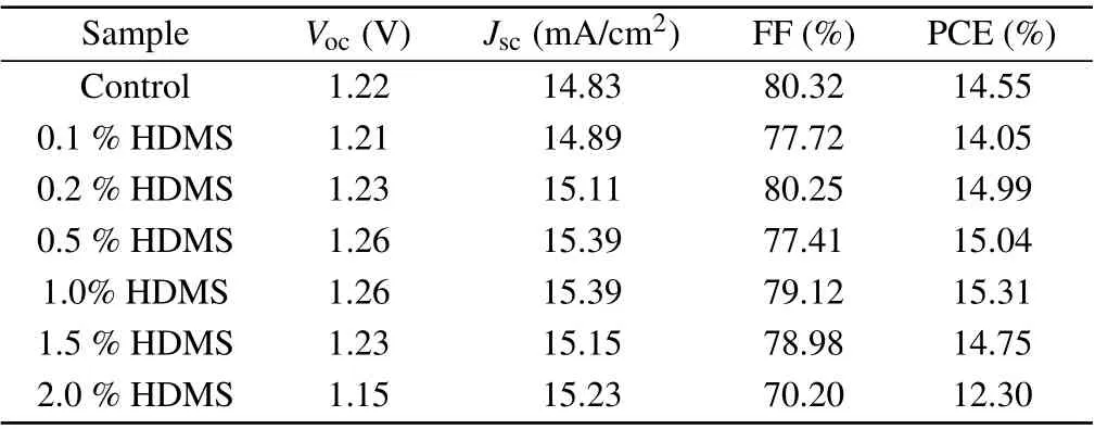
Table 1. Photovoltaic parameters of the CsPbI2Br-based devices with different concentrations of HDMS.
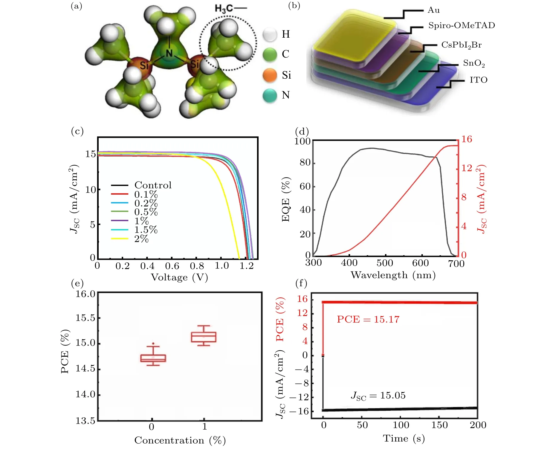
Fig.1.(a)Structure of HDMS.(b)All-inorganic perovskite device structure.(c)J–V curves of the CsPbI2Br-based devices with different concentrations of HDMS.(d)EQE curve and integrated JSC of the champion device with 1%HDMS,(e)JSC distributions for control devices(20 samples)and optimized CsPbI2Br PSCs(20 samples)with 1%HDMS,(f)the stable power output of the HDMS optimized device and long-term stability of the devices.
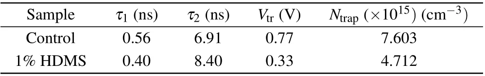
Table 2. TRPL parameters and defect state density of CsPbI2Br films with and without 1%HDMS-PbBr2.
As we all know, the performance of solar cells is related to the quality of the active layer. We also need to confirm the previous conjecture through film-related tests. Thus the perovskite films with or without HDMS were prepared. XRD was utilized to describe CsPbI2Br films after an annealing process. As shown in Fig.S2(a),both films show the same three main peaks at around 14.6°,20.8°and 29.5°,which represent the(100),(110)and(200)planes of a typical CsPbI2Br cubic phase, respectively.[22,25–27]Meanwhile, the XRD peak positions which do not vary with the adding of HDMS demonstrate that HDMS is not inside the crystal.[28]To better indicate the morphology of the control and the 1%HDMS optimized perovskite films after an annealing process, SEM images (see Fig. S2(b)) were acquired, it shows that the optimized film possesses more smooth grain boundaries compared with the control.[20,29,30]
We then move to the optical properties of the additive on the quality of the pervskite film. To investigate trap states on the surface of the control and the optimized CsPbI2Br perovskite films, photoluminescence (PL) of both was studied (Fig. 3(a)). The stronger PL intensity compared with the control film means that there are less traps on the optimized surface.[31,32]Similarly, high quality films were revealed by single carrier devices (see Fig. 2), in which the unexpected charge recombination decreased. Also, a blueshift of the PL peak from 660 nm to 648 nm can be observed, which is resulted from that high quality perovskites film as confirmed by SCLC image can effectively reduce defect density.[33]Then the TRPL decays of the two CsPbI2Br perovskite thin films with and without HDMS were investigated. TRPL decay curves(Fig.3(b))were fitted by a bi-exponential decay function,and the key parameters of the two films are listed in Table 2. The average carrier lifetime(τavg)of two kinds of films are 0.58 ns and 3.82 ns,respectively. The much longerτavgof the optimized film also agrees with the conjecture of less trap states with the help of HDMS.[33,34]only 60%. These results suggest that HDMS is an effective additive to promote the film quality and prepare high PCE and stable PSCs.Figures 4(c)and 4(d)show the water droplet contact angles of the perovskite films with or without using additive. The contact angle for the optimized one is slightly larger than the control one. The superior device stability at high humidity might come from the enhanced hydrophobicity and the improved crystal quality of CsPbI2Br films with HDMS.

Fig.2. The space-charge-limited current versus voltage of devices(a)without and(b)with 1%HDMS.
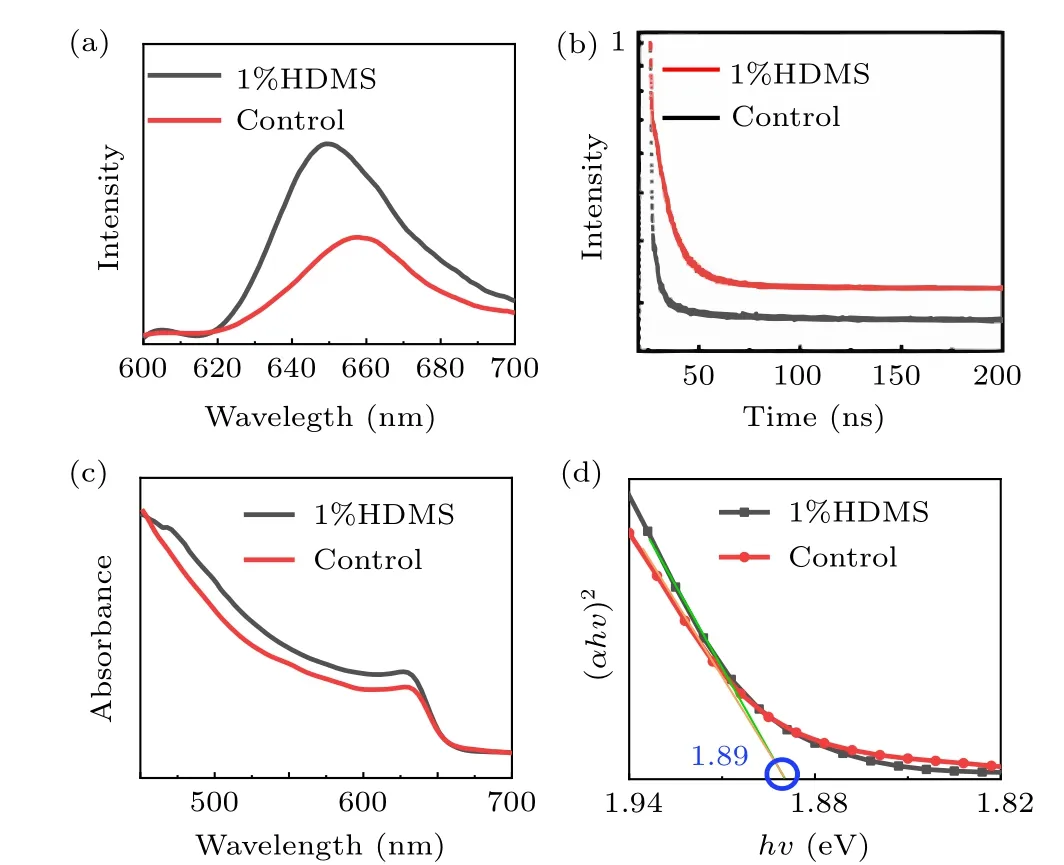
Fig.3. (a)Steady-state PL spectra,(b)TRPL curves,(c)UV–vis absorption spectra,(d) Tauc plots of CsPbI2Br films with and without 1%HDMS.
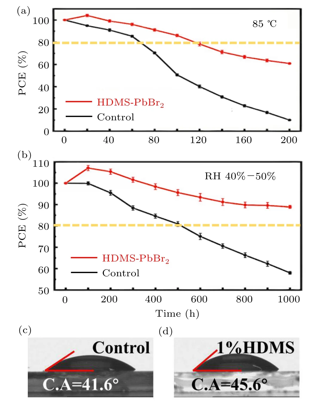
Fig. 4. Devices post stability of (a) RH 40%–50% in air and (b) 85 °C in N2. The contact angle of(c)control film(d)film with 1%HDMS.
Meanwhile,figure 3(c)shows the absorbance of the films with or without HDMS. The perovskite films with or without HDMS have almost the same absorption and the value is nearly 650 nm, which is consistent with the previous reports.[35]Using the Tauc method, the optical bandgap of these perovskite films is assessed in Fig. 3(d).[36]It is noted that a small amount of HDMS has no obvious effect on the bandgap of the CsPbI2Br perovskite film, and the values are both close to 1.89 eV, which is in line with the conclusions of other experiments. It should be noted that the HDMS film(≈510 nm)is slightly thicker than the control film(≈490 nm),which is the reason for the increased absorption strength.
Less traps promote the charge transport process,[36,37]and also enhance the stability of the perovskite devices.[38]Figure 4 demonstrates the long-term stabilities of the CsPbI2Br devices without encapsulation in the ambient atmosphere and thermal treatment, respectively. As shown in Fig. 4(a), the thermal stability of both devices at 85°C in N2indicates that the optimized ones have an enhanced tolerance to high temperatures, especially for the decay time to 80% PCEs (control device of~70 h, HDMS one of~120 h). Figure 4(b)shows the humidity stability at 25°C and RH 40%–50%.After 1000 h storing, the optimized devices with HDMS remained about 90%PCEs,while the devices without HDMS remained
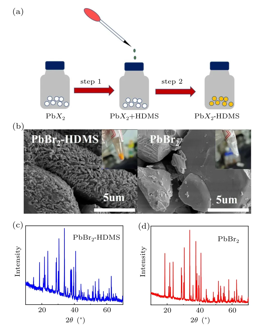
To figure out the influence of HDMS on the crystalization of perovskites, we explored a simplified experiment between HDMS and PbBr2. Interestingly,the white PbBr2powder quickly turns into yellow after adding a certain amount of HDMS, and the color does not change after purification and drying,figure 5(a)shows the whole transformation. SEM characterization was carried out to check the mouphology change. As shown in Fig. 5(b), PbBr2powder exhibits bulk blocks, while HDMS-PbBr2shows much different morphology with small plate-shaped distribution. More importantly,there are many attachments which are considered to be HDMS in the figure of HDMS-PbBr2. Then,we checked the XRD results(Figs.5(c)and 5(d)).For the two samples,the main peaks between 20°–40°do not show any different,proving that there is no change in the inherent crystal structure (PbBr2). While the new peak at below 20°in the HDMS sample might come from the coordination of HDMS with PbBr2. Based on the above experimental results, we suspect that the HDMS additive might firstly interact with PbBr2to form the HDMS–PbBr2complex,which could slow the reaction between PbBr2and CsI, resulting a higher-quality perovskite film. After the crystallization of CsPbI2Br, the HDMS might serve as a surface modification component which adheres to the surface of the perovskite grains to improve the stability.
4. Conclusion and perspectives
In summary, we demonstrate an effective additive strategy to improve the quality of all-inorganic perovskite films by adding a novel silazane additive HDMS into the perovskite precursor.The PCE of the optimized devices is enhanced from 14.55% to 15.31% with aVOCover 1.26 V due to the higher quality perovskite films with lower trap density after the incoporation of HDMS.More interestingly, the HDMS devices exhibit better humidity and thermal stability compared with the control ones. This work provides a simple and efficient strategy to enhance the device performance and stability of all-inorganic perovskite solar cells, which could fercilitate its commercialization.
Acknowledgments
This work was financially supported by the National Key Research and Development Program of China (Grant No. 2017YFA0206600), the National Natural Science Foundation of China(Grant No.21922505),and the Strategic Priority Research Program of Chinese Academy of Sciences(Grant No.XDB36000000).

- Chinese Physics B的其它文章
- A design of resonant cavity with an improved coupling-adjusting mechanism for the W-band EPR spectrometer
- Photoreflectance system based on vacuum ultraviolet laser at 177.3 nm
- Topological photonic states in gyromagnetic photonic crystals:Physics,properties,and applications
- Structure of continuous matrix product operator for transverse field Ising model: An analytic and numerical study
- Riemann–Hilbert approach and N double-pole solutions for a nonlinear Schr¨odinger-type equation
- Diffusion dynamics in branched spherical structure