
Designing current–strain-assisted superconductor–ferromagnet multi-bit memories
2022-11-21 09:30HasnainMehdiJafriJingWang王静XiaoMingShi施小明DeShanLiang梁德山andHouBingHuang黄厚兵
Chinese Physics B 2022年11期
Hasnain Mehdi Jafri Jing Wang(王静) Xiao-Ming Shi(施小明)De-Shan Liang(梁德山) and Hou-Bing Huang(黄厚兵)
1School of Materials Science&Engineering,Beijing Institute of Technology,Beijing 100081,China
2Advanced Research Institute of Multidisciplinary Science,Beijing Institute of Technology,Beijing 100081,China
Current superconducting memory devices lack the basic quality of high memory density for practical memories,mainly due to the size limitations of superconducting quantum interference devices. Here,we propose a superconductor–ferromagnet bilayer device with strain-pulse-assisted multi-bit ladder-type memory,by using strain-engineered ferromagnet domain structure to control carrier concentration in the superconductor, which is simulated by coupled Landau–Lifshitz–Gilbert and Ginzburg–Landau equations. Current-and strain-pulses are observed to deterministically control the resistivity of superconductor for one and two-bit device arrangements. The average carrier concentration of superconductor is observed to have multiple metastable states that can be controllably switched using current-pulse and strain-pulse to determine multiple resistivity states. These findings confirm the eligibility of superconductor–ferromagnet bilayers to be used as ladder-type multibit memories and open a new way for further theoretical and experimental investigations of the cryogenic memories.
Keywords: superconductor–ferromagnet bilayer, cryogenic memories, superconducting memories, vortex memories
1. Introduction
Power-efficient cryogenic memory remains one of the chanllenges in realizing fully superconducting computers.[1,2]Current single flux quantum memory is bottle-necked by its large size per cell. Although, with the active development of other types of superconducting memories, great efforts have been made to study the superconductor–ferromagnet hybrid memories.[3–5]with the scalable,low-powered high-efficiency non-volatile characteristics. Developments in magnetic tunnel junctions[6](MTJs)and cryogenic spin-valves[3,4,7–9]have attracted a great deal of attention due to their extremely low switching energy requirements (~fJ). Large unit size (low memory density) is the main disadvantage of the superconducting memories based on superconducting quantum interference devices (SQUIDs). Bits of information are stored in the form of magnetic flux quanta on SQUIDs,with advantages such as fast switching(~100 ps)and low power consumption(~120 nW/cell),[10,11]which is still far from conventional memory devices due to memory density limitations(~μm per cell). There have been reports about the reduction of Josephson junction area[12]and other types of superconductor memories, including superconductor–semiconductor hybrids,[13]Josephson magnetic random access memory,[14]Josephson transistors,[15]vortex traps with Josephson junction,[16]and the most recent anomalous Josephson junction[5](by completely avoiding superconducting loop). However, the problem of efficient cryogenic memories remains open.
The ability to transfer the magnetic state of a ferromagnet(FM) to a superconducting state makes the superconductor–ferromagnet (SF) bilayer an appealing route towards a highdensity cryogenic memory device. Therefore, an SF bilayer type device(to be used as superconducting memory)was proposed, where the FM layer controls and manipulates the superconductivity in the superconductor(SC)layer,thereby acting as a memory cell. A type-II superconductor itself lacks domain structure but it has equivalent flux quanta (vortices),which can be manipulated by magnetic domain arrangements,dynamics, and switching. In the present work, FM and SC layers are sandwiched with an insulating buffer layer in between to prohibit electrical coupling and to allow only magnetostatic coupling between the layers. The interaction between the ferromagnetic stray field and magnetization at vortices is responsible for magnetostatic coupling. Recent reports of such hybrid systems emphasize the importance of flux pinning of SC vortices by using the magnetic nano-rod array,[17]ferrite nanoparticles,[18]arrays of magnetic dots,[19]and bars,[20]magnetic templates,[21]magnetic domain walls,[22]magnetic micro-loops,[23]and more recently magnetic skyrmions.[24,25]Additionally, such a combination has also been brought forward as memristors.[26]The inverse proximity effect of SC vortices on FM domain structure has been recently investigated by Yagovstevet al.,[27]by using Usadel equations within quasi-classical Green function framework. But in the present work,this effect is observed to be significantly small(~3%–4%).
Here, a new type of cryogenic memory based on magneto-statically coupled SF bilayer(with a thin buffer layer between them)is simulated by using Landau–Lifshitz–Gilbert(LLG) equations for FM and Ginzburg–Landau (GL) equations for SC.We observe the strain-assisted ladder-type memory effect in these bilayer systems capable of performing as a multi-bit memory cell. Current- and strain-pulses are reported to deterministically control the average carrier concentration in SC.This report opens up a new way for investigating the cryogenic memory by using SF bilayer devices as memory units and provides the foundation for further theoretical and experimental investigations of long-awaited efficient cryogenic memories. This work is based on the fundamentals laid by our previous work reported in Ref.[26], and contribute to the further development of device’s working mechanism,efficiency, and control using strain pulses along with previously reported current pulses.
2. Theoretical methods
Coupled LLG equation for the FM layer and GL equation for the SC layer weresolved by utilizing in-house developed code. To determine the equilibrium domain structure,the micromagnetic simulations were used,which are based on the dynamic evolution of time-dependent LLG equation[28,29]given as follows:
wheremis the normalized magnetization given asm=M/Ms, andM=M(mx,my,mz) is the magnetization vector along three coordinate axes;γ,αm, andMsare gyromagnetic ratio,damping coefficient,and saturation magnetization,respectively;Heffis the effective field.
On the other hand, to study the magnetic structure and vortex arrangements in type-II superconductors,the GL model was used. Time-dependent GL equations were developed by Gorkov and Eliashberg,[30]and our starting point was the version of equations taken from Refs.[31–33]. Gibbs free energy of SC sample with SC order parameterψand magnetic vector potentialAis given as
where ¯his the reduced planck’s constant(i.e.h/2π),mandeare the effective mass and charge of the charge carrier,αandβare the phenomenological parameters depending on external factors,andBis the external magnetic field. Free energy can be divided into three parts,i.e.the term involving SC order parameter (superconducting energy)Hsup, the term involving magnetic vector potential(magnetic energy)Hmagand the term involving the combination of SC and magnetic order parameters(interaction energy)Hint,expressed as
whereκis the ratio of London penetration depth(λ)to coherence length (ξ). The details of the numerical formulism can be found in Section S1 of supplementary information.
The LLG equations were solved by using the spectral method, and film size of 1000 nm×1000 nm×36 nm with 5-nm grid size was simulated by using the spectral method with random initial magnetization,and the periodic boundary conditions inx–yplane,and the film was subjected to 0.5%lattice tensile strain from the substrate inx–yplane. An external tensile strain of 0.5%was added along thexaxis of the substrate strain during the strain pulse and FM domain pattern changed into an elongated maze domain structure under strain as shown in Fig.1(e). However, the finite element method was used to solve the GL equation, and the hyperfine triangular meshes were used. The film size was 600 nm×1000 nm×36 nm,and the periodicity(boundary conditions)was used along the current flow direction (i.e. xaxis). Initial conditions were set to be a fully SC sample(defined as|ψ|=1)with zero magnetic vector potential(defined asA=0)throughout the sample,The Gibb’s free energy was minimized under the influence of stray field generated by FM layer.The|ψ|2represents the superconducting charge carrier density,[34–36]which in the present work denotes the superconductivity of the Nb layer.The whole work is performed by using our developed code under the conditions described above for magnetostatically coupled LLG and GL equations. The results can be reproduced by using the above conditions and values of constants listed in Table S1 of supplementary information.
3. Results and discussion
A 600 nm×1000 nm SC layer with periodicity along thexaxis is coupled with FM layer of 1000 nm×1000 nm size with periodic boundary conditions inxyplane, and simulated with the consideration of 12-nm-thick (1ξ) insulating buffer layer between them to avoid electrical contact at a working temperature of 6 K (T/Tc=0.645). For simplicity, niobium (Nb)and nickel (Ni) are chosen to represent the SC and FM layers, the schematic diagram of the bilayer structure is shown in Fig. 1(a), and the buffer layer is not shown for simplicity. The SC layer is connected to electrodes to apply current and measure resistivity, whereas, the FM layer is exposed to strain pulses shown on the left side of Fig. 1(a). Both layers are chosen to be 36-nm thick, which corresponds to 3ξfor the SC layer and thin enough for the FM stray field to penetrate uniformly into SC, and thick enough to avoid the dominance of surface effects. Figure 1(b) shows the working flowchart of the proposed device. The current pulses reduce the average carrier concentration of the SC layer whereas strain pulses indirectly(through domain structure variation of FM layer) enhance the average carrier concentration of the SC layer. Several metastable energy states with corresponding resistivity states are observed (by combination of current and strain pulses which will be discussed in the next section)and form the basis of multibit cryogenic memories based on SF bilayer. Figure 1(c) shows the shape of the FM domain structure and position of the SC layer on the FM layer(shaded region) according to the above description. Vortices arrange themselves in the chain-like structure over the domain centers,originating from domain walls in the form of pairs(vortex and anti-vortex), and corresponding vortex structure is shown in Fig.1(d). Strained structures of FM domains and SC vortices are shown in Fig.S1 of supplementary information. The vortices are observed to appear under the FM domain wall in the form of pairs settling in neighboring domain centers behaving as an early stage drop in average carrier concentration of the SC layer along the domain wall(see Fig.S1(a)).
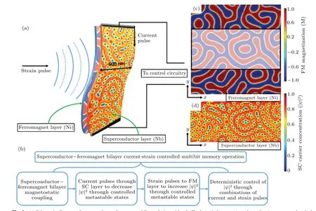
Fig. 1. (a) Schematic diagram of superconductor–ferromagnet bilayer device with a buffer layer in-between (not shown here) to prevent electrical contact,ferromagnet layer from being exposed to stress pulses. (b)Flowchart explaining the working of the proposed memory with the current assisted decrease in average carrier concentration and strain-assisted increase in average carrier concentration. (c) 1000 nm×1000 nm FM domain structure(periodic in xy plane),with the shaded region indicating the location of SC layer. (d)Corresponding SC vortex structure(periodic in x direction)over FM highlighted area describe in panel(c).
Average carrier concentration is observed to decrease successively with current pulses increasing in the superconductor and increase with successive strain pulses increasing,with several meta-stable states recorded after each current and strain pulse. Figure 2(a) shows the temporal variation of average carrier concentration and its variation with current and strain pulses. The value of average carrier concentration decreases significantly when the current pulse is applied, but after the removal of the current pulse the average carrier concentration attains a slightly lower saturation value. Here, this process is repeated for three successive current pulses, and four ladderdown types of average carrier concentration (2-bit memory)states are observed. When the current is applied, a Lorentz force is created in the vortices, which drives them in the direction perpendicular to that of current and magnetic field(in our case,BandIare perpendicular to each other), thereby pushing the vortices (and antivortices) towards the edges and giving room for the generation of new vortex anti-vortex (V–AV)pairs at domain walls. When the current pulse ends,all of these newly generated vortices (and anti-vortices) cannot annihilate each other(as they are under different domain centers,with a domain wall barrier),thereby enhancing the resistivity of the superconductor. Afterward, three strain pulses are applied to the ferromagnet,resulting in the distortion of domain structure in one direction under strain. The average carrier concentration states attained after the removal of each strain pulse have all a higher saturation value than that before the pulse,showing successive ladder-up type saturation states with strain pulses. Domain-wall motion in FM layer is faster than vortex dynamic motion,which results in the movement of domain wall from the underneath of a stable vortex arrangement.As a result, vortices and antivortices happen to find themselves in single domain center with new domain wall location.This leads to the annihilation of V–AV pairs,thereby reducing total number of vortices (and anti-vortices) in the superconductor,resulting in enhanced average carrier concentration of the sample. This effect is shown in Fig.S2 in supplementary information. Average carrier concentration is observed to increase in magnitude with each successive strain pulse applied to the SC layer. Superconductivity is observed to being enhanced successively on the application of strain pulses,as the average carrier concentration increases. Figure 2(b) displays the saturation states with current and strain pulses, showing that ladder-down states (successive states with lower average carrier concentration) and ladder-up states (successive states with higher concentration)vary with current and strain pulses,respectively. Stable states of average carrier concentration,superconducting energy, and interaction energy are shown in Fig.S3 of supplementary information.
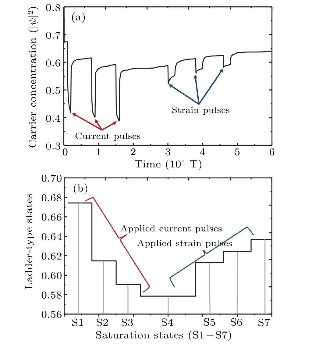
Fig.2.Temporal variation of(a)average carrier concentration(|ψ|2)and(b)ladder-type states where each step indicates a new stable state after current and strain pulses are applied to SC and FM layers, respectively. Showing multiple current–strain-controlled saturation states.
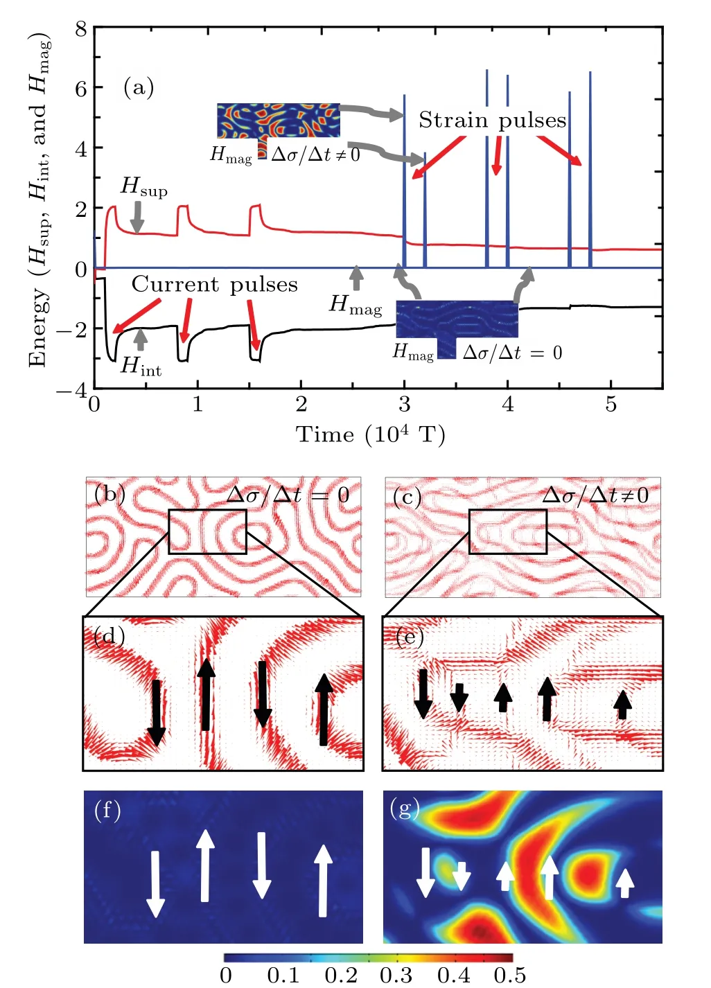
Fig. 3. Temporal distribution of Hsup, Hint, and Hmag, with insets showing spatial distribution of Hmag when strain is applied/removed (appearing as peaks in the spatial distribution of Hmag)and when strain is constant(temporally constant Hmag). Spatial distribution of current channels when (a)Δσ/Δt (strain variation) is zero and (b) Δσ/Δt /= 0, and [(c), (d)] their magnified specific regions, magnetic energy of same spatial region for (e)Δσ/Δt =0 and (f) Δσ/Δt /=0. Arrows represent the directions of current channels. Low Hmag is observed in regions bounded by opposite direction current channels compared with very high values in regions bounded by the same direction current channels.
The temporal distributions of three energy components,i.e.,Hsup,Hint, andHmagare shown in Fig. 3, with three current pulses and three strain pulses. TheHsupincreases after each current pulse, whereasHintdecreases with current pulses increasing. However, their variations are opposite to the strain pulses,i.e.,Hsupdecreases andHintincreases with strain pulses increasing. TheHmagremains unchanged after current and strain pulses, but shows a very sharp peak with Δσ(change in strain), and its spatial distributions are shown in the inset. Closed supercurrent loops have minimum energy,so the opposite neighboring current channels prefer to be in alternate directions. Owing to the rapid dynamics of domain wall in FM layer with applied/removed strain, current channels in SC formed under the domain walls are not destroyed as quickly as dynamic domain wall in the FM, resulting in additional current channels in SC under new domain wall locations of FM and forming an irregular arrangement of current channels. These irregular current channels do not follow conventional alternating directional arrangement with neighboring channels,resulting in regions with current channels in the same direction on both sides.This anomaly results in local enhancement ofHmagin the regions bounded by unidirectional current channels. Figures 3(b) and 3(c) show spatial supercurrent density plots with Δσ/Δt(strain variation) =0 and Δσ/Δt/=0,respectively. Figures 3(d)and 3(e)show their respective highlighted regions to understand the local variation ofHmag, where arrows indicate the local supercurrent directions, where figures 3(f) and 3(g) show corresponding localHmagdistribution. It can be seen clearly that the region bound by oppositely directional supercurrent possesses a lower value ofHmag,whereas the region bound by supercurrent in the same direction has an much higher values ofHmag.
To have a better understanding of the phenomenon, the spatial distribution of carrier concentration, superconducting energy, interaction energy, and phase of the order parameterψbefore, during, and after the current pulse, and during and after strain pulses are all shown in Fig. 4. Figure 4(a) shows the chain-like vortex distribution before the current pulse is applied, which changes to a lower value of average carrier concentration (Fig. 4(b)) during the current pulse and attains a lower average carrier concentration state (Fig. 4(c)) of the same shape as that before the application of the current pulse.Whereas figure 4(d) shows vortices during the strain pulse,which, when being removed, come back to the state shown in Fig. 4(e). Figures 4(f)–4(i) show the spatial distributions of superconducting energy which increases from the initial value (Fig. 4(f)) to a higher value (Fig. 4(g)) when current is applied. The superconducting energy has a higher saturated energy state when the current is removed. Comparing Fig. 4(h) with Fig. 4(j), superconducting energy is observed to decrease after the application of the strain pulse(which can be observed qualitatively from the shade change in the diagram). Figures 4(k)–4(o) show the interaction energy attains a lower value after the application of the current pulse (i.e.Figs. 4(k)–4(m)), and increases when the strain pulse is applied(Figs.4(m)–4(o)).Figures 3(p)–3(t)represent the phases of the complex order parameterψ, which in principle indicate vortex dynamic path,and it can be observed that initially vortices appear at the domain wall centers and attain a static position (Fig. 4(p)). But they are hugely dynamic due to additional Lorentz force when the current is applied(Fig.4(q)),which then decreases after the current is removed. Furthermore, it is observed that strain does not significantly change vortex dynamics(Fig.4(s)).
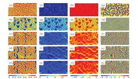
Fig. 4. Spatial distribution of [(a)–(e)] carrier concentration (|ψ|2), [(f)–(j)] superconducting energy (Hsup), [(k)–(o)] interaction energy (Hint), and[(p)–(t)]phase of complex order parameter ψ,whereas,five stages corresponding to(i)before(ii)during,and(iii)after the current is used in SC layer and(iv)during and(v)after the strain is applied in FM layer.
Extended alternating current–strain cycles each show a very predictable control over the superconductivity in the SC layer as shown in Fig.5(a),which also shows an enhancement in data redundancy as writing-erasing cycles are repeated and discrete logic 0 and 1 are observed. These current and strain pulses can be applied in any combination to bring SC average carrier concentration to any desired state,making this type of device a strong candidate for multibit ladder-type cryogenic memories. Several possible sources of strain pulses (ultrasonic,seismic,piezo-electric,etc.) can be used during device fabrication. A design of 2×2 array is shown in Fig.5(b). Resistivity can be measured(readout)by several well-known industrial techniques,for example,simple current/voltage measurements (small enough to disturb the vortex arrangement)across the sample. In short, the observed resistivity states in the superconductor in SF bilayer and its current and strain pulse assisted deterministic control over multiple metastable resistivity states make this type of device a strong candidate for high density multibit cryogenic memories. This research opens a new way for theoretical and experimental study of the usage of such devices as superconductor memory.
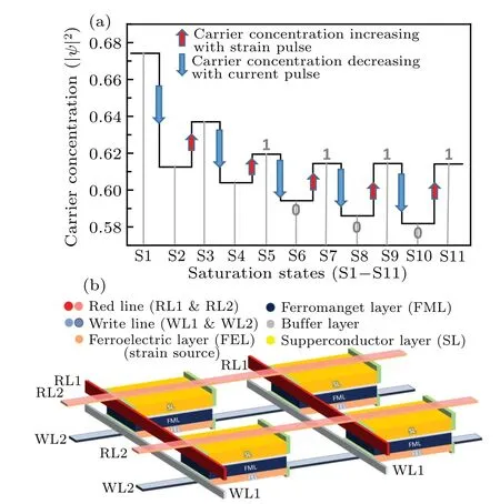
Fig. 5. (a) Temporal variation in average carrier concertation of the superconductor with current pulse and strain pulse under extended alternating states, showing enhancement in data redundancy with usage. Logic 0 and logic 1 are also shown for reference. (b)Design of 2×2 memory array of the proposed device(nonscaled).
Though the proposed device embodies a new idea and a new type of memory unit,it is still far from replacing the existing memory device.Fast switching time,highly precise vortex/domain control,ability to address a large number of memory cells and memory density comparable to current semiconductor or ferroelectric memories are some of the required characteristics for the existing device to be used in practical applications. An extensive theoretical and experimental research is required to analyze the feasibility of the presented device for practical use.
4. Conclusions
In short, we proposed a superconductor–ferromagnet bilayer type of memory device with current–strain coupled deterministic control of superconductivity. Precise control of superconductivity makes the proposed bilayer device an efficient multibit memory cell. Disturbance of vortices’ arrangement over the domain centers by applying strain makes the multiple metastable states of average carrier concentration (i.e.superconductivity) observable. Average carrier concentration decreases with current pulses increasing due to high vortex dynamics, whereas this effect is observed to be absent in strain pulses,leading to an increase in average carrier concentration.The precisely predicted states are observed after several readwrite cycles,due to stabilization of energy states in the device.We present this type of device as a new candidate for cryogenic memory and provide a new device for further theoretical and experimental research.
Acknowledgements
Project sponsored by the National Natural Science Foundation of China (Grant Nos. 52150410420 and 51972028)and the National Key Research and Development Program of China(Grant No.2019YFA0307900).
猜你喜欢
Chinese Physics B(2022年10期)2022-10-26
客联(2021年9期)2021-11-07
青年生活(2019年16期)2019-10-21
思维与智慧·上半月(2019年2期)2019-03-08
文学港(2017年11期)2017-12-06
商情(2017年17期)2017-06-10
高中生学习·高一版(2017年4期)2017-04-14
星火·中短篇小说(2017年2期)2017-03-20
现代家庭(2016年6期)2016-06-14

- Chinese Physics B的其它文章
- A design of resonant cavity with an improved coupling-adjusting mechanism for the W-band EPR spectrometer
- Photoreflectance system based on vacuum ultraviolet laser at 177.3 nm
- Topological photonic states in gyromagnetic photonic crystals:Physics,properties,and applications
- Structure of continuous matrix product operator for transverse field Ising model: An analytic and numerical study
- Riemann–Hilbert approach and N double-pole solutions for a nonlinear Schr¨odinger-type equation
- Diffusion dynamics in branched spherical structure