
Resistive switching properties of SnO2 nanowires fabricated by chemical vapor deposition
2023-10-11 07:56YaQiChen陈亚琦ZhengHuaTang唐政华ChunZhiJiang蒋纯志andDeGaoXu徐徳高
Chinese Physics B 2023年9期
Ya-Qi Chen(陈亚琦), Zheng-Hua Tang(唐政华), Chun-Zhi Jiang(蒋纯志), and De-Gao Xu(徐徳高)
1School of Physics,Electronics and Electrical Engineering,Xiangnan University,Chenzhou 423000,China
2Key Laboratory of Low Dimensional Quantum Structures and Quantum Control,School of Physics and Electronics,Hunan Normal University,Changsha 410006,China
Keywords: Au/SnO2 NW/Au device,resistive switching characteristics,resistive switching mechanism
1.Introduction
Owing to its simple structure, high storage density and low power consumption, the RS effect-based resistive random access memory (RRAM) is considered to be an ideal choice for the next generation of non-volatile memory.[1,2]In recent years, many kinds of materials have been developed for the design of RRAM, such as metal oxide,[3]sulfide,[4]and graphene.[5]Among them, tin dioxide (SnO2) is one of the most promising materials because of its compatibility with complementary metal oxide semiconductors and unique electrical performance.[6,7]
Recently, the RS characteristics of SnO2nanostructures have been reported in the literature, including both unipolar resistive switching[8–10]and bipolar resistive switching.[11–13]For instance, Liuet al.[14]constructed Cu/SnO2nanorod arrays: ZnO(NP)/FTO bipolar resistive switching devices, and speculated that the RS effect is caused by the formation and fracture of Cu2+conducting filaments under the action of an electric field.Yang and Lu[15]deemed that the Joule heating is the main cause of filament formation and rupture in unipolar resistive switching devices.Neihet al.[16]fabricated a rutile-structured SnO2NW resistive memory which shows a significantIon/Ioffratio(about 1000),and the various resistive switching phenomena were well explained by the change of the Schottky barrier height at the interface of SnO2/Au.Although researchers have proposed relevant models to explain various RS behaviors,there is no consensus on the role of interface contact,ion motion,Joule heating effect and other factors in the resistance mechanism.[17–20]Therefore, there are still a lot of work to be done to promote the application of RS devices.Moreover, a more in dept understanding of the oxide resistance mechanism will also advance the development of artificial intelligence.[21,22]
In this work, we first construct an Au/single SnO2NW/Au two-terminal nanodevice based on SnO2NWs synthesized by chemical vapor deposition,then investigate the RS characteristics in air and vacuum.We find that the devices exhibit non-volatile resistive memory characteristics.According to the double Schottky emission model and the Fowler–Nordheim(FN)tunneling effect mechanism,we further clarify the RS mechanism from the perspective of Joule thermal effect and the movement of oxygen ions under the electric field.
2.Experimental methods
The SnO2NWs[23]prepared by chemical vapor deposition were placed in an alcohol solution for ultrasonic dispersion and then dropped on a heavily doped N-type silicon wafer with 100-nm-thick oxide layer.Au electrodes with a thickness of 100 nm were deposited on both ends of SnO2NWs by photolithography process, coating technology, and chemical lift-off to construct a two-terminal Au/single SnO2NW/Au device.Then the nanodevice was placed in a horizontal hightemperature furnace which had been evacuated, and a carrier gas(50 sccm of argon+50 sccm of hydrogen)was introduced,and the annealing temperature was set to 150°C for 1 h.
The morphologies of the materials were characterized by a scanning electron microscope (SEM, FEI, NovaSEM-450),and the crystal structure was determined by x-ray diffraction(XRD)(Aolong Y2000,CuKα,λ=0.15405 nm).In Fig.1,the thickness of the prepared nanowires is relatively uniform,and the length can reach several tens of micrometers.All peak positions in the XRD pattern are consistent with the standard peaks of SnO2in bulk material (card number 41-1445), indicating that the SnO2NWs have a tetragonal rutile structure.Electrical transport measurements were executed on a probe station at room temperature by using a Keithley SourceMeter 2602.The probe was placed in a homemade vacuum chamber,which can be vacuumed to a base pressure of less than 10-1Pa by a mechanical pump.

Fig.1.(a) SEM image of SnO2 NWs with insert showing XRD image of SnO2 nanowires.(b)SEM image of Au/SnO2 NW/Au device.
3.Results and discussion
3.1.Resistive switching characteristics
The Au/SnO2NW/Au device is placed in a high vacuum environment.In order to avoid the influence of oxygen molecules initially adsorbed in air,we repeatedly apply a bais of 5 V to the device until itsI–Vcurve is stabled.In Fig.2.We can see that theI–Vcurve near 0 V exhibits an obvious nonlinear characteristic,which suggests that the Schottky contact is formed between SnO2NW and Au electrode.[24]Subsequently,a bias voltage of 10 V is applied to the device,then the device is in a high resistance state(HRS)under a low bias voltage.When the applied voltage increases to the set voltage of the device, the output current suddenly rises at a voltage of about 5 V(-5 V),and correspondingly,the resistance switches from HRS to low resistance state(LRS).

Fig.2.The I–V curves of Au/SnO2 NW/Au device under different bias voltages, with left-hand insert showing magnified part of I–V curve between-5 V and 5 V, and right-hand insert indicating I–V curve and its theoretical fitting curve.
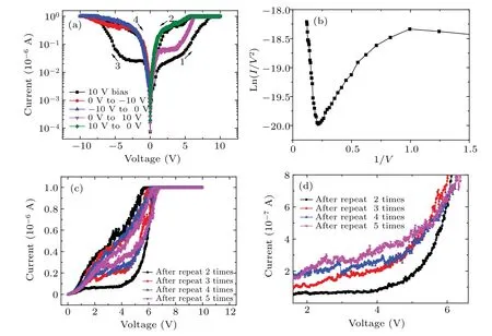
Fig.3.(a)The I–V curves of Au/SnO2 NW/Au device under different scanning sequences,(b)fitting curve of conductance mechanism in 1 process of panel(a).(c)Positive voltage I–V curve after different scanning times at negative voltage scans,(d)magnified parts between 2 V and 4 V in panel(c).
Notably, in oeder to prevent the device from being damaged due to excessive current, a limiting current of 1 μA is used to protect the device in the experiment.As shown in Fig.3(a),theI–Vcurve shows an obvious hysteresis loop effect with counterclockwise circulation in the forward direction and backward direction.After that, the bias sweep at a negative bias is applied from 0 V to-10 V,the device maintained a high current and LRS,which indicates that the device has obvious non-volatile storage characteristics.In fact, the device keeps LRS (HRS) in the low bias region while maintaining the the direction of original electric field after a power failue of about 2 days.When a reverse bias voltage of 10 V is applied to the device, HRS appears first, and the current is low.Then the device resistance switches from HRS to LRS while the sweep voltage gradually increases to about 5 V,suggesting that the transition between high resistance state and low resistance state can be achieved by applying a large reverse bias.After that, when the bias voltage sweeps back from 10 V to 0 V,the device always maintains a low resistance state.In addition,theIon/Ioffratio is about 20 at the read voltage of 3.1 V.
Figure 3(c) shows the positive voltageI–Vcurve after negative voltage scanning for different scanning times.The scanning sequence of negative bias is 0 V→-10 V→0 V.With the increase of negative bias scanning times,the current flowing through the device under low forward bias increases obviously, and the hysteresis loop effect weakens.In the range of 2 V–4 V, the device current rises very slowly as the applied bias voltage increases, as illustrated in Fig.3(d).Figure 4 shows theI–Vcurves of the device under the sequential bias voltage of 0 V→-5 V→0 V→5 V→0 V after being placed in air for a period of time.At low bias voltage,the current flowing through the device is about pA level and it rises sharply with the increase of the bias voltage,reaching the limit current at about-3.8 V(3.2 V).Moreover,theI–Vcurve always shows an obvious counterclockwise hysteresis loop effect even if the measurement is repeated 8 times.The current measured the 8th time is significantly less than that measured the first time.Subsequently,we find that the device still maintains a high current and low resistance state when a sequential bias voltage of 0 V→5 V→0 V is applied,indicating that the device possesses distinct non-volatile memory characteristics in air.When the bias voltage of 0 V→-5 V→0 V is applied, the device first shows a low current and high resistance state,and then switches from HRS to LRS around-4 V,which indicates that the applied voltage required for the transition between HRS and LRS is reduced after the electric field adjustment (as shown in Fig.5(b)).And theIon/Ioffratio of the device is about 104by using a read voltage of-1 V.As the number of scans increases, the resistance state of the device shows an upward trend.Furthermore, theIon/Ioffratio of the device is reduced to 103after repeating 8 times at 5-V cyclic sweeping bias voltage(as shown in Fig.5(a)).

Fig.4.Cyclic I–V curves of Au/SnO2 NW/Au device after being exposed to air for a period of time, with left-hand insert showing I–V curves in the range of 0 V to-1 V for the first cycle and its theoretical fitting curve, and right-hand insert indicating fitting curve of conductance mechanism in 1st process for the first cycle.

Fig.5.(a)Stability test of Au/SnO2 NW/Au device in air,and(b)I–V curves of the device under different scanning sequences.
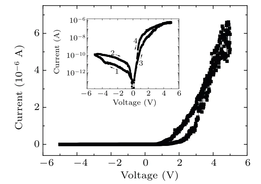
Fig.6.The I–V curves of Au/SnO2 NW/Au device recorded after repeatedly scanning positive bias voltage scans (0 V→10 V→0 V) ten times,with left-hand insert showing the logarithmic plot of I–V.
When a bias voltage of 0 V→10 V→0 V is repeatedly applied to the device 10 times,it exhibits obvious rectification characteristics,and the rectification switch ratio can reach 104,as shown in Fig.6.Meanwhile, the hysteresis loop effect of the device is significantly weakened.
3.2.Resistive switching mechanism
For discussion, the SnO2NW in the device can be divided into three parts,as shown in Fig.2.Evidently,under the conditions of no bias or low bias,the oxygen defects are uniformly distributed in the SnO2NW after the Au/SnO2NW/Au device has been hydrotreated.When a high electric field in the MV/m range is applied, these defects act as solid electrolyte for oxygen ion migration.[25]The Au/SnO2NW/Au device is equivalent to two back-to-back Schottky diodes[26](Fig.7(a)).Whether the device is forward biased or reverse biased, one of the two back-to-back Schottky diodes is always forward biased and the other is reverse biased, and the current flowing through the device depends on the reverse-biased diode current.We denote the height of the double Schottky barriers at the Au/SnO2interface byΦBn,and the applied bias voltage of the device byV.Considering the influence of defect and image force on the Schottky barrier height, the total current flowing through the device can be deduced and expressed as[27,28]
whereA*is the effective Richardson constant,Sthe crosssectional area,Tthe temperature,kthe Boltzmann constant,ethe electron charge,andnthe ideality factor.
TheI–Vcurve of 0 V→1 V under 5-V bias voltage in vacuum can be fitted by Eq.(1), as shown in the lower right insert of Fig.2.WhenA*takes 120 A/cm2·K2,[29]the Schottky barrier height at the Au/SnO2interface is 0.47 eV, which is very close to the result previously reported.[30]The ideality factornis 1.17 that is within a reasonable range.[27]
The stage curve before and after current mutation at a bias voltage of 10 V can be fitted by Fowler–Nordheim (FN)tunneling mechanism,as shown in Fig.3(b).The voltage drop is mainly concentrated on the reverse biased Schottky junction when the device is in HRS before current mutation.[31]After the device is transformed from HRS to LRS, the relationship between ln(I/v2)andv-1is a linear,indicating that when the external bias voltage is greater than 5 V,the FN tunneling currents will dominate.[32,33]Subsequently, as the applied bias voltage increases, the ratio of the voltage on the reverse biased Schottky junction to the applied bias voltage decreases.Accordingly, the ratio of the voltage on the a–b segment of the SnO2NW increases, so the oxygen ions in the a–b area can move to the anode (a-point) under the action of external electric field, and the height and width of the left Schottky barrier increase slightly[16,31](Fig.7(b)).Meanwhile,the oxygen vacancy concentration near the right Schottky junction(bpoint)increases,and the height and width of the right Schottky barrier decrease slightly.At this time, the Au/SnO2NW/Au device is equivalent to two different back-to-back Schottky diodes(in the right inset of Fig.7(b)).The variation of Schottky barrier caused by the movement of oxygen ions can also lead to A–B phenomenon of theI–Vcurve in Fig.2.Changing the direction of the electric field,the right Schottky diode is forward-biased and the other is reverse-biased,the device is in the HRS under low bias region.The oxygen ions migrate to the b-point as the applied electric field intensity increases to the threshold value,which reduces the height and width of the left Schottky barrier,then it is converted from HRS to LRS(Fig.7(c)).Keeping the original direction of electric field,the device maintains the LRS and exhibits obvious non-transitory storage characteristics.
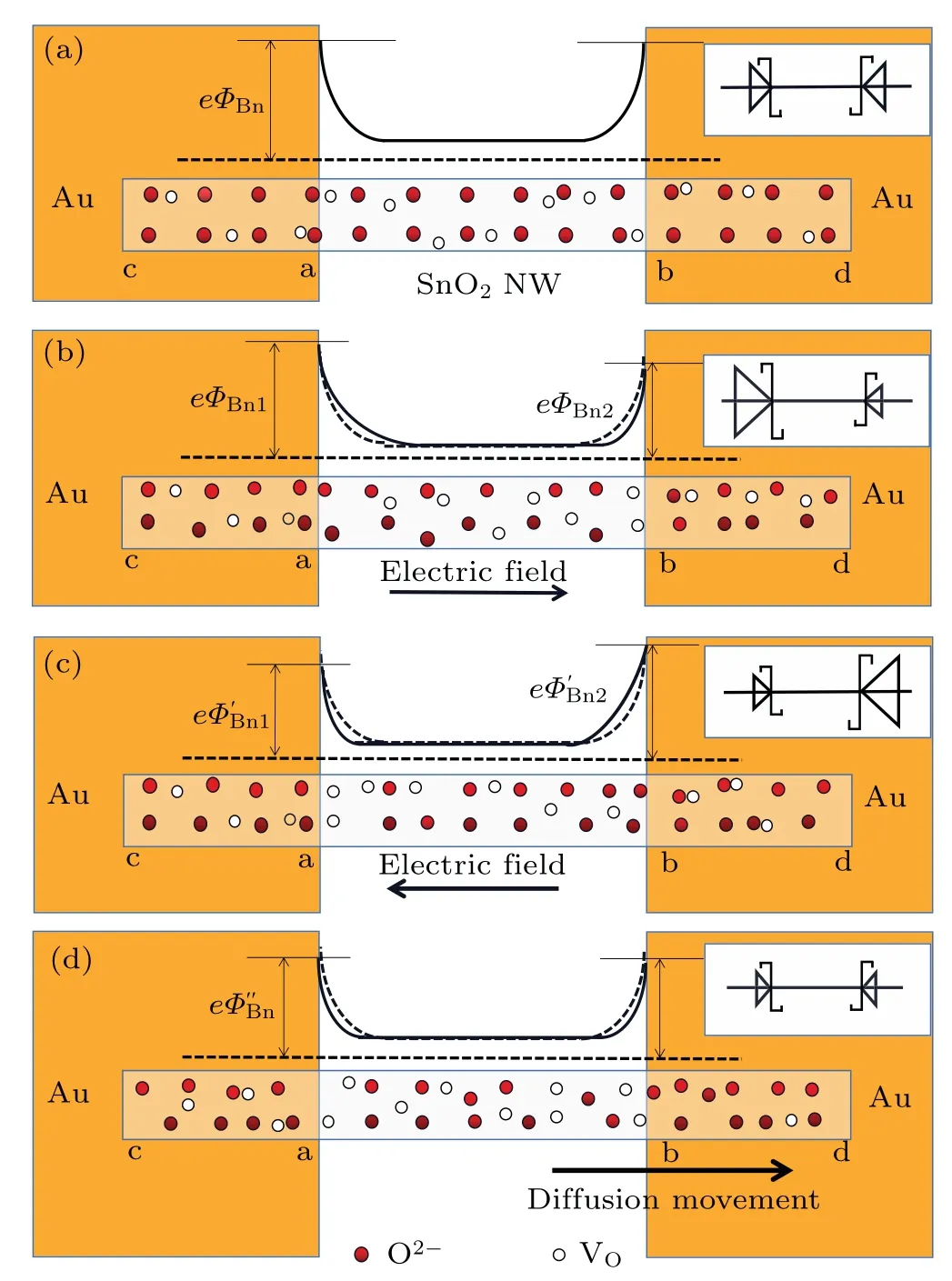
Fig.7.Schematic diagram of resistance switching mechanism in Au/SnO2 NW/Au device, with Schottky diode size reflecting the change of Schottky barrier height and width.The larger Schottky diode is accompanied by higher and wider Schottky barriers.
In general, a nanosystem will generate joule heat when current flows through it.In this case, the carriers obtaining more energy to pass through the reverse-biased junction barrier can form a larger current, just as shown in the C–D segment ofI–Vcurve in the upper left-hand inset of Figs.2 and 3(c).When the applied voltage is further raised, the built-in potential difference of the reverse-biased junction also increases,[28]and it becomes more difficult for carriers to cross the reverse-biased junction barrier,so we find that the current flowing through the device increases very slowly, or even remains unchanged in the range of 2 V–4 V.
Moreover, when the device is repeatedly scanned with 0 V→-10 V→0 V bias voltage, the oxygen ions continue to migrate to the anode(b-point),so the oxygen-ionic concentration in the a–b segment near the b-point is higher than that in the b–d part.Meantime, the continuous flow of current in the a–b segment generates a large amount of Joule heat,which makes the temperature of a–b segment higher than that of a–c and b–d parts.Then the oxygen ions in the a–b segment diffuse into the b–d area.[34]Hence the b–d segment is equivalent to the storage area of oxygen vacancies in the nanodevice.After a period of diffusion,the concentration of oxygen vacancies in the a–b area will increase significantly,which reduces the width and height of two back-to-back Schottky barriers, as represented in Fig.7(d).However, the Schottky barrier height extracted by fitting with the double Schottky model is about 0.84 eV, which may be caused by the adsorption of oxygen molecules in air and the state of the semiconductor surface.[27,35]
In addition,the ideal factornof the fitting parameter deviates far from 1, indicating that the carrier transport mechanism deviates greatly from the thermal emission model, and the main reason may be the existence of tunneling current in high oxygen defect semiconductor.[36,37]For the lower righthand insert in Fig.4, linear relationships of ln(I/v2) andv-1are obtained in the LRS region, suggesting that it is a typical FN tunneling mechanism.And initial voltage of the FN tunneling effect becomes smaller after electric field regulation has been implemented,which is explained by the previous conclusion that the width of the two back-to-back Schottky barriers is narrowed due to the diffusion of oxygen ions.It is also for this reason that the current flowing through the device is 100 times higher than that in the original vacuum under the same bias voltage in air.Meantime,the equivalent resistance of the reverse-biased Schottky junction decreases obviously, so that the voltage drop of the a–b segment of the nanowire is significantly increased,and the oxygen ions migrate under the action of a relatively small electric field.The schematic diagrams of the potential barrier are similar to Figs.7(b)and 7(c).Hence when the operating voltage of the device decreases from 3.1 V to-1 V,theIon/Ioffratio is increased by 500 times.
When a bias voltage of 0 V→10 V→0 V is repeatedly applied 10 times in air, the oxygen ions continue to accumulate towards the high potential electrode(a-point).Then the height and width of the left Schottky barrier increase significantly.When the direction of the electric field is changed, the device exhibits obvious rectification characteristics.Meanwhile,owing to the injection of carriers, the adsorption of oxygen molecules is enhanced in air, and the concentration of oxygen vacancies in the SnO2NW is reduced, which makes the regulation of the movement of oxygen ions weakened under 5 V bias, and the hysteresis loop effect is reduced (Fig.6).According to the comprehensive analysis of double Schottky emission model and FN tunneling effect, we find that the RS behaviors of the device are mainly related to the migration of oxygen ions under applied electric field.Moreover, the RS performance can be improved by the diffusion of oxygen ions caused by Joule heating effect which is produced by repeatedly applying large bias voltage to the device.
4.Conclusions
In summary,we investigated the RS characteristics of hydrogenated Au/SnO2NW/Au nanodevices under the action of electric field.The results reveal that when the operating voltage of the device decreases from 3.1 V to-1 V, the resistive switch increases from 20 to 104.According to the double Schottky emission model and the FN tunneling effect mechanism, we conclude that when the external electric field increases, the oxygen ions in the SnO2NW move toward high potential area, changing the height and width of the reversebiased Schottky barrier.When a strong electric field in the same direction is continuously applied to the device,the oxygen ions of a–b region diffuse to the b–d region.In this way,most of the oxygen vacancies are localized at the middle effective length.An increase of oxygen vacancy concentration in the middle part of SnO2NW improves the resistanceswitching performance.Our research results show that the excellent resistive switching memory performance can be obtained by modulating the movement of oxygen ions in SnO2NWs with certain oxygen defects by external electric field,which provides a new idea for designing high-performance resistive switching devices.
Acknowledgements
The authors thank Prof.Gang Ouyang for stimulating discussion and also thank Prof.Dongsheng Tang for his help in experiment.
Project supported by Chenzhou Science and Technology Plan Project of China (Grant No.ZDYF2020159) and Scientific Research Project of Hunan Provincial Department of Education(Grant No.21C0708).

- Chinese Physics B的其它文章
- Dynamic responses of an energy harvesting system based on piezoelectric and electromagnetic mechanisms under colored noise
- Intervention against information diffusion in static and temporal coupling networks
- Turing pattern selection for a plant–wrack model with cross-diffusion
- Quantum correlation enhanced bound of the information exclusion principle
- Floquet dynamical quantum phase transitions in transverse XY spin chains under periodic kickings
- Generalized uncertainty principle from long-range kernel effects:The case of the Hawking black hole temperature