
Ultra-high photoresponsive photodetector based on ReS2/SnS2 heterostructure
2023-10-11 07:56BinghuiWang王冰辉YanhuiXing邢艳辉ShengyuanDong董晟园JiahaoLi李嘉豪JunHan韩军HuayaoTu涂华垚TingLei雷挺WenxinHe贺雯馨BaoshunZhang张宝顺andZhongmingZeng曾中明
Chinese Physics B 2023年9期
关键词:韩军
Binghui Wang(王冰辉), Yanhui Xing(邢艳辉), Shengyuan Dong(董晟园), Jiahao Li(李嘉豪),Jun Han(韩军), Huayao Tu(涂华垚), Ting Lei(雷挺), Wenxin He(贺雯馨),Baoshun Zhang(张宝顺), and Zhongming Zeng(曾中明),‡
1Key Laboratory of Opto-electronics Technology,Ministry of Education,College of Microelectronics,Beijing University of Technology,Beijing 100124,China
2Nanofabrication Facility,Suzhou Institute of Nano-Tech and Nano-Bionics,Chinese Academy of Sciences,Suzhou 215123,China
Keywords: two-dimensional material,ReS2,heterostructure,photodetector
1.Introduction
Transition metal dichalcogenides(TMDs)with the chemical formulaMX2(X=S, Se, Te andM=transition metal)are widely used in various fields due to their weak interlayer coupling, good optical transparency, and large bandgap,[1–3]such as gas sensors,[1]photodetectors,[4]inverters, and solar cells.Most of the previous researches on TMDs have focused on the Mo and W families, which summarized the material growth and device preparation of photodiodes and rectifiers.[5–9]However, the recently discovered ReS2possesses properties quite different from MoS2, which has aroused extensive researches.[10,11]First,due to the twisted 1T crystal structure of ReS2,it has a direct bandgap independent of thickness,[12,13]which makes the optical properties of bulk ReS2and single-layer ReS2similar,provides a good basis for mechanical exfoliation.In addition, ReS2has an ultra-high light absorption rate.It has been reported in the literature that the responsivity of multilayer ReS2photodetectors can reach 88600 A/W.[14]However,one of the most serious problems of ReS2photodetectors is the slow response speed,which reaches hundreds of seconds.[15]In order to solve this problem, researchers have adopted heterostructures.Two-dimensional heterojunctions materials are combined by van der Waals forces and not affected by lattice mismatch,and different materials can be freely matched, and the detectors with heterojunctions can exhibit various interesting properties.[15,16]For example, the ReS2/graphene/WSe2heterojunction photodetector prepared by Wanget al.has a response speed of 44 ms under 532-nm light.[17]The ReS2/ReSe2heterojunction photodetector prepared by Choet al.has a similar response time of 0.4 s under 400-nm and 550-nm light.[12]Although the response speed of the devices was been greatly improved, it is at the expense of the responsivity.The device responsivity of Wanget al.[17]is 430 mA/W,and that of Choet al.[12]is only 21.07 mA/W.
In this paper, it is reported that the photodetector based on ReS2has ultra-high responsivity and response speed in seconds.We chose SnS2material as the light absorbing layer,and prepared a vertical structure ReS2/SnS2heterojunction photodetector.The detector has a responsivity of 4706 A/W under 365-nm light,which is higher than the previously reported detectors based on ReS2heterojunction,[15,18]and the response speed of the detector is only 1.4 seconds.In addition,our detector also had a high detectivity of 5.29×10¹²Jones and an ultra-high external quantum efficiency(EQE)of 1.602×10⁶%.The study paved the way for improving responsivity and reducing response time of the ReS2-based heterostructures photodetector.
2.Experimental details
2.1.Device fabrication
The ReS2/SnS2heterostructure device was fabricated on the SiO2/Si substrate using a dry transfer technique.The fewlayer flakes of ReS2and SnS2were mechanically exfoliated from commercially bulk crystal.First, the thin ReS2flakes were exfoliated on a highly p-doped Si substrate with a 300-nm-thick SiO2layer.Then,the same method was adopted for transferring several layers SnS2onto the ReS2under the optical microscope assisted by aligned transfer system.Finally,to fabricate the heterostructure device, the electrode patterns were produced by electron–beam lithography system (EBL,Raith eLINE Plus)and Ti/Au(10 nm/50 nm)metals were deposited by electron–beam evaporation (Ulvac Ei-5z) to form source and drain electrodes.
2.2.Result and discussion
Figure 1(a) shows the schematic diagram of the ReS2/SnS2heterojunction device.The mechanical exfoliation ReS2and SnS2were transferred to an SiO2/Si substrate sequentially.The electrodes are placed on the ReS2.In order to obtain the interface information of ReS2and SnS2layer of the device, the high-resolution transmission electron microscope (HRTEM) was used, as shown in Fig.1(b).The interfaces between SnS2and ReS2, ReS2and substrate are clear and flat.Figure 1(c) shows the energy dispersive x-ray spectroscopy (EDS) of the device.The distribution of each layer element was uniform, and these elements are corresponding to each layer material of HRTEM,indicating that no diffusion and impurity element were introduced in the process of device preparation.The thickness of ReS2(8 nm)and SnS2(14 nm)is shown by atomic force microscopy(AFM)in Fig.1(d),and the inset is the surface topography image of the heterojunction.Figure 1(e)is the Raman spectrum of the single ReS2and SnS2material and the ReS2/SnS2heterojunction.SnS2(the blue line)has a main peak A1gat 313.4 cm-1,which is consistent with the literature report.[19]Typical Raman characteristic peaks of ReS2(the red line) are also observed at 154 cm-1(E2g) and 215 cm-1(A1g).[20]The black line in Fig.1(e)shows the characteristic peaks of the ReS2/SnS2heterojunction.The above peaks are observed in overlapping areas, indicating the good quality of the heterojunction.Figure 1(f)is the scanning electron microscope image of the device after the preparation of the electrodes.The light absorption layer SnS2and the transmission layer ReS2could be clearly observed,and the electrodes are only connected on the ReS2,and the device is regular in shape and a clean surface.The above results show the good structure and successful fabrication of the ReS2/SnS2heterojunction device.

Fig.1.Characterization of ReS2/SnS2 heterostructure.(a)Schematic diagram of the ReS2/SnS2 heterostructure.(b)HRTEM image.Scale bar:10 μm.(c)EDS of the corresponding elements of the photodetector.(d)Height profiles of corresponding ReS2 and SnS2 flakes in AFM.The inset shows a topographic AFM image of the ReS2/SnS2 device.(e)Raman spectrum of the isolated ReS2,isolated SnS2,and their overlapped regions.(f)The SEM image of the heterostructure,where the scale bar is 5 μm.
The transport properties of the device under dark conditions were measured.Figure 2(a)shows the relationship of the source–drain current (Ids) and the source–drain voltage (Vds)when the gate voltage (Vg) varies from-80 V to 80 V.TheIds–Vdscurves are straight lines passing through the origin,indicating that ReS2forms a good ohmic contact with Ti/Au.AsVgincreases, the current increases accordingly, meaning that the device has obvious gate voltage control characteristic.Figure 2(b) shows theIds–Vgrelationship of the device whenVdschanges from-3 V to 3 V.WhenVgbelow-30 V(Vth),Idsapproaches 0 A,and whenVgover-30 V,Idsrises gradually.When theVgis negative, the direction of the external electric field is opposite to that of the built-in electric field.WhenVg<Vth(-30 V),the external electric field plays a major role,electrons flow from ReS2to SnS2and the carrier concentration decreased,resulting in the current approaches 0 A,whenVg>Vth(-30 V), the direction of the electric field pointed from ReS2to SnS2,and electrons entered ReS2under the action of the electric field, increasing the carrier concentration in the channel, thereby increasing the drain current.The device also switched from the insulating state to the conducting state,showing obvious n-type conductivity.Figure 2(c)shows the logarithmic curves ofIdsversusVg,which characterizes the on-off ratio of the device.The on-off ratio reaches 104, indicating that the device has a high current regulation capability.

Fig.2.The I–V characteristics of the device based on ReS2/SnS2 heterostructure under non-illumination condition.(a) Ids–Vds output characteristics under various back gate voltages.(b) Ids–Vg transfer curves at various drain voltages.(c) The logarithmic curves of the transfer characteristic curves of the ReS2/SnS2 heterojunction.
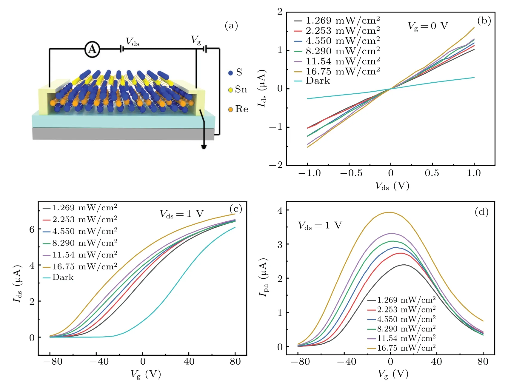
Fig.3.(a)Schematic diagram of the device measure setup.(b)Output characteristic curves under different incident power densities(Vg=0 V).(c)Transfer characteristic curves of the device under different incident power densities(Vds =1 V).(d)Photocurrent(Iph)as a function of Vg under different incident power densities(Vds=1 V).
The optoelectrical properties of the device were tested under 365-nm light source.Figure 3(a) is a schematic diagram of the measurement setup,in which the gate voltage is applied on the backside of the heterojunction, and the source–drain voltage is applied on the ReS2.Figure 3(b)shows the output characteristic curves under different incident power intensities when the gate voltage is 0 V.Compared with theIdsunder dark conditions,theIdsis significantly improved under illumination.The light absorption layer SnS2was irradiated,a large number of photogenerated carriers were generated,and transported into ReS2under the action of the built-in electric field,resulting in increasing the drain current.WhenVdsis 1 V,the transfer characteristic curves of the device at different incident power densities are shown in Fig.3(c).Idsincreased with the increase of incident power densities.The gate voltage could effectively regulate the channel current,and a higher gate voltage induced and promoted more carriers to pass through the heterojunction,thereby increasing the photogenerated current.In order to characterize the change of photocurrent with gate voltage more intuitively, we plotted the photocurrent (Iph) as a function ofVg, as shown in Fig.3(d).At a certain optical power density and source–drain voltage (1 V), with the increase of the gate voltage, the photocurrent increased first and then decreased, and the peak value of each curve corresponds to a different gate voltage,and the gate voltage shifted to the right with the decrease of the optical power density.Because the photocurrent was modulated by the optical power density and the gate voltage.When the optical power density was high, SnS2can generate more photogenerated electrons and holes,the concentration of photogenerated electrons in the channel will be greater,so a smaller gate voltage is required to achieve saturation current.
Then, we quantitatively characterized the detection performances of the ReS2/SnS2heterojunction at 365 nm,including responsivity(R),specific detectivity(D*),EQE,and noise equivalent power(NEP),which could be calculated by the following functions:
wherePin,A,e,h,c,andλare the incident optical power density,effective illuminated area,electron charge,Planck’s constant,light speed,and incident light wavelength,respectively.
Figure 4(a)shows the gate voltage dependence of responsivity under various incident power densities atVds= 1 V.The responsivity decreased with the increase of the optical power density.WhenPin=1.269 mW/cm2andVg=10 V,the detector reaches the highest responsivity of 4706 A/W,and the responsivity of the detector is much higher than other reported results.[15,18]In addition, the specific detectivity is also an important parameter to evaluate the performance of the detector, which represents the sensitivity of the detector.As shown in Fig.4(b), whenVg=0 V andVds=1 V,D*reduce with the increase of the incident power densities,and the maximum value 5.29×10¹²Jones is obtained at the minimum incident power densities.Figure 4(c) shows EQE as a function of incident power densities whenVg= 10 V andVds= 1 V.EQE reduces with the increase of the optical power density, and the maximum value is 1.602×10⁶%whenPin=1.269 mW/cm2,which shows that our detector has an excellent photoelectric conversion capability.In addition,figure 4(d) shows NEP as a function of the incident power densities whenVg=0 V andVds=1 V, an ultra-low noise equivalent power of 1.2×10⁻¹⁶W/Hz1/2was obtained whenPin=1.269 mW/cm2.
To further illustrate the reason for the high responsivity of the detector,we calculated the photoconductive gain and performed the energy band analysis.The photoconductive gainGis defined as the ratio of minority carrier lifetimeτlifeto transit timeτt, which can be obtained according to the following equations:
whereWandLare the width and length of the detector channel,respectively,andCgis the capacitance of the gate insulator(CSiO2=1.033×10⁻⁸F/cm2).WhenVds=3 V,the field-effect mobilityµand the carrier transport timeτtof the device are calculated to be 22.386 cm2·V-1·s-1and 0.59 ns,respectively,and the photoconductive gainGis calculated to be about 1010,which provides a theoretical basis for producing high responsivity.Therefore,the high responsivity of our device is due to the built-in electric field formed by the heterojunction,resulting in an ultra-high photoconductive gain,and the high photoconductive gain allows high responsivity.
Figure 5(a)shows the band arrangement structure of ReS2and SnS2.The minimum conduction band(Ec)and the maximum valence band(Ev)of SnS2[21](ReS2[22])are-5.14 eV(-4.68 eV) and-6.73 eV (-6.19 eV), respectively, which make the ReS2/SnS2heterojunction belong to a typical type-II band alignment structure.Electrons transition from SnS2the valence band to the conduction band under illumination,generating electron–hole pairs.Figure 5(b)is a schematic diagram of carrier transmission under light conditions.Under illumination conditions, photogenerated carriers in SnS2are collected into ReS2under the action of the built-in electric field, thus generating a higher photocurrent and greatly improving the photo responsivity of the ReS2/SnS2heterojunction.Figure 5(c) shows the dark current of the single ReS2and the ReS2/SnS2heterojunction as a function of the gate voltage.The dark current of the ReS2/SnS2heterojunction detector significantly reduced, because the electrons in ReS2flowed to SnS2with a low Fermi level under dark conditions,the carrier concentration in ReS2decreased,thereby reducing the dark current and improving the detectivity of the device for weak light.
Response time is also one of the key parameters to characterize the detector.We compared the optical switching characteristics of the ReS2/SnS2heterojunction and a single ReS2detector under 365-nm light source.The response time refers to the time required for the device to generate photo-generated carriers to change the output current when the photodetector is irradiated.The rising time is defined as the current increase from the 10% to 90% of the saturation current.On the contrary, the falling time indicates the time falling from 90%to 10%of the saturation current when the optical source is removed.The response time of the single ReS2detector is shown in Fig.6(a).The rise time is 6.7 s and a fall time of 25.7 s.The long fall response time is attributed to trap states generated in the ReS2material as a result of its preparation.When ReS2absorbs photon energy,it generates electron–hole pairs, and a sort of the carriers can become trapped by a trap state,this impedes the recombination of electron–hole pairs in the conductive channel, thereby extending the response time of the ReS2detector.[14,23,24]The response time of the heterojunction is shown in Fig.6(b), with a rise time of 1.4 s and a fall time of 7 s.The response speed of the device is obviously improved.It is attributed to the fact that the built-in electric field between ReS2and SnS2heterojunction, accelerates the separation of photogenerated electron–hole pairs.Moreover,the device is still stable when the device is optically switched several times.In addition, we also tested the optical switching characteristics of the device under different light source,as shown in Figs.6(c) and 6(d).The device still has stable optical switching characteristics under 460-nm and 532-nm illuminations.
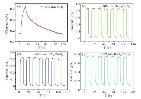
Fig.6.(a)The optical switching characteristic of the ReS2 photodetector at λ =365 nm.(b)–(d)The optical switching characteristic of the ReS2/SnS2 heterostructure photodetector at λ =365-nm,460-nm,and 532-nm wavelengths,respectively.

Table 1.Comparison with reported heterojunction photodetectors.
To compare with other heterojunction photodetectors,Table 1 lists the results of other research groups.[12,17,22,25–29]According to the comparison and analysis in the table, although the response speed of the detector is not as fast as other reported results,the responsivity of the detector is much higher than other reported results,andD*is also about 2–3 orders of magnitude higher than most detectors.In order to improve the responsivity and the response speed of ReS2-based photodetector, the ReS2/SnS2heterojunction is a good choice, and it provides a direction for improving the comprehensive performance of the ReS2-based photodetector.
3.Conclusion
We have achieved an ReS2/SnS2heterojunction photodetector,which presents an ultra-high responsivity of 4706 A/W under 365-nm light irradiation, and the response time is only 1.4 s.In addition, the device also has a high specific detectivity of 5.29×10¹²Jones,an ultra-high EQE of 1.602×10⁶%and an ultra-low noise equivalent power of 1.2×10⁻¹⁶.From the energy band analysis,such a high responsivity is obtained due to the effectively separated electron–hole pairs,which prolongs the lifetime of the carriers, thereby increasing the photocurrent.In conclusion,our ReS2/SnS2heterostructures photodetector provides a new way to improve the responsivity of ReS2-based photodetector and shorten the response time of a single ReS2photodetector.
Acknowledgements
Project supported by the National Natural Science Foundation of China(Grant Nos.61574011,60908012,61575008,61775007, 61731019, 61874145, 62074011, and 62134008),the Beijing Natural Science Foundation(Grant Nos.4182015,4172011, and 4202010), and Beijing Nova Program (Grant No.Z201100006820096).The authors would like to thank the Nano Fabrication Facility, Vacuum Interconnected Nanotech Workstation at Suzhou Institute of Nano-Tech and Nano-Bionics, Chinese Academy of Sciences, and Laboratory of Nanodevices and Applications,Suzhou Institute of Nano-Tech and Nano-Bionics, Chinese Academy of Sciences for their technical supports.
猜你喜欢
Chinese Physics B(2022年10期)2022-10-26
Chinese Physics B(2021年2期)2021-03-11
当代工人(2018年24期)2018-03-29
青春岁月(2017年6期)2017-05-13
环球时报(2016-12-08)2016-12-08
延河(2016年1期)2016-02-26
语文知识(2015年11期)2015-02-28

- Chinese Physics B的其它文章
- Dynamic responses of an energy harvesting system based on piezoelectric and electromagnetic mechanisms under colored noise
- Intervention against information diffusion in static and temporal coupling networks
- Turing pattern selection for a plant–wrack model with cross-diffusion
- Quantum correlation enhanced bound of the information exclusion principle
- Floquet dynamical quantum phase transitions in transverse XY spin chains under periodic kickings
- Generalized uncertainty principle from long-range kernel effects:The case of the Hawking black hole temperature