
Active control of surface plasmon polaritons with phase change materials
2023-11-02 08:10YuanZhenQi漆元臻QiaoJiang蒋瞧HongXiang向红andDeZhuanHan韩德专
Chinese Physics B 2023年10期
Yuan-Zhen Qi(漆元臻), Qiao Jiang(蒋瞧), Hong Xiang(向红), and De-Zhuan Han(韩德专)
Department of Physics and Chongqing Key Laboratory for Strongly Coupled Physics,Chongqing University,Chongqing 401331,China
Keywords: surface plasmon polaritons,phase change materials,direction control,non-diffractive
1.Introduction
Surface plasmon polaritons (SPPs) are electromagnetic excitations emerging from the coupling between photons and free electrons,propagating at the metal-dielectric interface.[1]They offer unique opportunities for manipulating light on a nanoscale,[2]which has important applications in areas such as signal processing, nanoscale imaging, lithography, photovoltaics, and sensing.[3-9]The ability to control of SPPs allows the tuning of SPP behavior to achieve desired effects,improving the performance and functionality of the devices.Controlling the propagating direction of SPPs is a fundamental subject.A variety of approaches have been proposed to control the propagating direction of SPPs.In the early time,passive methods based on Bragg reflection[10]interference between SPPs from slits,[11,12]magnetic antennas,[13]dislocated grating,[14]and asymmetric SPP coupling with aperiodic groove arrays[15]are proposed to achieve unidirectional launching of SPPs.Compared with the passive methods, the active approaches are very favorable for dynamic SPPs functionalities.The active direction control can be realized by manipulating the exciting light, such as the polarization,[16-19]incidence angle[20,21]and the position of the dipole source.[22]The active control can also be done by tuning the active plasmonic material itself.For example, by tuning the conductivity of graphene via electrostatic doping, slowdown and trapping of SPPs,[23]high extinction ratio SPP modulation[24]are achieved successfully.Such an active control also enable the reversible unidirectional SPP launching.[25]
Another effective way of implementing active SPP control is to introduce the phase-change materials(PCMs)which change their optical properties significantly during phase transitions, like VO2and GST (Ge2Sb2Te5or Ge3Sb2Te6).[26,27]VO2undergoes a structural transition at about 68°C, leading to drastic changes in electronic conductivity and optical permittivity.[28]Thus VO2has been widely used in energy storage and optical switching applications.[29,30]GST has distinct refractive index changes between its amorphous state and crystalline state, exhibiting fast switching speeds and good thermal stability.[31]Comparing with VO2, the phase transition of GST is nonvolatile reconfigurable, which means that it can maintain its state for a long time without consuming any energy.[32]Several schemes for unidirectional SPPs have been reported.For example, using the drastic change of the refractive index and absorption coefficient of GST, the unidirectional propagation of SPP can be switched on and off effectively.[33,34]Reversible active switching of SPP directivity via thermally induced phase transition of VO2has also been demonstrated recently.[35]
In this study, we employ a PCM to actively control the propagation of SPPs,and showcase its efficacy in achieving directionally switchable focusing and generating non-diffractive SPP beams.First, a nanoantenna pair containing a PCM is designed to achieve one-way launching of SPPs through interference,with the launching directions corresponding to the amorphous and crystalline states of the PCM being opposite.Next we show that the propagating direction of an SPP beam generated by a linear nanoantenna array can be continuously tuned by changing the crystallinity of the PCM via temperature control.Then we demonstrate active focusing of SPPs by using a circular arc nanoantenna array.We also present the possibility of achieving directional switching of SPP focusing with two back-to-back arranged arc nanoantenna arrays.In the end, we show that a non-diffractive cosine-Gauss SPP beam can be generated by a V-shaped nanoantenna array,and the two back-to-back arranged V-shaped nanoantenna arrays can achieve the directional switching of the cosine-Gauss SPP beam.
2.Tunable one-way launching of SPPs by nanoantenna pair
Figure 1(a) shows schematically the nanoantenna pair constructed on the gold film deposited on an SiO2substrate,with part of geometry parameters marked.Both nanoantennas possess a metal-insulator-metal structure, with one consisting of Si as the insulator and the other employing GST.For convenience, they are called the Si antenna and the GST antenna thereafter,respectively.When anx-polarized plane wave is vertically incident on the structure from above, magnetic resonance will be induced in the metal-dielectric-metal structure,which in turn excites SPPs in the meta film to propagate dominantly in thexdirection.[27]Owing to the interference between the nanoantennas, SPPs may be launched asymmetrically in thexdirection,leading to the possibility of one-way SPP launching in certain circumstances.
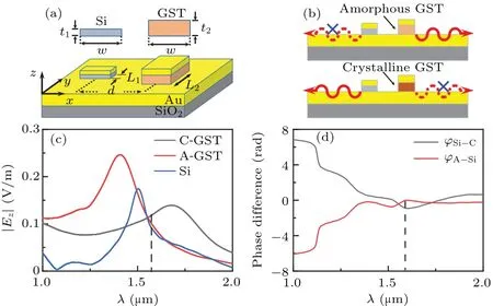
Fig.1.(a) Schematics of (a) nanoantenna pair and (b) one-way launching of SPPs.Wavelength responses of (c) single nanoantennas represented by the electric field(|Ez|)and(d)excited SPPs and phase differences between them,respectively.Here φA-Si=φA-φSi and φSi-C=φSi-φC.The dash lines in panels (c) and (d) suggest the operating wavelength (1.56 µm) in this work.
For a single nanoantenna,as its size is much smaller than the wavelength,it can be regarded as a point source.Then the field of the excited SPP can be expressed in a dipole form[36]
whereEis the initial amplitude,θis the position angle with respect to thexaxis,andδis the propagation distance of SPPs.For a pair of nanoantennas separated by a distance ofd,the observed SPP is the result of the interference of the SPPs excited by the two single nanoantennas.The initial phase of SPPs generated by the GST nanoantenna in the crystalline state and amorphous state are denoted asφCandφA, respectively.As the refractive index of Si is insensitive to temperature,the initial phase of the SPP excited by the Si nanoantenna,φSi, is set to a temperature-independent constant.Owing to the fact that the propagation distance of SPPs is much longer than the distance between the two nanoantennas (δ ≫d), when GST is in the amorphous/crystalline state,the intensity of the SPPs propagating in the±xdirections can be written, respectively,as[12]
Here, superscript (i)/(ii) represents the amorphous/crystalline state of GST in the nanoantenna pair,while superscript(A)/(C)and subscript A/C refer to the single nanoantennas.According to Eqs.(1)and(2),if the following conditions:
The conditions above can be satisfied by choosing appropriate parameters for the nanoantennas.Using the finitedifference time-domain(FDTD)method,we obtain Figs.1(c)and 1(d),which display the amplitudes and phase differences of the SPPs excited by the single nanoantennas, respectively.In the FDTD simulation, thex-polarized light wave propagates along the-zdirection, and the incident position is set toz=2.2µm.The perfectly matched layer absorbing boundary conditions are employed in all directions.The minimum mesh step is set to 0.00025µm.The extra mesh covered region is added outside the nanoantenna structures in all simulations.The corresponding geometry parameters are as follows.The thickness of the gold film deposited on the SiO2substrate is 1 µm.The thickness of the top gold layer in the antenna is 0.05 µm.The width of the two nanoantennasw=0.18 µm.The length of the Si nanoantennaL1=0.1µm and the thickness of the Si layert1=0.05µm.For the GST nanoantenna,the lengthL2=0.3 µm and the thicknesst2=0.2 µm.As can be seen,at the vicinity ofλ=1.56µm,the amplitudes of SPPs excited by the Si nanoantenna and the GST nanoantenna,both the amorphous and crystalline states, are very close to each other, satisfying Eq.(3).Meanwhile, the corresponding phase differenceφSi-φCapproximately equalsφA-φSi, as required by Eqs.(4)and(5).Then,the distance between the two nanoantennas is obtained to bed ≈0.87µm,fulfilling Eqs.(4)and(5).
The proposed structure can be fabricated by using the two-step lithography method[37]as two different dielectric layers exist simultaneously.First the gold film is to be evaporation-deposited on the SiO2substrate.Then, according to the standard electron-beam lithography (EBL), the Si layer and the gold layer of the Si antennas can be fabricated by plasma-enhanced chemical vapor deposition(PECVD)and evaporation deposition,respectively.After removing the photoresist,the second lithography process for the GST antennas is conducted and thus the structure is obtained.Such a fabrication process can be applied to the structures mentioned later.

Fig.2.One-way launching of SPPs at λ =1.56 µm, showing top views of field intensity (|Ez|2) in z=0 plane for (a) amorphous state and (b) crystalline state, respectively, and [(c), (d)] their corresponding side views (Ez)in y=0 plane,with dash boxes in panel(a)indicating the area of calculating extinction ratio.
Figure 2 shows the field distribution of the excited SPPs on the gold film when the antenna pair is illuminated by a normally incident plane wave at a wavelength ofλ=1.56 µm withxpolarization.Figures 2(a)and 2(c)display the field intensity (|Ez|2) in thez=0 plane, and figures 2(c) and 2(d)show the field profiles (Ez) in they=0 plane.When GST is in the amorphous state as shown in Figs.2(a) and 2(c), SPPs propagate unidirectionally rightwards , with an extinction ratio of 69,which is the ratio of the average intensity of the two dash boxes in Fig.2(a).When GST is in crystalline state as shown in Figs.2(b)and 2(d),SPPs propagate unidirectionally leftwards,and an extinction ratio over 1600 is obtained.Thus,the one-way launching of SPPs is achieved for the antenna pair with amorphous GST or crystalline GST.In fact,our calculation shows that the one-way propagation of SPP can be achieved in a range of wavelengths.For instance, an extinction ratio over 20 can be realized in a wavelength range from 1.54µm to 1.57µm.Therefore,the antenna pair can serve as components of device,promoting tunable directional SPPs.
3.Tunable directional SPP beam by liner nanoantenna array
As a single antenna pair works as a directional point source, we use a linear array of nanoantenna pair to generate SPP beams with improved directivity and intensity.As an example, a linear array containing 41 nanoantenna pairs is considered as shown in the inset of Fig.3(c).The distance between neighboring antenna pairs is 0.35µm.The refractive index of the GST can be continuously adjusted by changing the crystallinity via temperature manipulating,[34]hence the propagating direction of SPPs can be tuned flexibly.Figure 3(a) shows the refractive indices of GST at five distinct crystallinities,[38]while figure 3(c) exhibits five field profiles of SPPs generated by the linear antenna array with the corresponding GST at a wavelength of 1.56µm.At the amorphous state of GST,SPP propagates dominantly to the right.With the increase of the crystallinity of the GST,propagations of SPPs occur in both directions, with the SPP on left side enhanced and that on the right side weakened.When GST is completely crystalized, SPP propagates almost entirely to the left.The propagation directivity can be described by the distinction ratio: (IL-IR)/(IL+IR), whereILandIRare the averaged intensity in the boxed area on the left side and on the right side,respectively,as indicated in Fig.3(a).Figure 3(b)shows the calculated distinction ratio and the five blue squares correspond to the cases shown in Fig.3(c).Thus, a liner nanoantenna array can be used to actively tune the propagation direction of the SPP beams.

Fig.3.(a)Curves of refractive index versus wavelength of GST at different crystallinities.(b) Distinction ratio versus GST crystallinity of SPP beam.Positive value means that leftward propagation dominates.The blue squares correspond to cases shown in panel (c).The inset is the schematics of the linear nanoantenna array.(c) Field distributions (|Ez|2) of SPPs excited by the linear nanoantenna array with GST at distinct crystallinity indicated in panels (a) and (b).The dimension of the profiles are 40 µm×15 µm.The dash boxes indicate the calculating areas for the distinction ratio.
4.Tunable focusing of SPPs
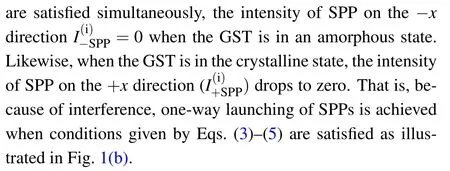
When the nanoantenna pairs are arranged in an arc shape as illustrated in Fig.4(a),the focusing of SPP can be realized.As shown in Fig.4(b),when the GST is fully crystalized,SPPs are well focused in the center of the arc.Similarly, by varying the crystallinity of GST, we can control the focusing of SPPs flexibly as illustrated in Figs.4(b) and 4(c).To quantitatively describe the focusing,we normalize the field intensity at the focal point to the field intensity of GST in an amorphous state.Figure 4(a)shows the normalized focusing intensity, with three blue squares representing the cases presented in Figs.4(b)-4(d).It is evident that the focusing intensity can be continuously adjusted.
In order to enable bidirectional switching of SPP focusing, we introduce a back-to-back configured arc nanoantenna array,which is shown in an inset between Figs.4(e)and 4(f).Note that the constitutional antenna pairs within both arcs share the same orientation.Figure 4(e)demonstrates that left side focusing is attained and the SPP on the right side nearly disappears when GST is in an amorphous state.Conversely,when GST is in a crystalline state, SPP concentrates on the right side while the intensity on the left side is almost zero as depicted in Fig.4(f).The intensity ratios of the left focal point to the right focal point are 410 and 1/524 for the above two cases,respectively.
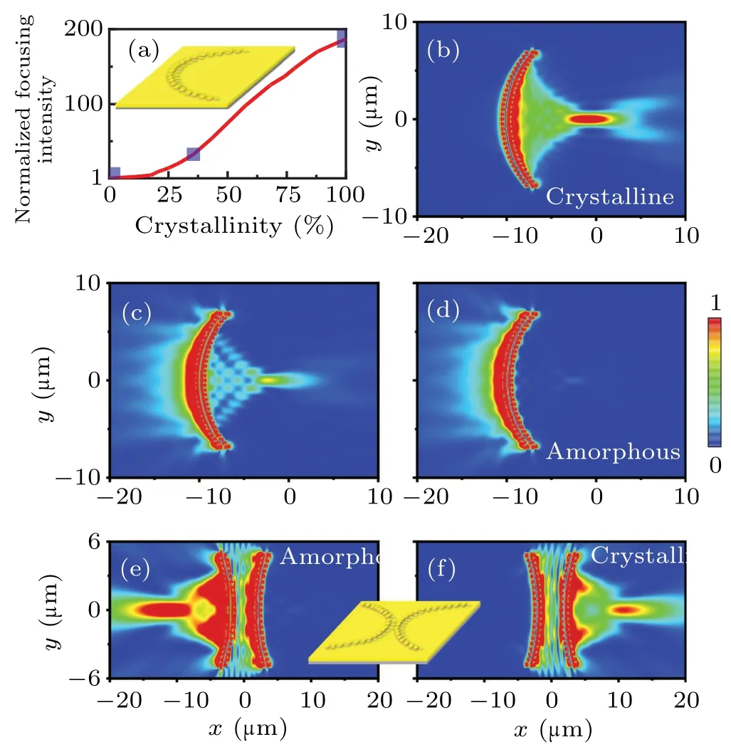
Fig.4.(a)Normalized field intensity versus crystallinityat focal point.The blue squares correspond to the cases shown in panels(b)-(d).The inset shows the designed circular arc nanoantenna array composed of 31 nanoantenna pairs.(b)-(d) Intensity distributions of SPPs when GST transforms from crystalline to amorphous states.The inset between panels (e) and (f) is the back-to-back configured arc nanoantenna array composed of 21 nanoantennas pairs.Panels(e)and(f)are intensity distributions of SPPs when GST is in(e)amorphous state and(f)crystalline state.
5.Switching of cosine-Gauss beam
Fig.5.(a)V-shaped nanoantenna array.(b)Intensity distribution of cosine-Gauss SPP beam for GST in crystalline state.Panels(c)and(d)field intensities along dash lines marked in panel (b), with fitted cosine-Gauss functions also plotted.(e) Back-to-back arranged V-shaped nanoantenna array.Intensity distribution of cosine-Gauss SPPs when GST in(f)amorphous state and(g)crystalline state.
Non-diffractive SPP beams which maintain their intensity profile over long distances, have attracted considerable attention owing to their potential applications in nanophotonic devices.Typical non-diffractive SPP beams, such as Bessellike beam[39,40]and cosine-Gauss beam[41]which propagate in a straight line,are of greatest concern.The non-diffractive SPP beam can be generated through the interference of two line sources.[41]Thus we design a V-shaped nanoantenna array,with the two branches serving as line sources,as shown in Fig.5(a).When the GST is in crystalline state,the SPPs propagate to the right,as indicated by the filed distribution shown in Fig.5(b).The transverse intensity distributions along the dash lines marked in Fig.5(b) are shown in Figs.5(c) and 5(d).The profiles exhibit a cosine-Gauss function distributionI(y)=Acos(ay)2exp[-b(y/w)2], whereA,a, andbare the amplitude, spatial frequency, and the beam waist, respectively.The fitted cosine-Gauss functions are also presented for comparison,which fit well with the profiles of the SPP beams.Parameterbhas the same value(0.35)forx=5µm and 9µm,manifesting the non-diffractive behavior.
To achieve switching of the cosine-Gauss SPP beam,we employ two V-shaped nanoantenna arrays arranged in a backto-back configuration as depicted in Fig.5(e).This approach is akin to the one utilized earlier for focusing switching.As shown in Figs.5(f) and 5(g), when the GST is in its amorphous state, the SPP beam propagates to the left, whereas in its crystalline state, the cosine-Gauss SPP beam switches to the right.
6.Conclusions and perspectives
In summary, we have achieved active control of SPPs through the use of GST.The reversible switching of the unidirectional SPP propagation is workable by changing the refractive index associated with the phase transition.Specifically, the one-way launching of SPP is achieved by using a nanoantenna pair when GST is in its amorphous state or crystalline state.This nanoantenna pair can serve as a componenet for active plasmonic device.We have demonstrated that a linear nanoantenna array can generate switchable directional SPP beams,while a circular arc nanoantenna array can realize tunable SPP focusing.Furthermore, we show that two back-toback arranged arc nanoantenna arrays can facilitate the switching of the SPP focusing direction.This approach can also be applied to non-diffraction beam generation and steering.We illustrate that two V-shaped nanoantenna arrays configured in a back-to-back manner can generate a cosine-Gauss beam with switchable unidirectional propagation.
The proposed schemes of active control the SPPs are expected to be experimentally implemented.We can follow the experimental methods of the previous researches.For example, the leakage radiation microscopy and conoscopic detection[14,42]can be applied to exciting and recording the SPPs.The phase transition of the GST can be controlled by an extra pulsed laser of different wavelengths.[43]The tunable directional control of SPPs demonstrated in this work is expected to find more applications in active nanophotonic devices.

- Chinese Physics B的其它文章
- Single-qubit quantum classifier based on gradient-free optimization algorithm
- Mode dynamics of Bose-Einstein condensates in a single-well potential
- A quantum algorithm for Toeplitz matrix-vector multiplication
- Non-Gaussian approach: Withstanding loss and noise of multi-scattering underwater channel for continuous-variable quantum teleportation
- Trajectory equation of a lump before and after collision with other waves for generalized Hirota-Satsuma-Ito equation
- Detection of healthy and pathological heartbeat dynamics in ECG signals using multivariate recurrence networks with multiple scale factors