
An accurate analytical surface potential model of heterojunction tunnel FET
2023-11-02 08:13YunheGuan关云鹤HuanLi黎欢HaifengChen陈海峰andSiweiHuang黄思伟
Chinese Physics B 2023年10期
关键词:海峰
Yunhe Guan(关云鹤), Huan Li(黎欢), Haifeng Chen(陈海峰), and Siwei Huang(黄思伟)
School of Electronic Engineering,Xi’an University of Posts and Telecommunications,Xi’an 710121,China
Keywords: surface potential model,thermal injection method,tunnel field-effect transistor,heterojunction
1.Introduction
Tunnel FETs (TFETs) have been broadly investigated throughout the past decade years because they can deliver<60 mV/decade subthreshold swing (SS) at room temperature.[1-3]In this way, TFETs are being considered as promising substitutes for MOSFETs in low power applications for future technology nodes.The fabricated III-V heterostructure TFET(H-TFET)with a lateral tunneling junction has demonstrated excellent performance with sub-thermal operation, reaching down to 48 mV/decade, and a high current of 10.6µA/µm at drain-to-source bias of 0.3 V.[4]The TCAD predicted III-V H-TFET with a trench gate and InGaAs pocket structure achieves simultaneously 921µA/µm on-current and average subthreshold swing of 4.9 mV/dec.[5]
Despite significant experimental and finite-element simulation efforts,[4-12]an accurate analytical model of the TFET is urgent and indispensable to provide further insight into the physics of the device and to accelerate the process of device and circuit designs.Furthermore, the potential model is the cornerstone of the capacitance and current models,[13,14]which thus needs to be modeled more accurately.In the promising lateral tunneling TFETs, since the tunneling along the interface between the gate oxide and semiconductor or along the surface of the semiconductor is dominant, the surface potential model is more crucial.[14]If there is no specificity, the TFETs discussed later all refer to the kind with a lateral tunneling junction.There have been many reported surface potential models for TFETs.[15-23]Some of these models assume that the channel is depleted,[15,16]which renders them inapplicable when the device is biased in the drain-control region.Although some models take the effect of the inversion charge into account, they ignore the effects of source depletion,[17-19]meaning the models cannot predict the influence of source doping, which is a key parameter to be designed.[20]Both the inversion charge and source depletion have been considered in other surface potential models, but the potential in the channel is derived based on the Maxwell-Boltzmann(M-B)statistics due to its simplicity.[13,21-23]The M-B approximation works well in the MOSFET modeling,but it leads to considerable deviation in the TFET modeling,[17,24]especially for the characteristic in the drain-control region.
In this paper, an accurate analytical surface potential model for the H-TFETs has been developed,which is validated from the linear region to the saturation region.In Section 2,we derive the surface potential model by solving the 2-D Poisson’s equation on three regions, i.e., the source/channel depletion regions and the channel transport region, considering the fringing field effect from the gate electrodes and the inversion charge from the drain.Then,the validations of the model against the TCAD simulation are presented in Section 3.At last,the conclusion is drawn in Section 4.
2.Model derivation
Figure 1 describes the schematic structure of the doublegate H-TFET considered in this work.In order to obtain the capacitance or drain current expression, an accurate surface potential profile needs to be derived by solving the pseudo-2-D Poisson’s equation first.By TCAD simulation, we get the surface potential profile in the on-state under Fermi-Dirac(FD)statistics as presented in Fig.2.In comparison,the surface potential under the M-B statistic is also shown.Note that the channel is within the inversion state, meaning that the device is biased in the drain-control region.It is apparent that the M-B statistic underestimates the surface potential in the channel since it overestimates the carrier density (inset of Fig.2)and thus the voltage drop over the oxide layer.This means that models based on M-B statistics are inappropriate for predicting the surface potential distribution of TFET,and it is an ample necessity to develop a more accurate surface potential model.

Fig.1.Schematic cross section of the double-gate heterojunction TFET.
From Fig.2, the device can be divided into three parts:source depletion region I with length ofwd,channel depletion region II with the length ofld,and channel transport region III with the surface potential ofφch.If neglecting the effect of the source depletion region,the surface potential in the entire source region is often assumed to be constantφbi(the built-in potential of the source/channel junction).[19]However, from Fig.2, it can be seen clearly that the surface potential in region I varies with location and is not a constant.Since the band-to-band tunneling (BTBT) current is highly sensitive to the band bending at the tunnel junction,[19]modeling the surface potential profile in the source depletion region is of importance to improve the accuracy of the proposed model.The surface potential profile in region Iφs1(x)is given by[20]
whereNS,effis the effective source doping considering the fringing field effect,[25,26]ε1is the dielectric constant of source material,andφbi=-(χ1+Eg1+d1-χ2-0.5Eg2)/q,which is defined as the Fermi level difference between the source and channel materials.The degeneracy factord1is given using Fermi integralF1/2(d1/kT)=(π0.5/2)(NS/NV) withNVbeing the DOS of the source valence band.Egandχare the band gap and electron affinity,and the index of 1 and 2 refers to the source and channel material, respectively.qis the electronic charge.
Now, let us observe Fig.2 again.It can be seen that the surface potential profile in region I obtained by F-D statistics and that by M-B statistics almost coincide although there is an obvious difference betweenφbicalculated by these two statistics.In region I,the carrier density is very low(inset of Fig.2),meaning that F-D statistics can be well approximated by M-B statistics and so can the corresponding surface potential.In Eq.(1),in despite of theφbi,i.e.,the second part of right-hand side(RHS),the depletion widthwd(in first part of RHS)is also dependent on the chosen statistics.From Fig.2,wd(φbi)calculated by F-D statistics is larger(smaller)than that calculated by M-B statistics.Thus,when the F-D statistics is adopted instead of M-B statistics(and vice versa),the influences on these two parts in RHS of Eq.(1)will counteract each other,making the difference inapparent.This also proves the reasonableness of Eq.(1).Moreover, the surface potential profile in region I is very steep with a change of almost 600 meV over a spatial range of about 10 nm,thus the small difference between the FD and M-B statistics will be further submerged and can hardly be observed.

Fig.2.Surface potential profile of the TFET along the channel under F-D statistic.The case under the M-B statistic is also shown by the dashed dot line.The corresponding electron density along the channel is given in the inset.
Since region II is depleted and the inversion charge can be ignored,[26]and therefore 2-D Poisson’s equation can be written as
whereφ2(x,y) is the potential distribution,NCHis the channel doping, andε2is the dielectric constant of the channel material.Using the parabolic approximation along theydirection[26,28]and vertical boundary conditions, Eq.(2) can be transformed into a 1-D second-order differential equation

At the boundary between regions I and II, both surface potential and displacement field have to be continuous,which lead to the following two equations:
From Eqs.(5)and(6),wdandldcan be solved as
with
being the value dropping over region I andφ=qNS,effε1λ2/ε22.Now, in all the parameters, only the surface potential in region IIIφs3is unknown.
According to the thermal injection method(TIM),[17]φs3considering the influence of inversion charge can be expressed as (we kindly ask the reader to see more details about the derivation ofφs3in Ref.[17])
with

However, it should be noted that at a fixedVds,φs3will decrease with the increase ofVgswhenVgsis bigger than some values(defined asVgs,max)as presented in Fig.3(dashed line).This is mathematical but non-physical.Under high gate voltage, the device is within the drain-control region where the surface potential still increases withVgsbut very slowly.[19]Thus,forVgs>Vgs,max,φs3can be approximated to the value atVgs,max.By equaling the differentiation of Eq.(9)to 0,Vgs,maxcan be found as
withFba=qtsNDe(dc-d2)/Vt.Note that during the derivation ofVgs,max,Vris approximated asVcvconsidering that theVgsaround the calculation point is higher.Since this approximation leads to smaller than 0.01%relative error for surface potential(shown in the inset of Fig.3),indicating that Eq.(10)is reasonable.At this time,the surface potential in region III can be finally written as in Eq.(11), and its changes withVgsare plotted in Fig.3(solid line).Now,the dual-modulation effects in TFETs[13,19]are presented well.
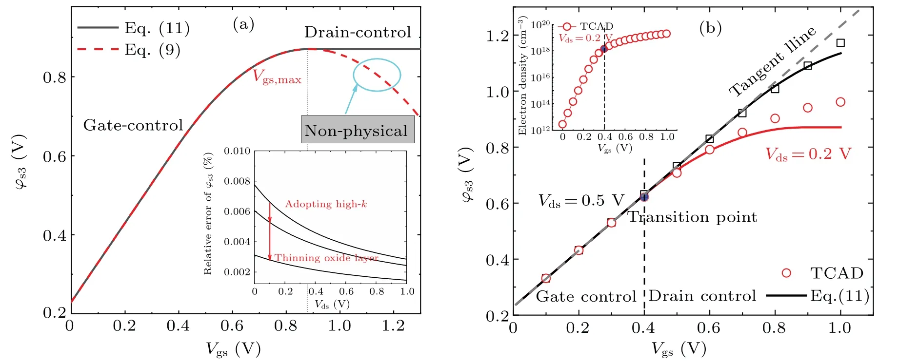
Fig.3.(a)Surface potential in region III φs3 vs.Vgs from Eqs.(9)and(11).The inset presents the relative error of surface potential caused by the approximation of Vgs,max in Eq.(10).(b)The curves of φs3 vs. Vgs from Eq.(11)and TCAD simulation under Vds=0.2 V and 0.5 V.The inset shows the curve of inversion electron density vs.Vgs under Vds=0.2 V.
3.Model validation
Popular combination with GaAs0.5Sb0.5/In0.53Ga0.47As heterostructure is used because it is not only internally latticematched but also lattice matched to the InP substrate.[29]The high-koxide layer HfO2istox= 2 nm thick with dielectric constantεoxof 25.The body thickness ists= 10 nm.The source, channel, and drain regions are p+, p-, and n+ doped, respectively with doping ofNS=5×1019cm-3,NCH=1016cm-3andND=5×1018cm-3.The work function of the gate is 4.6 eV.[30]For the numerical simulations of the test TFET, the commercial TCAD tool Sentaurus-device[31]has been used.The dynamic nonlocal tunneling-path method,F-D statistics, and band-gap-narrowing were activated in the simulations.The quantum confinement effects were ignored for the sake of simplicity as in Ref.[26].The heterojunction interface is assumed to be idealized, because its characteristic would depend on the manufacturing process.Further, the low defect density in the III-V heterojunction has already been demonstrated experimentally through the record highI60=0.31 µA/µm.[4]The parameters for the extraction of the BTBT are taken from Ref.[29], which have been calibrated with the experimental results.
Figure 3(b)shows the dependences of the surface potential in region IIIφs3onVgsunder differentVds,obtained from the model and TCAD simulation.It can be seen that the model can predict the tendency ofφs3withVgsvery well.However,the model underestimatesφs3whenVgsis higher,which can be attributed to two aspects: the adopted TIM method and the piecewise function whenVgs≥Vgs,max.First, it has been demonstrated that the TIM will inevitably underestimate the surface potential when the inversion state is more severe,such as at higherVgsor lowerVds,[17]which results from the uniform distribution assumption of the carrier along theydirection used to perform a calculation ofφs3.Second, from the piecewise function whenVgs≥Vgs,max,φs3is constant and equal to the value atVgs,max, which is inconsistent with the physics.WhenVgsis high, the surface potential still increases,although slowly[19],which can also be observed from Fig.3(b).Therefore,the above two reasons should be both in charge of the deviation ofφs3between the results from the model and TCAD at highVgs.From Fig.3(b), it can also be found that the transition condition between the gate and drain control regions given by the model matches well with that from TCAD simulation.In the drain control region,it has been demonstrated that it is the large amount of inversion electron charge that effectively screens the influence of the gate on surface potential,[19]which can also be illustrated from the inset of Fig.3(b).This indicates that inversion charge cannot be neglected to predict accurately the performance of TFET, especially when it is biased in the drain control region.Furthermore, in the gate control region, the feature of independence onVdsofφs3[19]can also be well predicted by the model.
Figure 4(a)presents the dependence of the surface potential in region III on the drain bias from the TCAD simulation and the model under different gate biases.The tendency ofφs3withVdscan be well predicted by the proposed model.WhenVdsis small, the device is biased in the drain-control region due to the influence of inversion charge, resulting in theφs3increasing withVds.However,at the same time,the inversion charge will disappear gradually with the increase ofVds.When there is no inversion charge in the channel eventually,the drain loses the medium to affect the channel surface potential, and the device is biased within the gate-control region.Therefore,φs3saturates to a value determined by the gate.Meanwhile,the influence ofVgsonφs3can also be predicted from Fig.4(a).It can also be found that with the increase ofVds, the change rate ofφs3becomes higher and finally equal to that ofVgs.For example,whenVgsincrease from 0.3 V to 0.4 V,the increment ofφs3changes from 70 mV to 100 mV at 0.01 V and 0.25 V ofVds,respectively.

Fig.4.(a) The dependence of φs3 on Vds under various Vgs.(b) The comparison of the φs3-Vds curves from the proposed model,and the models from Refs.[18,19]under 0.5 V of Vgs.Symbols and lines are obtained from TCAD and models,respectively.
The deviation from the model to the TCAD data at smallVdscould be attributed to the uniform distribution assumption of the carrier along theydirection when developingφs3.[17]As comparisons, the results from the models in Refs.[18,19]are also plotted in Fig.4(b).Note that these two methods are essentially both based on the M-B statistics.It is apparent that the model based on the adopted TIM is the most accurate to predict the surface potential in the drain control region at a much less computational cost due to that Eq.(11) is fully analytical with no iterative steps.Since the III-V materials,such as InGaAs,have small DOS of the conduction band,severe carrier degeneracy occurs when the inversion layer forms.As presented in Fig.2, at this time the surface potential from the M-B approximation is lower than that from F-D statistics.Thus, the models from Refs.[18,19], as expected, underestimate the channel surface potential at lowVds.However, the calculation ofφs3in this paper is based on the carrier injection from the drain, and thus evades the inaccuracy problems by the M-B statistics.
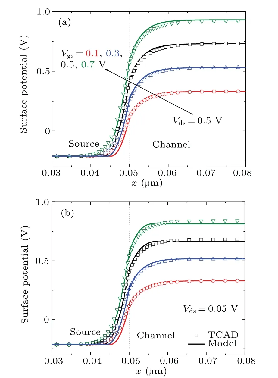
Fig.5.Surface potential profiles obtained from the model (lines) and TCAD(symbols)under different gate voltages at(a)Vds=0.5 V and(b)Vds=0.05 V.
The surface potential distributions along the channel direction are presented in Fig.5 under different biases.Good agreement between the model and the TCAD is achieved.The lengths of region Iwdbecome longer and interface surface potentialφ0becomes larger with increasing gate voltage because of the effect of the gate fringe field.On the other hand,comparing the plots in Figs.5(a)and 5(b),it can also be found that the surface potential will increase with drain voltage when the gate voltage is large.For example,at 0.7 V ofVgs,the surface potential in the channel is equal to 0.84 V and 0.94 V underVds=0.05 V and 0.5 V,respectively.The tendency is consistent with the observation shown in Fig.4.

Fig.6.Electric field profiles obtained from the model (lines) and TCAD (symbols) under different gate voltages at (a)Vds =0.5 V and(b)Vds=0.05 V.
The electric field profiles are shown in Fig.6 under various biases.The electric field becomes stronger with the increase ofVgsdue to the steeper surface potential profiles as shown in Fig.5.The model can also predict the variation of the electric field with biases well.However,it can be observed that there are some mismatches in terms of the maximum value of electric field between the model and the simulation, especially at lowVgs.This can be attributed to the assumption used during the model derivation,i.e.,the electrical field being zero at the interface of regions II and III.From the enlarged electric field profiles in the channel in the inset of Fig.6(a),it is obvious that the field is not zero but with small values, indicating that the surface potential predicted by the model is a bit steeper than that from TCAD.Thus, the zero electric field assumption should be responsible for the mismatch of the maximum electric field.However, with the increase of the gate voltage,the mismatch becomes smaller.For example, whenVgsincreases from 0.1 V to 0.7 V,the relative error of the maximum value between the model and simulation decreases from 28%to 12.5% at 0.5 V ofVds.This is because that the model ignores the vertical part of electric field, which will counteract the impact of zero electric field assumption.The vertical electric field is induced by the concentration gradient of inversion charge along theydirection as shown in Fig.7,and it becomes stronger with the increase ofVgsdue to the higher concentration gradient (Fig.7).Note that the unit of density gradient is a decade per micrometer.As a result, the model matches very well with the simulation in terms of the maximum electric field at highVgs.Furthermore,the better agreement of the maximum electric field between the model and TCAD under all gate voltages at 0.05 V ofVds,as shown in Fig.6(b),validates the above explanation.Since at lowVds, the concentration gradient of inversion charge along theydirection remains high even at 0.1 V ofVgs(Fig.7).Although both assuming zero electric field and ignoring the vertical field will lead to the model underestimating the electric field in the channel,the latter is the dominant attributor at lowVdsand highVgs.This is further validated in Fig.8 with lateral(Ex(x)),vertical(Ey(x)) and total electric field profilesEtotal(x) from TCAD under 0.05 V ofVdsand 0.7 V ofVgs.From Fig.8,it is apparent that it is the vertical part that dominates the electric field in the channel.

Fig.7.Electron density gradient profiles along the y direction from TCAD under (a) Vgs =0.1 V and Vds =0.5 V, (b) Vgs =0.5 V and Vds=0.5 V,(c)Vgs=0.1 V and Vds=0.05 V,and(d)Vgs=0.5 V and Vds=0.05 V.

Fig.8.Total,vertical and lateral electric field profiles along the channel obtained from the TCAD(symbols)underVgs=0.7 V andVds=0.05 V.
At last,we want to clarify that the underestimation of the electric field in region II seems not to influence the model to be used in the current derivation based on the simplified Kane expression,since the uniform distribution of the current along theydirection is often assumed[17,21,22,26]which will balance the impact by this mismatch.
4.Conclusion
In this paper, we develop an analytical and accurate surface potential model for the heterojunction TFET based on the thermal injection method.The influences of inversion charge and source depletion are considered.When comparing with the TCAD simulation results, the model predicts the surface potential and electric field profiles under various biases well.Furthermore, the model has obvious superiority over those based on M-B approximation in terms of the accuracy at a much less computational cost when the device is biased within the drain control region due to the adopted thermal injection method.Although,not discussed in detail here,this proposed model can also be used in homojunction TFET or nanowire structures by adjusting the parameters such as built-in voltage and characteristic length.
Acknowledgements
Project supported in part by the National Natural Science Foundation of China(Grant No.62104192)and in part by the Natural Science Basic Research Program of Shaanxi Province(Grant No.2021JQ-717).
猜你喜欢
当代人(2023年2期)2023-03-17
当代人(2023年1期)2023-02-07
Chinese Physics B(2022年8期)2022-08-31
歌海(2022年1期)2022-03-29
儿童大世界(2019年3期)2019-04-11
歌海(2019年6期)2019-02-22
黄梅戏艺术(2018年1期)2018-07-08
商周刊(2017年25期)2017-04-25
阅读(中年级)(2016年5期)2016-05-14

- Chinese Physics B的其它文章
- Single-qubit quantum classifier based on gradient-free optimization algorithm
- Mode dynamics of Bose-Einstein condensates in a single-well potential
- A quantum algorithm for Toeplitz matrix-vector multiplication
- Non-Gaussian approach: Withstanding loss and noise of multi-scattering underwater channel for continuous-variable quantum teleportation
- Trajectory equation of a lump before and after collision with other waves for generalized Hirota-Satsuma-Ito equation
- Detection of healthy and pathological heartbeat dynamics in ECG signals using multivariate recurrence networks with multiple scale factors