
Perspectives of spin-valley locking devices
2023-11-02 08:37LinglingTao陶玲玲
Chinese Physics B 2023年10期
Lingling Tao(陶玲玲)
School of Physics,Harbin Institute of Technology,Harbin 150001,China
Keywords: spin-valley locking,spintronics,valleytronics,spin-orbit coupling
1.Introduction
Energy extrema of band dispersion in momentum space can be exploited as a new degree of freedom, known as valleys.[1,2]The exploitation and manipulation of valleys have led to the field of valleytronics, which has aroused considerable interest recently due to fundamental interest and potential device applications.[1-3]In analogy to the spin polarization in spintronics,[4]valley polarization is characterized by electron preferentially occupying a single valley.Producing a stable valley polarization is essential for valleytronic applications.Monolayer transition metal dichalcogenides (TMDCs)MX2(M=Mo, W;X=S, Se, Te)[5-7]provide a promising platform to explore the rich valley physics,such as the valley selective circular dichroism,[8,9]the valley Hall effect,[10]the valley Seebeck effect,[11]valley excitons,[12]etc.For example,a large valley polarization of~30%was observed in the pristine monolayer MoS2through optical pumping technique.[9]However,the lifetime of valley polarization induced by circularly polarized photons is very short due to the fast recombination of electron-hole pair.In addition, the valley-polarized current was proposed and demonstrated in graphene nanoribbons and monolayer MoS2via optical or parametric pumping technique[13-17]or by scattering at nonmagnetic disorders.[18]Another efficient way to achieve valley polarization is to lift the valley degeneracy thereby resulting in the valley splitting.Spin-valley locking[19-21]induced by large spin-orbit coupling (SOC) allows control of the valley polarization by lifting the valley degeneracy.Since the two degenerate valleys have opposite spins protected by time-reversal symmetryT,the valley degeneracy can be lifted by broking theTsymmetry to induce spin splitting, which can be realized by using magnetic means such as external magnetic field[22,23]or intrinsic magnetic order.[24-28]
On the electronic device application side, in analogy to spin-valve effect,[4,29,30]valley-valve effect is the change of electrical resistance between two values modulated by valleydependent electron transport.Since the intervalley transport requires the flipping of valley index,the current flowing is expected to be largely suppressed, which yields the high resistance state.In contrast, intravalley transport typically gives rise to relatively low electrical resistance.The valley-valve effect has been predicted for a graphene nanoribbon[31]via local application of a pair of electrostatic potentials as well as WS2/MoS2van der Waals heterostructures.[32]In addition, valley-based logic gates have been proposed in a quasitwo-dimensional (2D) system with merging Dirac cones,which reveal all-electric controlled valley-filter and valleyvalve effects.[33]Recently, Taoet al.[34]proposed valleyspin valves(VSVs)and logic gates based on the strong spinvalley locking effect in certain 2D materials.Using quantumtransport calculations on practical 2D materials-based electronic devices, a giant VSV effect of nearly 100% was predicted for both germanene-and stanene-based VSVs.[34]Further,they proposed the design of valley-spin logic gates by utilizing the predicted giant VSV effect and demonstrated the realization of seven complete logic gates,namely,NOT,XNOR,XOR,AND,NAND,OR,and NOR.[35]More importantly,the proposed valley-spin logic gates satisfy the concatenation requirement, where the output voltage of the logic gate can be used as the logic input for the successive gate.[36]
In this review article, we overview the emerging field of research devoted to spin-valley locking electronic devices.Starting from the basic concepts of valleytronics such as valley polarization and spin-valley locking,we introduce the switchable valley-spin polarization crucial for the design of novel electronic devices.We further discuss the specific materials exhibiting electrically switchable valley-spin polarization.Then we move to the design of valley-spin valves and logic gates.Finally, we outline the perspective of this field of research.
2.Valley-spin valves
2.1.Switchable valley-spin polarization
As previously mentioned,in analogy to spin polarization shown in Fig.1(a),valley polarization characterizes the imbalanced electron or hole occupation numbers between degenerate valleysKandK'shown in Fig.1(b).In the presence of SOC,bands around valleysKandK'reveal Zeeman-type spin splitting,which in turn results in spin-valley locking as shown in Fig.1(c)and observed in TMDCs monolayer.[5]In the case of spin-valley locking,although the net spin polarization and net valley polarization are both zero, the electrons are fully spin-polarized around a given valleyKorK'.Thus, one can define the valley-dependent spin polarization or valley-spin polarization aswhereNdenotes the electron or hole occupation number.From Fig.1(c), one can see that the electrons are fully spinpolarized aroundKorK'valley and the polarity of valley-spin polarization is positive(negative)at theK(K')valley.

Fig.1.Sketches of (a) spin polarization, (b) valley polarization, (c)spin-valley locking and valley-spin polarization, and (d) switchable valley-spin polarization.[35] Arrows denote the spin directions while K and K' denote two valleys, which are related by time-reversal symmetry.(e) Mechanism of switchable valley-spin polarization by electric field E in certain 2D materials with inversion(P)and time-reversal(T)symmetries.[34]
In analogy to switchable magnetization in ferromagnets or switchable polarization in ferroelectrics crucial to the design of non-volatile electronic devices, a natural question to ask is: is it possible to switch the polarity of valley-spin polarization using external means as schematically shown in Fig.1(d)? It is found that the valley-spin polarization for the 2D materials with inversion symmetry and large SOC is indeed switchable by external electric field.[37]As shown in Fig.1(e), we consider the 2D system with inversion (P) and time-reversal(T)symmetries and the band dispersion reveals two well-separated valleysKandK'related byTsymmetry,whereKorK'is a non-time-reversal-invariant momentum.In the absence of external electric fieldE, the band structure is both spin degenerate and valley degenerate (central panel of Fig.1(e))due to the combination ofPandTsymmetries.Application ofEbreaks thePsymmetry and the bands are spin splitting around valleysKandK'by SOC,which results in the spin-valley locking (right panel of Fig.1(e)) and the valleyspin polarizations are opposite between the two valleys as enforced byTsymmetry.Changing the sign ofEis equivalent to thePsymmetry operation,under which the valleyKtransforms toK'(-K)while the spin remains invariant.Thus,the polarity of valley-spin polarization is fully reversed(left panel of Fig.1(e)).Such conclusion is based on the general symmetry analysis and is thus generally applicable.
2.2.2D materials with switchable valley-spin polarization
Having demonstrated the switchable valley-spin polarization based on the general symmetry analysis, we next exemplify this phenomenon in the specific 2D materials based on a tight-binding model or density functional theory (DFT)calculations.As previously demonstrated,[34]the switchable valley-spin polarization by electric field can be realized in a large number of 2D materials such as silicene,[38,39]germanene,[40]stanene,[41,42]1T'-MX2monolayer,[43]and 2H-MX2bilayer (M=Mo, W;X=S, Se, Te).[44]Those 2D materials have inversion symmetry and have been successfully synthesized.Figures 2(a)-2(c)show the calculated band structure for the stanene tunable by electric fieldEz.ForEz=0(Fig.2(a)), a band gap of 0.2 eV is opened at theKandK'valleys by SOC,and the bands are spin and valley degenerate due to the combination ofPandTsymmetries.For finiteEz(Figs.2(b) and 2(c)), the band structure is spin splitting and fully spin polarized around theKandK'valleys.Comparing Fig.2(b) with Fig.2(c) reveals that changing the sign ofEzinterchanges the roles of spin up and down electrons, which in turn switches the valley-spin polarization.Figures 2(d)-2(f)show the DFT calculated electronic structure of 1T'-MoS2monolayer around theKandK'valleys.Similar to the stanene,in the absence ofEz, the band structure exhibits two spindegenerate valleys (Fig.2(d)).Application ofEzsplits the bands into two spin subbands with opposite spin polarizations at the two valleysKandK'(Fig.2(e)).Importantly, the polarity of the valley-spin polarization is reversed by changing the direction ofEz(Fig.2(f)).A similar behavior is also observed for the 2H-MoS2bilayer,as seen from Figs.2(g)-2(i).The spin degeneracy of the two-valley band structure is lifted byEzwith spin polarization being opposite at the two valleys and being reversed with the reversal ofEz.It is seen that the numerical calculations are consistent with above general symmetry analysis.In the above band structure calculations for the stanene and the following quantum transport calculations for the stanene-based electronic devices,the low-energy tightbinding Hamiltonian is given by[45-47]
where the frist term is the nearest-neighbor hopping,is an electron creation (annihilation) operator at the sitei(j)with spinα=↑,↓,tis the hopping parameter and〈i,j〉 denotes the sum over the nearest-neighbor sites.The second term represents the intrinsic SOC with strengthλSO,〈〈i,j〉〉denotes the sum over the next-nearest-neighbor sites,σzis thez-component of the Pauli matrix, andνij=+1 (-1) selects anticlockwise (clockwise) hopping with respect to thezaxis.The third term represents the Rashba SOC induced by an external electric field, and the fourth term is the intrinsic Rashba SOC.Our previous work[34]demonstrates thatλR1is significantly smaller thanλSO, and the intrinsic Rashba SOC(λR2)has a negligible effect.Both Rashba terms are therefore ignored.The last term arises from the applied electric fieldEz,ξi=+1 (-1) distinguishes sitei=A(B), and 2lis theA-Bsublattice buckling height.According to Eq.(1), whenλR1=λR2=0, [σz,H]=0, and the spin componentσzis a good quantum number.The following tight-binding parameterst=1.3 eV,λSO=0.1 eV,andl=0.4 °A are used for the stanene.
2.3.Valley-spin valve effect
The switchable valley-spin polarization can be exploited to design the novel electronic device,this is,valley-spin valve(VSV).Figure 3(a) shows the two-terminal device model for the VSV, where the two regions designated as 1 and 2 serve as a valley-spin polarizer and a valley-spin analyzer, respectively.The working principle for the VSV can be understood from the schematic band alignments shown in Fig.3(b).To be specific,the incoming electrons are neither spin polarized nor valley polarized.In region 1, the application of electric fieldEbreaks the inversion symmetry and results in spin-valley locking so that electrons are spin-up polarized in valleyKand spin-down polarized in valleyK'.In region 2,the valley-spin analyzer selects electrons according to their valley-spin polarization,which can be controlled by the sign ofE.If the field in region 2 is parallel to that in region 1,the valley-spin polarization of the analyzer is the same as that of the polarizer,and both spin-up and spin-down electrons can be efficiently transmitted through the intravalley transport.This configuration is expected to have low resistance(ON state).On the contrary,if the applied field in region 2 is antiparallel to that in region 1,the valley-spin polarization of the analyzer is opposite to that of the polarizer,and either spin electrons encounter a potential barrier for the intravalley transport.Thus, this configuration is expected to produce much higher resistance of the device(OFF state).Such resistance difference between ON and OFF states is dubbed as the VSV effect.
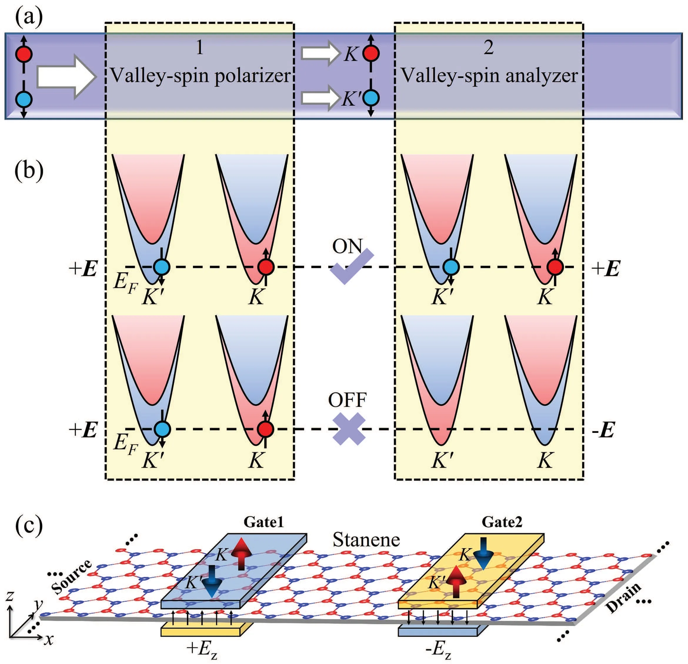
Fig.3.(a)Schematic two-terminal device model for the valley-spin valve.[34]Regions 1 (spin-valley polarizer) and 2 (spin-valley analyzer) are applied with external electric field E.(b) Band alignments between regions 1 and 2.[34]The dashed line indicates the Fermi energy EF.Electrons(filled circles)can either be transmitted(ON state)or blocked(OFF state)depending on the relative orientation of E in regions 1 and 2.(c)Sketches of a stanene-based valley-spin valve device.[34] The two gates of width d1 are separated by distance d2. Ez (black solid arrows) is the electric field generated by the gate voltage.The red and blue arrows denote spin orientations in the K and K'valleys for each gated region.
The feasibility of VSV effect was demonstrated in the stanene-based devices,as shown in Fig.3(c)with double gates placed within the central region.The device state is defined as “parallel” (“anti-parallel”) when the electric fieldsEzare parallel (antiparallel) between gates 1 and 2.VSV conductance ratioηcharacterizing the VSV effect is defined asη=(GP-GAP)/(GP+GAP),withGP(GAP)being the total conductance for the device in the parallel(antiparallel)state.ConductanceGat energyEis calculated by using the Landauer-B¨uttiker formula[48]asG(E)=(e2/h)∑σ,ky Tσ(E,ky),whereeis the electron charge,his the Planck’s constant,Tσis the transmission for spinσ.kyis the transverse Bloch wave vector,which is conserved in the transport process.
Figure 4(a) shows the calculated conductance versus the Fermi energyEFfor parallel(GP)and antiparallel(GAP)states and the resulting VSV conductance ratioη.It is seen that whenEFis close to the conduction band minimumEc,GPis about four orders of magnitude larger thanGAPandηis nearly 100% within the energy window (yellow colored region and Fig.2(c)),indicating a giant VSV effect.Figure 4(b)showsGP,GAPandηas a function ofEzforEF=0.01 eV.As can be seen,the difference betweenGPandGAPincreases significantly with increasingEzand decreases slightly at largerEz.As a consequence,ηincreases significantly and saturates at about 100% after certainEz.It is seen that the giant VSV effect can be achieved in the VSV device constructed by certain 2D materials with electrically switchable valleyspin polarization.More importantly, the giant VSV effect is robust against the disorder due to the well-separatedKandK'valleys.Figure 4(c) shows the averaged conductance and the VSV ratio as a function of disorder strengthW.We assume an Anderson-type disorder in the central region, which is modeled by adding a random on-site potential uniformly distributed in the range from-W/2 toW/2.It is seen that,under weak disorder (W <10 meV), the averaged conductance and the VSV ratioηare nearly independent ofW.When 10 meV<W <100 meV,〈GAP〉increases monotonically with increasingWdue to valley-mix scattering, while〈GP〉 is almost unchanged.WhenW >100 meV,ηdecreases monotonically withW.The shaded area represents the realistic strength of disorder, which produces the sheet resistance of stanene comparable to experimentally measured value.[49]Thus,VSV is largely robust against the disorder scattering.Figure 4(d)schematically shows the electron scattering processes in the AP (OFF) state.We can see that the intravalley scattering is forbidden due to the opposite spin polarizations while the intravalley scattering is allowed contributing to theGAP.However,the twoKandK'valleys are well separated by a wavevector comparable to the size of the Brillouin zone.Thus, intervalley scattering is equivalent to a large momentum transfer,which requires a very strong random potential.Thus,the wellseparatedKandK'valleys are responsible for the robustness of VSV effect against the disorder.
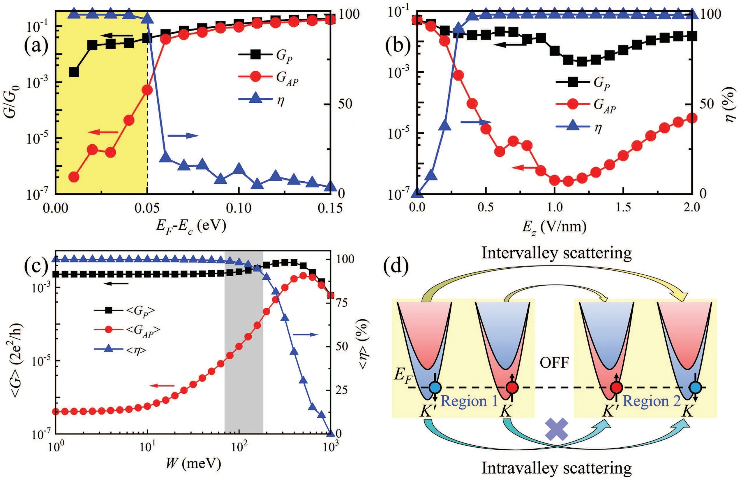
Fig.4.Calculated conductance(GP and GAP)in units of G0=2e2/h(left axis)and VSV conductance ratio η (right axis)as a function of(a)the Fermi energy EF and(b)electric field Ez assuming d1 =100a and d2 =20a.[34] The yellow region in(a)denotes the energy window for achieving a giant VSV effect.(c) Calculated averaged conductance 〈GP〉 and 〈GAP〉 (left axis) and the VSV ratio η (right axis) for stanene as a function of disorder strength W.[34] The shaded region indicates a range of experimentally measured sheet resistances.(d) Schematic intervalley and intravalley scatterings in the AP state(OFF state).
3.Valley-spin logic gates
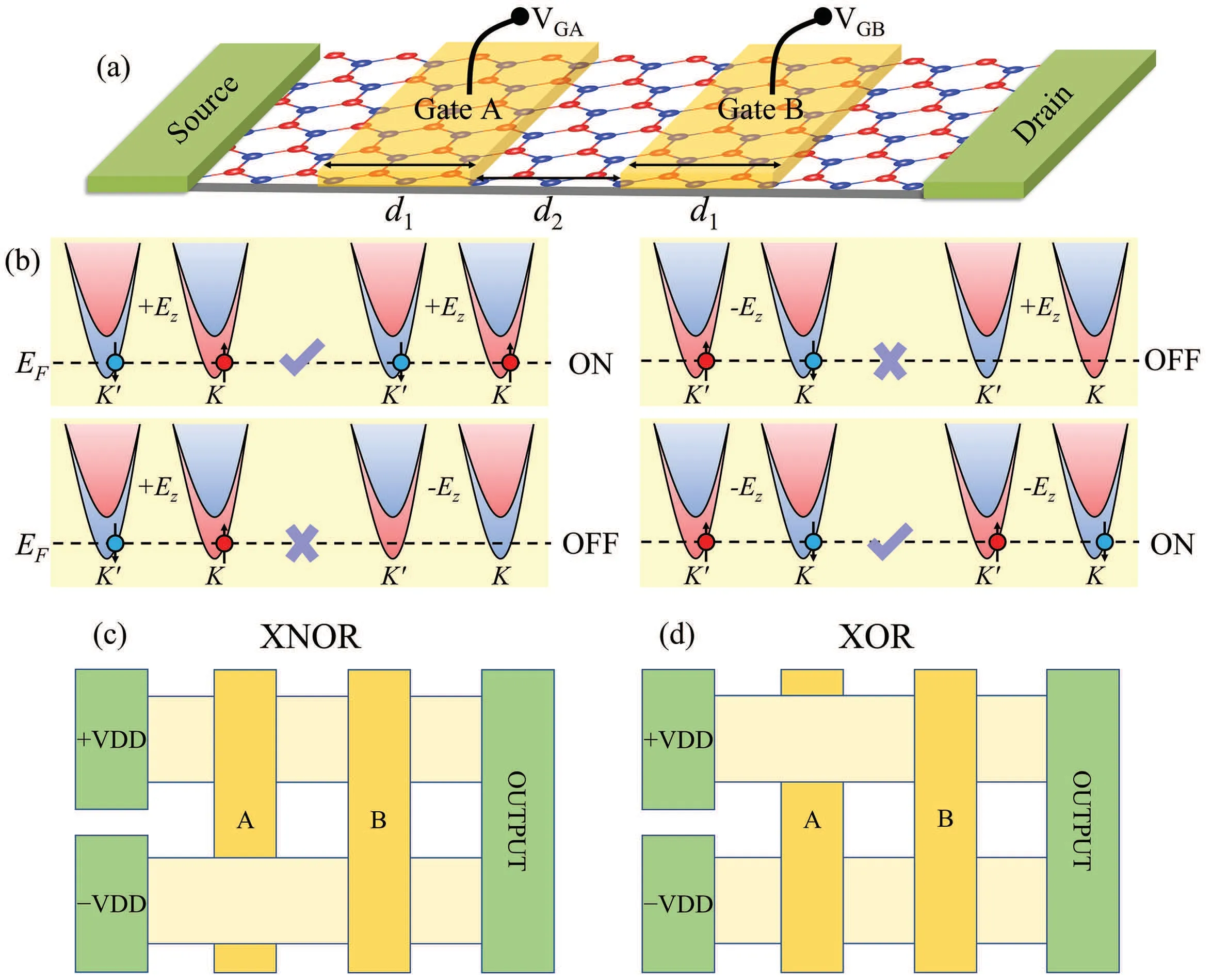
Fig.5.(a)Schematic of the four-terminal device model with two gates A and B.[35]The source and drain are directly connected to the 2D channel.(b)Band alignments at the gate regions for different gate polarities determined by the electric field Ez.[35] Electrons (filled circles) can be transmitted (ON state)or blocked (OFF state) depending on the polarity of Ez in the gated regions.Schematics of(c)XNOR and(d)XOR gates.[35]The light-yellow regions represent 2D channels.Gates A and B act as two logic inputs.Gate A serves as a top gate or back gate,providing an invert of A input in the latter case.VDD is the supply voltage,providing+VDD(-VDD)voltage in the upper(lower)circuit.
One can further design the logic gates based on the VSV device.Figure 5(a) schematically shows a prototype fourterminal building block for the design of XNOR and XOR gates.The source and drain are connected by a 2D channel,whose transport properties are controlled by gates A and B.The logic inputs are encoded by the polarity of gate voltage and positive(negative)voltage corresponds to logic input 1 (0).According to the VSV effect, the device conductance is high (ON state) or low (OFF state) depending on the relative voltage polarities between gates A and B, as schematically shown in Fig.5(b).Figures 5(c) and 5(d) show the designs of XNOR and XOR gates,respectively.A and B serve as logic inputs while the logic output is encoded by the polarity of the output voltage.From Fig.5(c), when the logic inputsA=B=1 or 0,the top circuit is in ON state while the bottom circuit is in OFF state, and the output voltage is+VDD,corresponding to logic 1.When the logic inputsA/=B(A=1,B=0 orA=0,B=1), the top circuit is in OFF state while the bottom circuit is in ON state, and the output voltage is-VDD, corresponding to logic 0.According to the truth table of XNOR gate,the XNOR logic operation is realized.The working principle for XOR gate can be understood in the same way.It is noteworthy that the NOT gate can be realized from the XNOR gate by setting A to 0 or from the XOR gate by setting A to 1.
The design of other logic gates,namely,OR,NOR,AND,and NAND gates, requires a five-terminal building block shown in Fig.6(a),where three gates A,B,and C are involved.Depending on the relative input polarities of the gates,the device can either be in high conductance state (ON state) or in low conductance state(OFF state),as shown in Fig.6(b).Figure 7 shows the designs of OR,NOR,AND,and NAND gates.The working principle for OR gate (Fig.7(a)) can be understood as follows: Control gate CTRL is set to-VDD, and whenA=B=0(-VDD),the two upper devices are in OFF state while the lower one is in ON state.Hence, the output voltage is going to be close to-VDD corresponding to logic state 0.In other cases,the lower device is in OFF state while one of the two upper devices is in ON state.Hence, the output voltage is going to be close to +VDD corresponding to logic state 1.According to the truth table of OR gate, the OR logic operation is realized.The working principles for the other three gates can be understood in the same way.
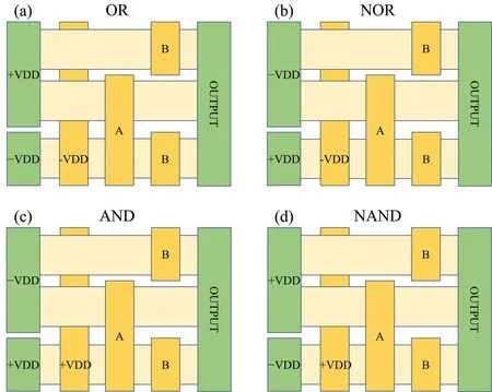
Fig.7.Schematics of (a) OR, (b) NOR, (c) AND, and (d) NAND gates.[35] VDD is the supply voltage.
To summarize, based on the VSV device and giant VSV effect,one can design the seven complete logic gates,namely,NOT,XNOR,XOR,AND,NAND,OR,and NOR.More importantly,the proposed valley-spin logic gates satisfy the concatenation requirement, where the output voltage of the logic gate can be used as the logic input for the successive gate.
4.Summary and outlook
In summary, we have reviewed the recent advances in spin-valley locking physics and device applications, including the valley-spin valves and logic gates.One can define the valley-spin polarization based on spin-valley locking,and more interestingly, certain 2D materials with inversion symmetry and large SOC reveal electrically switchable valleyspin polarization.Such an intriguing property enables valley manipulation by all electrical means and provides an efficient way to control the valley degree of freedom.Switchable valley-spin polarization can be used to design the promising electronic devices such as valley-spin valves and logic gates.For the former,giant VSV effect is demonstrated based on quantum transport calculations on practical 2D materialsbased devices and is robust against the disorder scattering.For the latter, seven complete logic gates, namely, NOT, XNOR,XOR, AND, NAND, OR, and NOR, can be realized.More importantly, the concatenation requirement crucial for programmable logic devices is satisfied.Since the operations of the proposed spin-valley locking devices are based on allelectric means, the fast-switching speed and low-power consumption are expected.[36]
Overall, spin-valley locking is a thriving field of research with extraordinary prospects both for the fundamental physics and for practical applications.Looking forwards, the research of spin-valley locking can be extended into some burgeoning materials such as oxides,[37]van der Waals,[50]moir´e heterostructures,[51-53]topological quantum materials,[54,55]etc.In particular, in ferroelectric materials with large SOC,[37,56-58]the extrema (valleys) of band dispersions such as the conduction band minimum or the valence band maximum are spin polarized.As a result, the spin,valley and ferroelectric polarization are intrinsically coupled, which opens up new avenues of research.In bilayer TMDCs, one could explore the gate-controlled spin-valleylayer locking.[59]In certain 2D ferromagnetic materials, the magnetization and valley are intrinsically locked, which enables the switchable valley-spin polarization by magnetization and results in anomalous valley Hall effect.[60]Moreover,the coupling of the valley and antiferromagnetic order in certain 2D antiferromagnetic materials enables the optical polarization in the spin-valley space,[61]magnetoelectric coupling[62]and the design of novel spin filed effect transistors.[63]Regarding the experimental realization of the proposed spin-valley locking devices, the 2D materials such as germanene and stanene have been successfully synthesized and the doublegate technique has been widely employed in 2D electronic devices.[64,65]To protect the spin coherence against the relaxation crucial for the experimental verification, it is crucial to achieve high-quality materials with minimizing interfacial strains and low defects.In future, one could also explore the spin-valley locking in topological quantum materials[54,55]and design novel electronic devices[66]based on topological protection.
Acknowledgements
The author acknowledges E.Y.Tsymbal and A.Naeemi for the previous collaboration on the related works.This work is supported by the Fundamental Research Funds for the Central Universities(Grant No.FRFCU5710053421)and the National Natural Science Foundation of China (Grant No.12274102).
- Chinese Physics B的其它文章
- Single-qubit quantum classifier based on gradient-free optimization algorithm
- Mode dynamics of Bose-Einstein condensates in a single-well potential
- A quantum algorithm for Toeplitz matrix-vector multiplication
- Non-Gaussian approach: Withstanding loss and noise of multi-scattering underwater channel for continuous-variable quantum teleportation
- Trajectory equation of a lump before and after collision with other waves for generalized Hirota-Satsuma-Ito equation
- Detection of healthy and pathological heartbeat dynamics in ECG signals using multivariate recurrence networks with multiple scale factors