
Intrinsic Limits of Electron Mobility inModulation-Doped AlGaN/GaN 2D Electron Gas by Phonon Scattering
2014-03-24 05:40LiangPang
Liang Pang
Intrinsic Limits of Electron Mobility in
Modulation-Doped AlGaN/GaN 2D Electron Gas by Phonon Scattering
Liang Pang
——We theoretically present the intrinsic limits to electron mobility in the modulation-doped AlGaN/GaN two-dimensional electron gas (2DEG) due to effects including acoustic deformation potential (DP) scattering, piezoelectric scattering (PE), and polar-optic phonon scattering (POP). We find that DE and PE are the more significant limiting factors at intermediate temperatures of 40 K to 250 K, while POP becomes dominant as room temperature is approached. Detailed numerical results are presented for the change of electron mobility with respect to temperature and carrier density. We conclude that these three types of phonon scattering, which are generally determined by the material properties but not the technical processing, are hard limits to the 2DEG mobility.
Index Terms——AlGaN/GaN, 2-dimensional electron gas, electron mobility, phonon scattering.
1. Introduction
Over the past decade, GaN and related nitrides have been intensively studied for the fabrication of high temperature, high power, and high frequency electronic devices, due to the material properties such as high critical breakdown field, high saturation electron velocity, good chemical inactivity, and thermal stability. The most prominent example is the high electron mobility transistor (HEMT), in which the two-dimensional electron gas (2DEG) at the AlGaN/GaN interface greatly enhances the electron mobility[1]~[3]. Because of the large conduction band discontinuity between AlGaN and GaN, and the strong polarization-induced electric field at the interface, the AlGaN/GaN quantum well provides enhanced quantum confinement compared to AlGaAs/GaAs counterpart[4]. Two ways are proposed to dope the structure in order to supply carriers in the 2DEG channel, naming uniform-doping as in Fig. 1 (a) and modulation-doping as in Fig. 1 (b)[5]. Theadvantage of modulation-doping technique is that nearly all the carriers are spatially separated from their donor impurities, which strongly suppresses the impurity scattering effect. Consequently, the 2DEG carrier mobility is further enhanced, making the system a good candidate for high-frequency devices like the HEMTs. However, other scattering effects largely influence the transport properties of the 2DEG carriers. The significance of different scattering mechanisms under different conditions like temperature and electron sheet density, and the limitations that these mechanisms may have on the device performance are crucial from both physical and technical points of view[6]. The three phonon scattering types investigated in this paper are acoustic deformation-potential scattering (DP), piezoelectric scattering (PE), and polar-optical phonon scattering (POP), which are the dominant scattering mechanisms for temperature higher than 40 K. We study their physical importance, summarize their analytical expressions, and investigate their impacts on the electron mobility under different temperatures or 2DEG sheet densities. The purpose of this review is to facilitate a better physical understanding of these particular scattering mechanisms, while emphasizing that it is these three intrinsic material properties that determines the fundamental limit of carrier mobility for any given material systems.
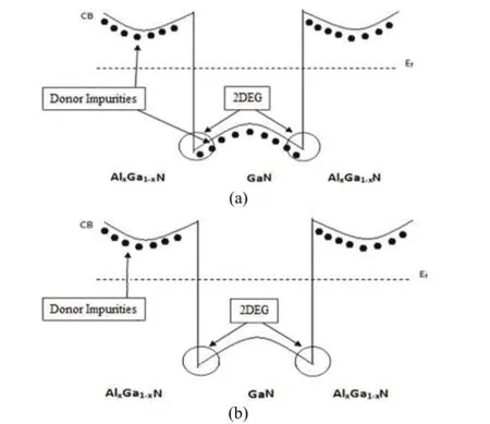
Fig. 1. Conduction band diagram of (a) a uniformly-doped AlGaN/GaN/AlGaN heteostructure and (b) a modulation-doped AlGaN/GaN/AlGaN heteostructure.
2. Scattering Mechanisms
The electron mobility, defined byμn=eτ/m*, whereeis the electronic charge,τis the relaxation time, andm*is the effective electron mass, is a critical transport property. Although not the focus of this study, it should be noted that interface-roughness scattering, as well as alloy disorder and dislocation scattering, which are more process-determined factors, are important scattering mechanisms limiting the mobility. Remote modulation-doping scattering from the ionized impurities in the AlGaN layer is considered negligible because of the strong screening applied to the 2DEG. Consequently, we concern ourselves here only with DP, PE, and POP.
2.1 Acoustic Deformation-Potential Scattering
The relaxation rate for DP is expressed as[7]

where

is a variational parameter,vlis the longitudinal acoustic phonon velocity,EDis the deformation potential,m*is the effective electron mass,kBis the Boltzmann constant,Tis the temperature,ρis the mass density,his the Plank constant,eis the electron charge,nsis the conduction electron concentration,ε0is the vacuum permittivity, andεsis the relative permittivity. The origin of (1) is briefly discussed here.
The variational parameterbcomes from the Fang-Howard wave function[8]

which is used for triangular potential wells and in our case appropriately describes the confinement profile of electrons in the 2DEG. Based on the typical acoustic deformation-potential electron scattering rate in 3D,SIII[9], the scattering rate for 2D electrons,SII, is given by[10]
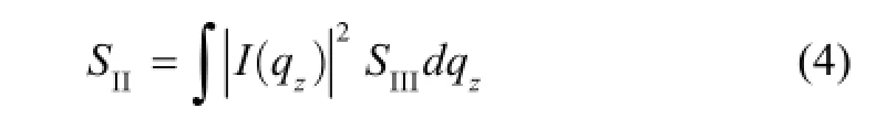
whereq=|k-k′ |,qzis thez-component ofq, andI(qz) is given by[10]

By solving the Boltzman transport equation for low electric fields and using the principle of detailed balance, we can applySIIto a 2D linearized version of the Boltzman equation. Assuming the equi-partition regime, then the phonon occupation number isNq, which can be approximated bykBT/ħωq. If we also assume that the acoustic phonon scattering is elastic, thenħωqdrops out of the Dirac delta function insideSII. With these assumptions, the solution to the Boltzman equation will yield (1). It should be noted that the solution to the Boltzman equation also yields an integral factor term that depends on the angle betweenkandk′. However, this term is not included in our calculations since it can be approximated to unity.
2.2 Piezoelectric Scattering
For the temperature range used in this study, the relaxation rate for PE is given as[11]

wherekF=(2πns)1/2is the norm of the Fermi wave vector,It=[(8ħvtkF/3πkBT)2+1]1/2,Il=[(8ħvlkF/3πkBT)2+1]1/2,zis the average distance of the electronic wave function from the AlGaN/GaN interface corresponding to the lowest sub-band (i.e. the width of the quantum well),h14is the piezoelectric constant, andvtis the transverse acoustic phonon velocity. The piezoelectric effect is resulted when an electrical potential is generated in response to a mechanical stress. This occurs in GaN due to the lack of inversion symmetry (i.e. GaN has a non-centrosymmetric crystalline structure) such that an elastic strain will result in a polarization of the unit cell[12]. Piezoelectric scattering is the additional coupling between the acoustic phonons and the free carriers caused by this potential. GaN along with other nitrides have relatively large piezoelectric constants among III-V semiconductors, so the piezoelectric scattering must be taken into account. Here we will examine (6) to determine the dependence of piezoelectric scattering on temperature and electron sheet density.
2.3 Polar-Optical Phonon Scattering
For POP, the relaxation rate is expressed as[14]

is the effective dielectric constant,ħωPOPis the polar optic phonon energy,k0=(2m*ħωPOP/ħ2)1/2is the electron wave vector corresponding to the phonon energy,NB(T)=1/[exp(ħωPOP/kBT)-1] is the phonon occupation number described by the Bose-Einstein distribution, andfPOP=1+(1-exp(-y))/yis a function with a dimensionless variabley=πħ2ns/m*kBT. The value ofG(k0) is determined from the Fang-Howard wave function as[14]

POP is an important mechanism in GaN and other III-V compounds because of the opposite ionic charges on the two atoms. A distortion in the crystal lattice will result in a macroscopic field that scatters the electrons. The longrange potential results in a scattering rate matrix element that is inversely proportional to|k-k′|.This means that the scattering prefers small angles and we do not have therandomized collisions. As a result, one cannot make the same simplifications for the Boltzman equation as with DP. But we will, as with the other scattering mechanisms, analyze its dependence on temperature and electron sheet density.
3. Analytical Results
The mobilities determined by DP, PE, and POP are calculated from the respective relaxation rates given in (1), (6), and (7) along with the equationμn=eτ/m*. The values of different GaN parameters used in the calculation are listed in Table 1. The total mobility is obtained using the Mathiessen rule as
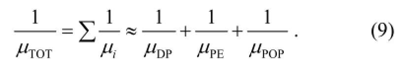

Table 1: Values of GaN parameters used in calculation
Fig. 2 shows the calculated mobility as a function of temperature with an electron sheet density (ns) of 1.3×1017cm-3. It can be observed that DP and PE are important at the intermediate temperature (T=40 K to 250 K), while POP becoming more significant at higher temperature (T= 250 K to 300 K), since the dependence ofuPOPon temperature is determined byfPOP(y)/NB(T). This makes sense because higher temperatures are needed in order for the phonon occupation number,NB(T), corresponding to polar optical phonons, to reach an appreciable value. We comment on the fact that the curve for total mobility in Fig. 2 does not flatten out at lower temperatures because of the omission of other scattering mechanisms like interface-roughness scattering, which dominate the mobility at low temperatures.
Fig. 3 shows the calculated mobility as a function of electron sheet density forT=300 K. The effect of electron sheet density for DP is determined from (1) by the variational parameter in the Fang-Howard wave function,b. Sincebis proportional tons1/3,μDPis proportional tons-1/3, which is shown by the curve forμDPin the figure. For PE, we note that the relationship betweenμPEandμDP,along with the Fermi wave vector,kF, determines the effect of sheet density on PE. SinceμPEis proportional toμDP/kfand the Fermi wave vector is proportional tons1/2, the result isμPEbeing proportional tons1/6. Last but not least, we obtained the relationship between POP andnsby determining the effect thatnshas onfPOP(y) andG(k0). ForT=300Kand the given parameters, we find thatfPOP(y) is a decaying function for the given range ofns.G(k0) also has a dependence on the electron sheet density because it is determined by using the Fang-Howard wave function. By examining the equation forG(k0), we find that it is responsible for 43% decrease inμPOPwhen increasingnsfrom 1×1016cm-3to 9×1016cm-3, whilefPOP(y) being responsible for 57% of the decrease. Therefore, both factors are important in determining the dependence ofμPOPonns.

Fig. 2. Calculated mobilities for DP, PE, and POP, as well as the corresponding total mobility as a function of temperature forns=1.3×1017cm-3.
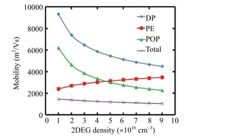
Fig. 3. Calculated mobilities for DP, PE, and POP, as well as the corresponding total mobility as a function of electron sheet density atT=300 K.
4. Conclusions
In this review, we have investigated the transport properties of a modulation-doped AlGaN/GaN 2DEG system. For intermediate to high temperatures (T=40 K to 300 K), the important scattering mechanisms, including DP, PE, and POP, are analyzed and calculated as the function of temperature and electron sheet density. We conclude that DP and PE are the dominant mobility limiting mechanisms for intermediate temperatures, while POP becoming more significant near the room temperature. Besides thedependence of PE on the width of the quantum well, these scattering mechanisms are intrinsic to the material. Thus, they are essential in determining the fundamental limit of carrier mobility for any chosen material systems. Advances in the deposition and processing of 2DEG systems may reduce or even eliminate the contribution of scattering mechanisms like interface-roughness scattering, impurity scattering by unintentional background charged impurities, and remote modulation-doping scattering, but the effects of DP, PE, and POP for a givenTandnsare indeed the material properties that cannot be ignored or reduced.
[1] U. K. Mishra, P. Parikh, and Y. F. Wu, “AlGaN/GaN HEMTs: An overview of device operation and applications,”Proc. IEEE, vol. 90, pp. 1022-1031, Jun. 2002.
[2] L. Pang, H. C. Seo, P. Chapman, I. Adesida, and K. Kim,“Breakdown voltage enhancement of AlGaN/GaN high-electron-mobility transistors via selective-area growth for Ohmic contacts over ion implantation,”J. Electron. Mater., vol. 39, pp. 499-503, May 2010.
[3] L. Pang, and K. Kim, “Bimodal gate-dielectric deposition for improved performance of AlGaN/GaN metal-oxidesemiconductor high-electron-mobility transistors,”J. Phys. D: Appl. Phys.,vol. 45, no. 4, pp. 045105-045110, Jan. 2012.
她经常凝望自己的脸。在酒店或者餐厅洗手间的镜子里,在商店的试衣镜里,在家里梳洗台的镜子里,见到不同时刻的面容,疲惫的,隐忍的,衰竭的,意兴阑珊的。她想认清和确定自我的来源和实质。而那个新的自我,是脸颊上膨胀出两团胭脂红晕的女子。年少时,做爱之后脸颊就会变得这样红,微醺而烂熟的云霞般绚烂沉醉的红晕。她害怕失去这种敏感而独特的身体反应。
[4] R. Dingle, H. L. Stormer, A. C. Gossard, and W. Wiegmann, “Electron mobilities in modulation-doped semiconductor heterojunction superlattices,”Appl. Phys. Lett., vol. 33, pp. 665-667, Oct. 1978.
[5] Z. W. Zheng, B. Shen, and Z.-J. Qiu, “Quantum and transport scattering times in modulation-doped AlxGa1-xN/GaN single quantum wells,”Appl. Phys. A, vol. 80, pp. 39-42, Jan. 2005.
[6] T. Kawamura and S. Das Sarma, “Low-temperature energy relaxation in AlxGa1-xAs/GaAs heterojunctions,”Phys. Rev. B, vol. 42, no. 4, pp. 5407-5410, Sep. 1990.
[7] D. S. Zanato, N. Balkan, B. K. Ridley, and W. J. Schaff,“The effect of interface-roughness and dislocation scattering on low temperature mobility of 2D electron gas in GaN/AlGaN,”Semicond. Sci. Technol., vol. 19, pp. 427-430, Mar. 2004.
[8] B. Podor, “Improved variational wave function for triangular quantum wells and its effect on the scattering rate,” inProc. of Int. Semiconductor Conf., 1995, pp. 267-270.
[9] K. Hess,Advanced Theory of Semiconductor Devices, Piscataway, New Jersey: Wiley-IEEE Press, 2000.
[10] T. Kawamura and S. Das Sarma, “Phononscattering-limited electron mobilities in AlxGa1-xAs/GaAs heterojunctions,”Phys. Rev. B, vol. 45, pp. 3612-3627, Feb. 1992.
[11] K. Lee, M. S. Shur, T. J. Drummond, and H. Morkoc, “Low field mobility of 2-D electron Gas in modulation doped AlxGa1-xAs/GaAs layers,”J.Appl.Phys., vol. 54, pp. 6432-6438, Nov. 1983.
[12] G. Martin, A. Botchkarev, A. Rockett, and H. Morkoc,“Valence-band discontinuities of wurtzite GaN, AlN, and InN heterojunctions measured by x-ray photoemission spectroscopy,”Appl. Phys. Let., vol. 68, pp. 2541-2543, Feb. 1996.
[13] J. C. Cao, and W. Y. Yao, “Linear and nonlinear electron transport in modulation-Doped AlGaN/GaN heterostructures,”Jpn. J. Appl. Phys., vol. 43, pp. 50-53, Jan. 2004.
[14] B. L. Gelmont, M. Shur, and M. Stroscio, “Polar optical-phonon scattering in three-and two-dimensional electron gases,”J.Appl. Phys.,vol. 77, pp. 657-660, Jan. 1995.

Liang Pang was born in Nanjing, China in 1985. He received his B.Eng. degree in electrical and electronics engineering in 2008 from Nanyang Technological University, Singapore, the M.S. degree in electrical and computer engineering in 2010, and the Ph.D. degree in electrical and computer engineering in 2013, both from the University of Illinois, Urbana, USA. He is currently a senior device engineer at SanDisk Corporation. His research interests include GaN-based power electronics and flexible electronics.
Manuscript received October 2, 2013; revised December 20, 2013. This work was supported in part by the Grainger Center for Electric Machinery and Electromechanics of the University of Illinois.
L. Pang is with the Department of Electrical and Computer Engineering, University of Illinois, Urbana 61801, USA. (Corresponding author e-mail: danielangp@ gmail.com).
Digital Object Identifier: 10.3969/j.issn.1674-862X.2014.04.014
猜你喜欢
星星·散文诗(2021年22期)2021-12-21
星星·诗歌原创(2021年8期)2021-08-31
少年文艺·开心阅读作文(2020年10期)2020-10-20
智族GQ(2019年1期)2019-05-14
小小说月刊(2019年4期)2019-04-18
电子制作(2018年18期)2018-11-14
火花(2015年1期)2015-02-27
理科考试研究·高中(2014年9期)2014-09-22
丝绸(2014年12期)2014-02-28
丝绸(2014年2期)2014-02-28
 Journal of Electronic Science and Technology2014年4期
- Journal of Electronic Science and Technology的其它文章
- Study on Temperature Distribution of Specimens Tested on the Gleeble 3800 at Hot Forming Conditions
- Non-Linearity of Visual Sensitivity and Pursuit Velocity during Smooth Pursuit Eye Movements
- Automatic Vessel Segmentation on Retinal Images
- Family Competition Pheromone Genetic Algorithm for Comparative Genome Assembly
- Quantification of Cranial Asymmetry in Infants by Facial Feature Extraction
- Real-Time Hand Motion Parameter Estimation with Feature Point Detection Using Kinect