基于五轴平台的非展开曲面导电图形3D打印方法
2018-04-13 06:36:32赵家勇刘大川赵鹏兵黄进谢鹏志宫剑刘朋朋
现代电子技术
2018年8期
赵家勇 刘大川 赵鹏兵 黄进 谢鹏志 宫剑 刘朋朋
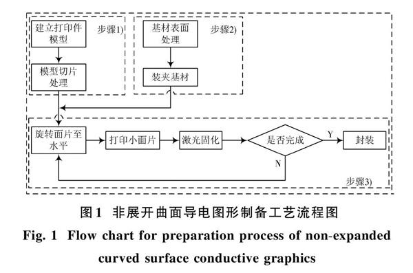


摘 要: 非展开曲面导电图形是在非展开曲面上形成的具有导电特性的特定图形,其制备是共形天线、频率选择表面、可穿戴电子产品制造中的关键步骤之一。传统上普遍采用先制作平面导电图形再拼接的方法,存在成形精度低、导电性能差等缺陷,为此,提出一种基于五轴联动平台和喷印技术的非展开曲面导电图形三维打印方法,开发了相应的工艺并研制了装备。实验结果表明,基于该方法制备的非展开曲面导电图形的成形精度可达±0.1 mm、厚度均匀性误差小于4%、导电率可达1×10⁷ S/m,为高性能共形微带天线、频率选择表面的研制提供了一种有效的技术途径。
关键词: 非展开曲面; 导电图形; 五轴联动; 喷印技术; 三维打印方法; 微带天线; 频率选择表面
中图分类号: TN917.8?34; TN605 文献标识码: A 文章编号: 1004?373X(2018)08?0010?03
Abstract: The non?expanded curved surface conductive graphics is a specific graphics formed on the non?expanded curved surface with conductive properties, whose preparation is one of the key steps of manufacturing conformal antennas, frequency selective surfaces and wearable electronic products. Traditionally, the method of first making a conductive plane graph and then splicing is universally adopted, but it has some defects such as low forming precision and poor electrical conductivity. Therefore, a 3D printing method based on five?axis linkage platform and jet printing technology is proposed for non?expanded curved surface conductive graphics. The corresponding processes and equipment were developed. The experimental results show that the forming precision of non?expanded curved surface conductive graphics prepared based on the proposed method is ±0.1 mm, the thickness uniformity error is less than 4%, and the conductivity can be up to 1×10⁷ S/m, which provides an effective technical way for manufacturing conformal microstrip antennas with good performance and frequency selective surfaces.
Keywords: non?expanded curved surface; conductive graphics; five?axis linkage; jet printing technology; 3D printing method; microstrip antenna; frequency selective surface
0 引 言
非展开曲面导电图形是在非展开曲面上形成的具有导电特性的特定图形,其制备是共形天线、频率选择表面、可穿戴电子产品制造中的关键步骤之一,随着电子技术的快速发展,将会得到越来越广泛的应用[1]。在三维结构表面制备导电图形,不仅可以提高空间利用率,还可以进一步减小体积,但要求导电图形能与基体结构实现高度融合和集成,且要求导电图形具有良好的电磁性能。传统的制造方式多采用先在平面上制备导电图形,然后通过转印等工艺再将导电图形印制在三维基体表面之上[2],或者使用电镀等方式直接在基体表面制备导电图形[3],但这些方法都存在工艺复杂、耗时长、成形精度差等缺陷。……
登录APP查看全文