
Synthesis and characterization of β-Ga2O3@GaN nanowires∗
2019-02-25 07:22ShuangWang王爽YueWenLi李悦文XiangQianXiu修向前LiYingZhang张丽颖XueMeiHua华雪梅ZiLiXie谢自力TaoTao陶涛BinLiu刘斌PengChen陈鹏RongZhang张荣andYouDouZheng郑有炓
Chinese Physics B 2019年2期
Shuang Wang(王爽),Yue-Wen Li(李悦文),Xiang-Qian Xiu(修向前),Li-Ying Zhang(张丽颖),Xue-Mei Hua(华雪梅),Zi-Li Xie(谢自力),Tao Tao(陶涛),Bin Liu(刘斌),Peng Chen(陈鹏),Rong Zhang(张荣),and You-Dou Zheng(郑有炓)
Key Laboratory of Advanced Photonic and Electronic Materials,School of Electronic Science and Engineering,Nanjing University,Nanjing 210023,China
Keywords:β-Ga2O3@GaN,nanowires,thermal oxidation
1.Introduction
GaN[1]is a wide direct-bandgap semiconductor with characteristics including low electric constant,high electrondrift velocity and high thermal conductivity while monoclinic β-Ga2O3[2,3](Eg=4.9 eV)has high breakdown voltage,low on-resistance,favorable chemical and thermal stability.Both GaN and Ga2O3are widely used in optoelectronic and power devices.[4-8]In recent years,GaN/Ga2O3composite nanostructures have drawn more attention,due to their large surfaceto-volume ratio,rapid charge carrier separation and high operating temperature.[9-13]GaN@Ga2O3hetero-structures have been reported[9,10],but β-Ga2O3@GaN nanowires have been rarely reported.The β-Ga2O3shell can be obtained by oxidation of GaN or epitaxy of β-Ga2O3.Since the thermal oxidation method has been proved to reduce interface trap density with low cost and simple operation,it is a preferable method to obtain β-Ga2O3by oxidizing GaN.[14]Considering the combination of outstanding properties of the two materials,the β-Ga2O3@GaN structures have potential applications in fabrication of novel nano-devices.This core-shell structure is expected to promote the sensitivity,selectivity and operation temperature of detectors and hydrogen evolution efficiency in photoelectric chemical water splitting.[15-17]
In this study,we reported the detailed process of β-Ga2O3@GaN nanowires from GaN NWs by thermal oxidation.The surface morphologies,crystal structure,and optical properties of β-Ga2O3@GaN NWs were systemically investigated.
2.Experimental details
GaN NWs were grown on single-layer graphene/sapphire substrates by chemical vapor deposition(CVD)using Ni catalyst at 1100°C for 5 min.High-purity gallium metal and NH3were used as the sources of Ga and N,respectively.Before the growth of GaN NWs,the substrate pretreatment was carried out at 1100°C for 15 min in an NH3atmosphere.The oxidation process of GaN NWs was accomplished in an O2flow of 200 sccm at 900°C,950°C,and 1000°C for different oxidation times(5 min,10 min,and 20 min).Then,β-Ga2O3@GaN NWs and fully-converted β-Ga2O3NWs were obtained.
The morphology,structural and optical properties of samples were characterized by scanning electron microscopy(SEM),x-ray diffraction(XRD),Raman spectroscopy,transmission electron microscopy(TEM),and photoluminescence(PL)spectra.
3.Results and discussion
3.1.Morphology and structure property of GaN NWs
Figure 1(a)presents the SEM morphology of GaN NWs.The average length and density of GaN NWs are approximately 10µm and 5.4×10⁵per mm2,respectively.The diameter of GaN NWs ranges from 120 nm to 260 nm.It is clearly seen that most of NWs have smooth surfaces.However,a few of the NWs have rough surfaces,which is attributed to a large Ga-source supply in some areas during the vapor deposition process.[18]The high resolution TEM(HRTEM)image of a single GaN NW is shown in Fig.1(b)with clear lattice fringes of GaN,and the selected area electron diffraction(SAED)pattern indicates that the high-quality wurtzite GaN NWs have been obtained.
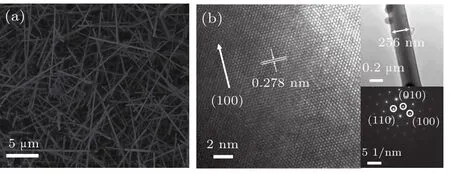
Fig.1.(a)SEM image of GaN NWs and(b)HRTEM image of a single GaN NW.The insets of Fig.1(b)show TEM and SAED images.
3.2.Structure analysis of oxidized NWs
Figures 2(a)and 2(b)show the XRD patterns of the NWs oxidized at 950°C for different times and different temperatures for 10 min,respectively.All the GaN and β-Ga2O3diffraction peakscan be indexed(JCPDS No.50-0792,No.43-1012).The appearance of β-Ga2O3peaks reveals that NWs undergo the phase transformation from wurtzite GaN to monoclinic β -Ga2O3.The peaks of β -Ga2O3become prominent with the increase of the oxidation time or temperature,which meansthatthe oxidation degree hasbeen increased.GaNNWs were partially converted into β-Ga2O3at 950°C for 5 min and 10 min,which is shown in Fig.2(a).Once oxidation time reached 20 min at 950°C or 10 min at 1000°C,GaN NWs were completely converted to β-Ga2O3NWs(the uppermost spectra in Figs.2(a)and 2(b)).The peak intensity of GaN decreases with increasing the oxidation temperature,shown in Fig.2(b),which is because higher oxidation temperature enhances the oxygen diffusion and improves the oxidation rate.The oxidation may be done under the combination mechanism of diffusion and interface reaction:after the adsorption of O2and oxidation of the surface of GaN NWs,O2diffuses through the oxidized region and arrives at the interface between GaN and Ga2O3.Then,the interior GaN is further oxidized.[19-21]During the oxidation process controlled by the combination mechanism,sufficient O2flux,high temperature and atmospheric pressure make GaN NWs continuously oxidized.
Figures 3(a)and 3(b)show the Raman spectra of GaN NWs and the oxidized NWs at 950°C for different times and different temperatures for 10 min,respectively.The E2(high)peak at 568 cm-1from GaN implies that GaN NWs are stressfree.[22]In particular,because of the N-rich GaN configuration and the zone-boundary phonons,the peak at 420 cm-1is also observed.[22,23]While the oxidation time is 20 min at 950°C or 10 min at 1000°C,the Raman peaks corresponding to GaN disappear and only Raman peaks of β-Ga2O3can be observed.These phonon modes are derived from the vibration and translation of the GaIO4chains,deformation of the GaIO4and GaIIO6and stretching and bending of the GaIO4.[24]Some of the β-Ga2O3peaks coexist with GaN peaks while the oxidation time is shorter or oxidation temperature is lower,which suggests that the NWs are composite structures of GaN and β-Ga2O3.The above results are consistent with the XRD analysis.
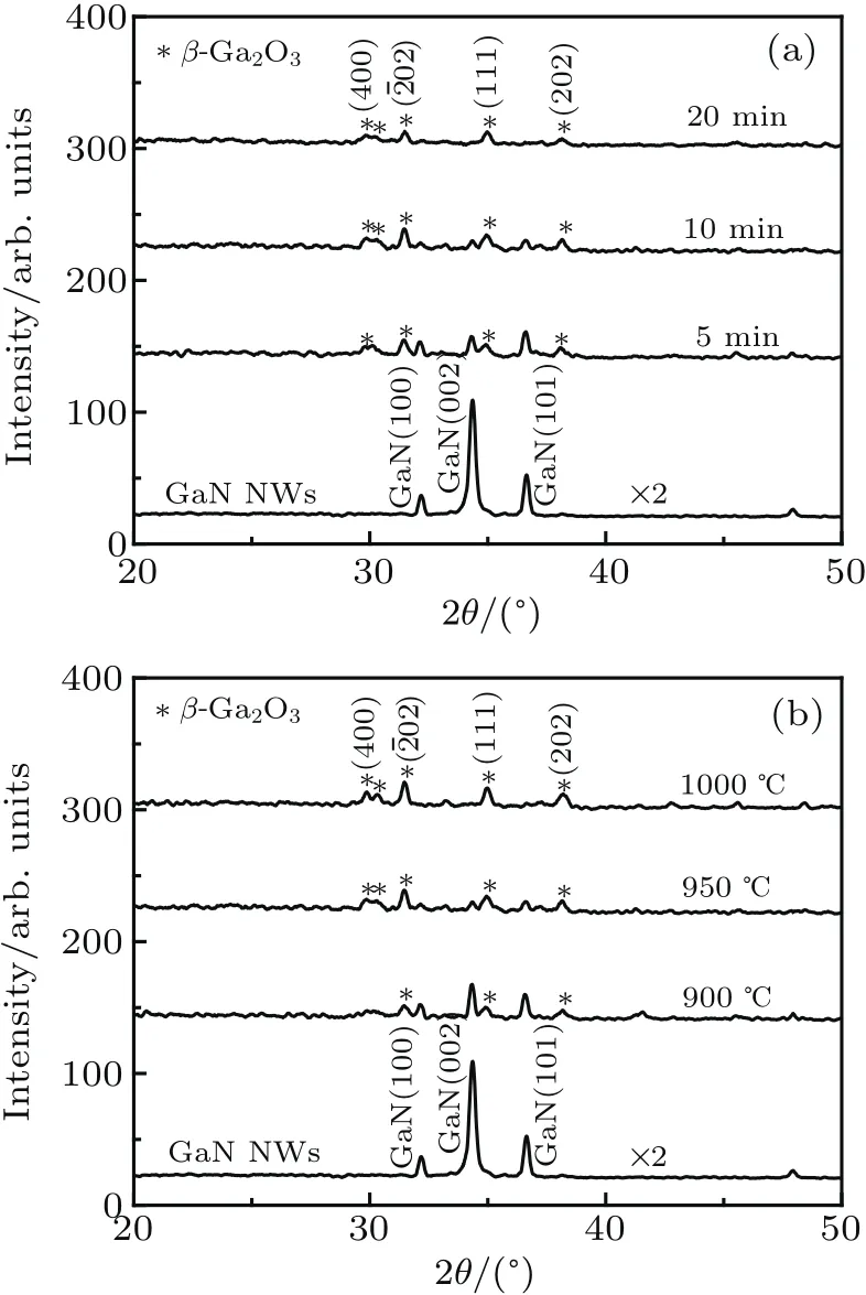
Fig.2.XRD patternsof GaN NWs and the samples after oxidation at(a)950°C for different times(5 min,10 min,and 20 min)and(b)different temperatures(900 °C,950 °C,and 1000 °C)for 10 min.

Fig.3.Raman spectra of GaN NWs and oxidized NWs formed at(a)950°C for different times and(b)different temperatures for 10 min.
3.3.Optical property of GaN and oxidized NWs

Fig.4.PL spectra of GaN NWs and oxidized NWs formed at(a)950°C for different time and(b)different temperatures for 10 min.
PL spectra of GaN NWs and oxidized NWs were measured at room temperature,as shown in Fig.4.PL spectra are excited with a continuous wave He-Cd laser source.For the GaN NWs,an obvious near band edge emission(NBE)peak is observed at 365 nm.[25]In Fig.4(a),the main emission peak moves to the short wavelength with the increase of oxidation time,due to the oxidation of GaN NWs.The Gaussian fitting of PL spectra indicates that GaN and β-Ga2O3coexist in the NWs after the oxidation at 950°C for 5 min and 10 min.Few defects generated in the oxidation process may result in the GaN-NBE peak shift to∼366 nm(the fit peaks shown in Fig.4).[23,26]While GaN NWs were oxidized at 950°C for 20 min,only the strong UV and blue-green emission peaks of oxidized NWs are observed,which means that GaN NWs were entirely converted to β-Ga2O3NWs.The UV peaks at∼363 nm originate from the recombination of carriers from the lowest oxygen vacancy level and the top of valance band.[27,28]The blue-green peaks are derived from the recombination of electrons from donor bands consisting of oxygen vacancies and holes from acceptor bands consisting of gallium vacancies and gallium-oxygen vacancy pairs by tunnel capture.[29,30]PL spectra of NWs oxidized at different temperatures for 10 min show similar results in Fig.4(b).
3.4.Structure of β-Ga2O3@GaN NWs
Figure 5(a)and 5(b)are the TEM images of GaN NWs oxidized at 900°C for 10 min and 950°C for 5 min.The hexagonal spot array in SAED pattern in the inset of Fig.5(a)suggests that the core of the nanowire is single crystal GaN.The lattice fringes of GaN and β-Ga2O3and the clear coreshell structures can be observed,which means that the β-Ga2O3@GaN structure have been obtained.The oxide shell thicknesses of β-Ga2O3@GaN NWs,as in the insets of Figs.5(a)and 5(b),are calculated to be about 30 nm and 55 nm,respectively.So,the oxidation rate increases from 3 nm/min at 900°C to 11 nm/min at 950°C.TEM images of a fully-converted β-Ga2O3nanowire are shown in Fig.5(c).The SAED patterns imply that β-Ga2O3shells are polycrystalline.The polycrystalline phase may be attributed to the random initial nucleation and rapid growth of β-Ga2O3.[20]The rough surface means the large surface-to-volume ratio,which can provide trap sites of carriers in novel device application.
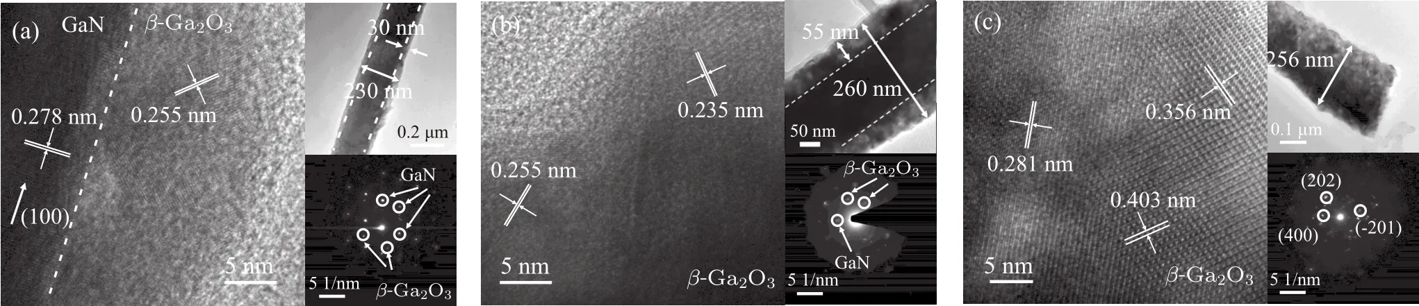
Fig.5.HRTEM images of the oxidation NWs formed at(a)900 °C for 10 min,(b)950 °C for 5 min and(c)1000 °C for 10 min.The insets are the corresponding TEM and SAED images.
4.Conclusion and perspectives
In summary,β-Ga2O3@GaN NWs were converted from high-quality GaN NWs by thermal oxidation.The oxidation temperature and oxidation time have significant in fluence on the oxidation degree of GaN NWs.The β-Ga2O3@GaN NWs are achieved more easily at 900°C while the oxidation at 1000°C is suitable for obtaining fully-converted β-Ga2O3NWs.TEM images and PL spectra show that oxidized NWs are expected to provide large surface-volume and abundant vacancies.β-Ga2O3@GaN structure would have potential applications in sensing and optical devices.
猜你喜欢
文艺生活(艺术中国)(2022年2期)2022-04-21
科技创新导报(2021年31期)2021-05-10
考试与评价·八年级版(2020年3期)2020-11-02
学苑创造·A版(2019年8期)2019-08-15
民间故事选刊·上(2017年2期)2017-02-23
百家讲坛(蓝版)(2017年11期)2017-02-08
小小说月刊·下半月(2017年1期)2017-02-06

- Chinese Physics B的其它文章
- Physics of quantum coherence in spin systems∗
- Recent progress of infrared photodetectors based on lead chalcogenide colloidal quantum dots∗
- Progress in quantum well and quantum cascade infrared photodetectors in SITP∗
- Recent advances in Ga-based solar-blind photodetectors∗
- Development of long-wavelength infrared detector and its space-based application requirements∗
- Transition of photoconductive and photovoltaic operation modes in amorphous Ga2O3-based solar-blind detectors tuned by oxygen vacancies∗