
Effect of temperature on photoresponse properties of solar-blind Schottky barrier diode photodetector based on single crystal Ga2O3∗
2019-04-13 01:14ChaoYang杨超HongweiLiang梁红伟ZhenzhongZhang张振中XiaochuanXia夏晓川HeqiuZhang张贺秋RenshengShen申人升YingminLuo骆英民andGuotongDu杜国同
Chinese Physics B 2019年4期
关键词:杨超
Chao Yang(杨超),Hongwei Liang(梁红伟),†,Zhenzhong Zhang(张振中),Xiaochuan Xia(夏晓川),Heqiu Zhang(张贺秋),Rensheng Shen(申人升),Yingmin Luo(骆英民),and Guotong Du(杜国同)
1School of Microelectronics,Dalian University of Technology,Dalian 116024,China
2State Key Laboratory of Luminescence and Applications,Changchun Institute of Optics,Fine Mechanics and Physics,Chinese Academy of Sciences,Changchun 130033,China
1.Introduction
A solar-blind photodetector is used in the detection of photon signal shorter than 280 nm and scarcely responds to the wavelength above 280 nm.Owing to the strong absorption by the ozone layer,the radiation in the range 200 nm–280 nm emitted by the sun cannot reach the Earth’s surface.[1,2]Therefore,‘zero-background noise’is a prominent advantage for the application of solar-blind wavelength in many communication fields.The solar-blind photodetector is now widely applied in missile warning,corona electrical discharge, fire alarms,ozone monitoring,under water and space communication,and so on.[3–6]
Various wide band gap semiconductors have been investigated to fabricate solar-blind photodetectors,such as β-Ga2O3,AlxGa1−xN,MgxZn1−xO.High Al and Mg composition is,respectively,necessary to modulate the band gap of AlGaN and MgZnO and keeps the photodetector response range in solar-blind wavelength.However,the crystal quality of AlGaN films deteriorates rapidly[1,7–9]and the MgZnO appears phase segregation[10,11]as the Al or Mg composition increases.β-Ga2O3is one of the most suitable materials for solar-blind photodetection because its band gap(Eg)is about 4.9 eV and locates at the center position of the solarblind wavelength without the need of composition modulation.Ga2O3solar-blind photodetectors are mainly fabricated on nanostructure,thin films,and single crystal.Solar-blind photodetectors based on Ga2O3nanostructure are characterized by simple growth and high internal gains.[12,13]Nevertheless,the solar-blind Ga2O3photodetector with large size of detect area or even capability of imaging is desired in many application fields.[6,14,15]Large size and high quality Ga2O3single crystals can be achieved through conventional methods such as floating zone(FZ),[16]edge-defined film-fed growth(EFG),[17]and Czochralski(CZ)[18]methods.Moreover,high quality Ga2O3single crystals can reduce the defects density to a very low level and lower the effect of persistent photoconductivity,and thus increase the device response speed.
A junction-type Ga2O3photodetector,compared with photoconductive type,presents a higher response speed at room temperature(RT).The photoresponse properties of photodetector at higher temperature are even more important in applications such as flame detection.However,few studies of the properties of junction-type Ga2O3photodetector at high temperature have been published.Among the various kinds of junction-type Ga2O3photodetector,a relatively simple preparation process is required for Schottky barrier diode(SBD)photodetector.In this work,the current–voltage(I–V)characteristics,response speed,and solar-blind selectivity of Ga2O3SBD solar-blind photodetector are investigated.Meanwhile,a Cu Schottky electrode with honeycomb porous structure is adopted to the fabrication of solar-blind photodetector.The photodetector presents good rectifying properties at RT and clear photoresponse to the ultraviolet shorter than 259 nm and maintains a high reversibility and response speed,even at 85.8◦C.
2.Experimental details
The commercial(¯201)-orient β-Ga2O3substrate with 600-µm thickness is used to fabricate the SBD photodetector by cutting along the[010]and[102]orientation into 5 mm×5 mm pieces.The unintentional doped Ga2O3crystal is n-type with a carrier concentration of about 1017cm−3.The sample is degreased using methanol(5 min)/acetone(5 min)/methanol(5 min)/deionized water(5 min),successively.Then,the samples are etched in the solution with H2SO4:H2O2:H2O=4:1:1 for 5 min.Finally,the samples are dipped in 90-◦C deionized water.
The metal deposition is performed by vacuum thermal evaporation method.A Ti/Au(20 nm/200 nm)Ohmic contact with 4 mm×4 mm is first deposited on the back side of the substrate and is subsequently thermally annealed at 450◦C in nitrogen for 3 min.Cu is used to prepare Schottky contact because it can form similar effective barrier height to that prepared with Au,[19,20]which is also proven in this work.Moreover,the adhesion property of Cu electrode is much better than Ni and Au in our experiments.The 200-nm Cu electrode is deposited on the top surface of the Ga2O3substrate.Cu Schottky electrodes with a diameter of 0.6-mm are formed to investigate the effect of annealing temperature on the electrical properties of Cu/Ga2O3SBD.Samples are annealed at 100◦C/200◦C/300◦C in nitrogen for 5 min.The I–V characteristics of Cu/Ga2O3SBD obtained from the samples annealed at different temperature show that relatively better rectifying properties can be achieved after being annealed at 200◦C.Consequently,the Cu Schottky electrode of Ga2O3solar-blind photodetector is annealed at 200◦C in nitrogen for 5 min.The Schottky electrode of the photodetector is prepared using standard photolithography and lift-off techniques.The electrode is designed in honeycomb porous structure with diameter of 2.8 mm.Any three adjacent holes can be grouped into an equilateral triangle.The diameter of the holes and spacing between them are 40µm in this experiment and the effect of the size on the photoresponse properties will be investigated in future experiments.The schematic structure of the photodetector is shown in the inset of Fig.1(a).
The I–V characteristics for the SBD are measured using Keithley 4200-SCS semiconductor characterization system.Time-resolved photocurrent response spectra are conducted under 253-nm light with Keithley 4200-SCS semiconductor characterization system.The photoresponse spectra of the photodetectors are measured in an SPEX scanning monochromator employing a 150-W Xe lamp as the illumination source.The responsivity spectrum is obtained by measuring the photocurrent (calibrated with a standard Si photodiode)under the illumination of an Xe lamp spectrum from 200 nm to 500 nm using a scanning monochromator.
3.Results and discussion
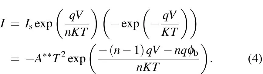
The forward and reverse I–V characteristics of the Cu/Ga2O3SBD annealed at different temperatures are shown in Fig.1. The forward current is linear in the semilogarithmic scale at low forward bias voltages as shown in Fig.1(a).The dominant current transport mechanism can be determined by comparing the thermal energy KT with E00W hen KT?E00,thermionic emission is the dominant transport mechanism.[21]Considering the effect of series resistance Rs,the diode equations can be written as Eq.(1):[22,23]
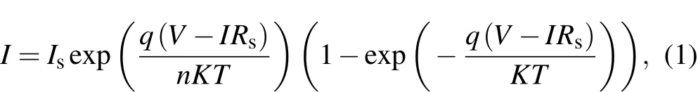
where Is=A∗∗T2exp(−qφb/kT).I,Is,V,K,q,n,A∗∗, φb,and T is current,saturation current density,applied forward bias voltage,Boltzmann constant,elementary charge,ideality factor,effective Richardson constant,barrier height,and temperature,respectively.The effective Richardson constant A∗∗is calculated to be 41.04 A·cm−2·K−2[24]at RT,using electron effective mass m∗=0.342 m0,[25]and free electron Richardson constant A∗=120 A·cm−2·K−2.Fitting this model to the line arrange of the semi-logplot of I versus V,the change trend of φband n of all the samples annealed at different temperatures is shown in Fig.1(c).The sample without annealing(w/o ann.)shows a relatively lower Schottky barrier height.As the annealing temperature increases,the barrier height increases while the ideality factor decreases first and then reaches a minimum(1.145)at 200◦C.When the annealing temperature increases further,the ideality factor increases slightly.The ideality factor results indicate the Cu/Ga2O3Schottky contact is closest to thermionic emission model after annealed at 200◦C.Reverse I–V characteristics are shown in Fig.1(b).The reverse current of the sample without annealing increases dramatically at low bias and shows poor rectifying properties.The current reduces by over two orders of magnitude after being annealed at 100◦C and reaches 10 nA at−48 V.The rectifying properties are improved and a current of 10 nA is obtained at a higher voltage(69 V)after being annealed at 200◦C.The reverse current increases slightly after annealed at 300◦C.
Fig.1.The I–V characteristics of the Cu/Ga2O3SBD annealed at different temperatures:(a)forward I–V curves(the inset is the top view and schematic structure of the photodetector),(b)reverse I–V curves,and(c)the ideality factor and barrier height.
Based on these results,the Schottky contact electrode of the photodetector is annealed in nitrogen at 200◦C for 5 min.The photoresponse spectra of the photodetector are measured at various reverse bias range from 0 V to 42 V.The responsivity of the photodetector can be calculated by Eq.(2):[26]

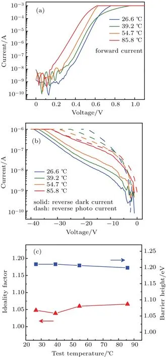
where Rλis the responsivity of the photodetector,Iphotois the photo current,Idarkis the dark current,S is the effective illuminated area,and P is the light intensity.The photoresponse spectra measured at 0 V and 42 V are shown in Fig.2(a).An obvious response can be detected at solar-blind wavelength when zero bias voltage is applied,which proves that the device can be used as a self-powered solar-blind photodetector.The photocurrent at a 0 V bias is the result of the photovoltaic effect.When the reverse bias is elevated to 42 V,the maximum responsivity is about 0.8 A/W.Quantum efficiency η is a function of Rλas Eq.(3):[21,27]
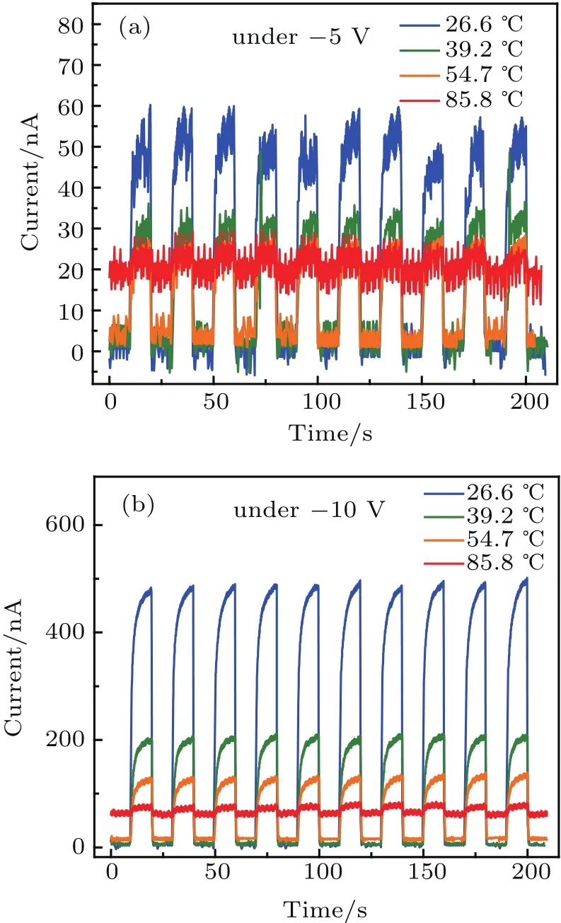
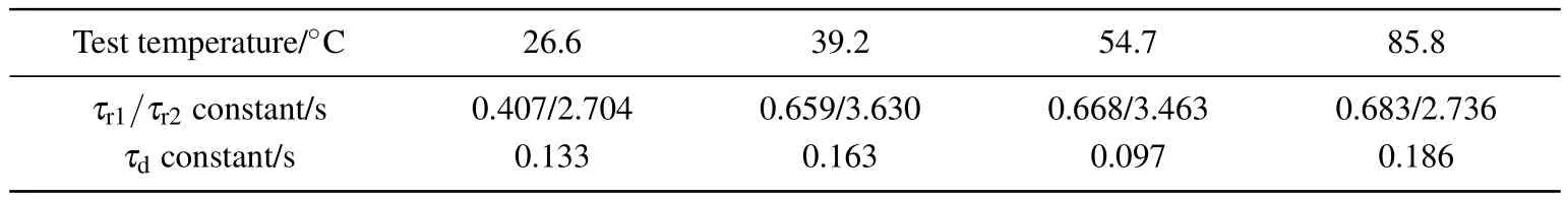
where h is Planck’s constant,c is the velocity of light,e is the basic electron charge,and λ is the incident light wavelength.The quantum efficiency exceeds 100%when the bias is larger than 36 V and reaches 400%at 42 V,which benefits from the honeycomb porous structural Schottky electrode.Although the UV photons are blocked by the region covered with Cu,the area of enhanced electric field in the depletion layer is beyond the edge of the Schottky electrode and forms ring area in the exposed holes to collect the photogenerated carriers.Highly symmetric electrode structure can reduce the concentration of electric field in some large curvature area.The maximum of responsivity and quantum efficiency of the photodetector at each bias are extracted out and the relation between the maximum value and reverse bias voltage is shown in Fig.2(b).As the reverse bias increases,the responsivity increases gradually in the low bias range and then increases dramatically when the bias exceeds 35 V.The increased responsivity in low bias range can be attribute to the widening ring area with enhanced electric field as the reverse bias increases according to the simulation results(not shown here).The dramatically increased responsivity in high bias range is also analyzed in another report,[27]which is attributed to avalanche multiplication mechanism.The positive temperature coefficient of the breakdown voltage is recognized as the criterion to determinate avalanche mechanism.[13,21,28,29]However,no obviously positive shift of breakdown voltage is observed in the reverse dark current as the temperature increases as shown in Fig.3(b),which indicates the response process involved other unknown gain mechanism.A further investigation will be required to obtain a better understanding of this mechanism.The cutoff wavelength and the rejection ratio are two important parameters to characterize the selectivity of solar-blind photodetector.The cutoff wavelength is defined as the ratio between the position of maximum responsivity and the natural constant(e≈2.718).The cutoff wavelength of the photodetector is limited to 259 nm which demonstrates an excellent solar-blind selectivity.The solar-blind/visible(=3213)and solar-blind/UV(=834)rejection ratiosare calculated from the ratio of responsivity at peak to 400 nm and peak to 280 nm,both of which indicate the photodetector scarcely responds to the light out of solar-blind range.A comparison among the reported solarblind photodetectors[30–32]based on single crystal Ga2O3is summarized in Table 1 to analyze the effect of electrode on the photoresponse properties.A uniform semi-transparent electrode with a large area is adopted in the first two reports,both of which show clear response to the light close to and even above 280 nm.This phenomenon can be attributed to the internal photoemission.[21]In this process,electrons in the thin electrode can surmount the Schottky barrier and be collected by the semiconductor due to the excitation of smaller energy photon(qφb Fig.2.Photoresponse characteristics for the photodetector:(a)responsivity of the detector measured under 0-V and 42-V biases,and(b)the relation between the reverse bias and the maximum of responsivity and quantum efficiency. Table 1.Comparison of the photoresponse parameters among the single crystal Ga2O3-based photodetectors. The I–V characteristics of the photodetector is measured from RT to 85.8◦C,as shown in Fig.3.Figure 3(a)shows the forward temperature-dependent I–V characteristics of the photodetector.The ideality factor and barrier height are fitted based on the linear parts in the semilogarithmic scale,and are shown in Fig.3(c).Both the ideality factor and the barrier height are almost a constant(1.05 and 1.20)at RT and higher temperatures,which is also mentioned in other reports.[33,34]An increase of the reverse dark current and a lowering of the reverse photo current with elevated temperature are observed in Fig.3(b).The reason for the increase of dark current can be explained with Eq.(1),which can be written as a form of Eq.(4)under higher reverse bias: The reverse dark current monotonically increases with the elevated temperature.The reason for this lowering of photo current can be attributed to the comprehensive factors of enhanced carrier recombination,[35]stronger lattice scattering,[36]and the narrowing of depletion width WDat high temperatures.The depletion width WDcan be written by Eq.(5)[21] where the εsis dielectric permittivity,NDis doping concentration,and ψbiis built-in potential.The first[33]and third terms in the parentheses decreases as the temperature increases,which weakens the separation of photogenerated electron–hole pairs. The time-resolved photoresponse of the photodetector at different temperatures is carried out under 253-nm illumination by on/off switching.Ten cycles of on/off state current under−5-V and−10-V biases are shown in Figs.4(a)and 4(b),respectively.Although a slight fluctuation of photocurrent is measured at−5 V,the photodetector shows a high response speed—especially in the decay edge.When the reverse bias is set to−10 V,the 10-periods photocurrent is stabilized at around 500 nA.As the temperature increases,the photocurrent shows almost no fluctuation.This proves the high reversibility and high reproducibility of the photodetector.Both the rise time curve and decay time curve can be fitted with a secondorder exponential formula[37,38] Fig.3.The I–V characteristics of the photodetector measured at different temperatures:(a)forward I–V curves,(b)reverse I–V curves under dark and illumination,and(c)the ideality factor and barrier height. where I0is the steady state photocurrent,t is the time,A and B are constants,τ1and τ2are two relaxation time constants corresponding to a fast-response component and a slow-response component.The constant τ1is related to the rapid change of the carrier concentration when the UV light is turned on/off,and τ2is related to carrier trapping and releases due to the oxygen vacancy defects.[39,40]The sharp decay edge results in two equal relaxation time constants,which means the formula is simplified to be I=I0+Ae−t/τd.The relaxation time constants are fitted based on time-resolved photocurrent plots at different temperatures under−10-V bias,as shown in Table 2.Both the rise time and decay time constant show almost no change as the temperature increases,which indicates a stable response speed of the photodetector at elevated temperature. Fig.4.Time-resolved characteristics of the solar-blind Cu/Ga2O3SBD photodetector measured at:(a)−5 V and(b)−10 V. Table 2.The rise time constant τrand decay time constant τdat different temperatures at−10-V bias. A vertical structural SBD solar-blind photodetector is fabricated on a single crystal Ga2O3.The effect of annealing temperature on Cu/Ga2O3Schottky contact properties is investigated and the Schottky electrode of the photodetector is annealed at200◦C in nitrogen for 5 min.The quantum efficiency of the photodetector can reach 400%at 42 V.High solar-blind selectivity of the photodetector is demonstrated by a sharp cutoff wavelength at 259 nm with high solar-blind/visible(=3213)and solar-blind/UV(=834)rejection ratio.Both the quantum efficiency and sharp cutoff wavelength benefit from the honeycomb porous structure Schottky electrode.The I–V characteristics and time-resolved photoresponse of the photodetector are investigated at 253-nm illumination from RT to 85.8◦C.Both of the ideality factor and barrier height are almost constant(1.05 and 1.20)at RT and higher temperatures.Although the elevated temperature leads to an increased dark current and decreased photocurrent,the photodetector main-tains a high reversibility and response speed—even at high temperatures. [1]Sang L,Liao M and Sumiya M 2013 Sensors 13 10482 [2]Razeghi M and Rogalski A 1996 J.Appl.Phys.79 7433 [3]Razeghi M 2002 Proc.IEEE 90 1006 [4]Monroy E,Omn`es F and Calle F 2003 Semicond.Sci.Technol.18 R33 [5]Xu Z Y and Sadler B M 2008 IEEE Commun.Mag.46 67 [6]Li J,Zhou Y,Yi X,Zhang M,Chen X,Cui M and Yan F 2017 Curr.Opt.Photon.1 196 [7]Walker D,Kumar V,Mi K,Sandvik P,Kung P,Zhang X H and Razeghi M 2000 Appl.Phys.Lett.76 403 [8]Tut T,Gokkavas M,Inal A and Ozbay E 2007 Appl.Phys.Lett.90 163506 [9]Parish G,Keller S,Kozodoy P,Ibbetson J P,March,H,Fini P T,Fleischer S B,DenBaars S P,Mishra U K and Tarsa E J 1999 Appl.Phys.Lett.75 247 [10]Fan M M,Liu K W,Chen X,Wang X,Zhang Z Z,Li B H and Shen D Z 2015 ACS Appl.Mater.Interfaces 7 20600 [11]Wang L K,Ju Z G,Zhang J Y,Zheng J,Shen D Z,Yao B,Zhao D X,Zhang Z Z,Li B H and Shan C X 2009 Appl.Phys.Lett.95 131113 [12]Zhao B,Wang F,Chen H,Zheng L,Su L,Zhao D and Fang X 2017 Adv.Funct.Mater.27 1700264 [13]Zhao B,Wang F,Chen H,Wang Y,Jiang M,Fang X and Zhao D 2015 Nano Lett.15 3988 [14]Chen Y C,Lu Y J,Lin C N,Tian Y Z,Gao C J,Dong L and Shan C X 2018 J.Mater.Chem.C 6 5727 [15]El-Shimy M A and Hranilovic S 2015 J.Lightwave Technol.33 2246 [16]Ueda N,Hosono H,Waseda R and Kawazoe H 1997 Appl.Phys.Lett.70 3561 [17]Aida H,Nishiguchi K,Takeda H,Aota N,Sunakawa K and Yaguchi Y 2008 Jpn.J.Appl.Phys.47 8506 [18]Tomm Y,Reiche P,Klimm D and Fukuda T 2000 J.Crystal Growth 220 510 [19]Mohamed M,Irmscher K,Janowitz C,Galazka Z,Manzke R and Fornari R 2012 Appl.Phys.Lett.101 132106 [20]Splith D,Muller S,Schmidt F,von Wenckstern H,van Rensburg J J,Meyer W E and Grundmann M 2014 Phys.Status Solidi A 211 40 [21]Sze S M and Ng K K 2007 Phys.Semiconductor Devices,3rd edn.(Hoboken:John Wiley&Sons)pp.165,154–158,681 [22]Rhoderick E H and Williams R H 1988 Metal-semiconductor Contacts,2nd edn.(Oxford:Clarendon)p.99 [23]Schroder D K 2006 Semicond.Material Device Characterization,3rd edn.(Hoboken:John Wiley&Sons)p.190 [24]Sasaki K,Higashiwaki M,Kuramata A,Masui T and Yamakoshi S 2013 IEEE Electron Dev.Lett.34 493 [25]He H,Orlando R,Blanco M A,Pandey R,Amzallag E,Baraille I and R´erat M 2006 Phys.Rev.B 74 195123 [26]Kong W Y,Wu G A,Wang K Y,Zhang T F,Zou Y F,Wang D D and Luo L B 2016 Adv.Mater.28 10725 [27]Hu G C,Shan C X,Zhang N,Jiang M M,Wang S P and Shen D Z 2015 Opt.Express 23 13554 [28]Chen X,Xu Y,Zhou D,Yang S,Ren F F,Lu H,Tang K,Gu S,Zhang R,Zheng Y and Ye J 2017 ACS Appl.Mater.Interfaces 9 36997 [29]Mahmoud W E 2016 Sol.Energy Mater.Sol.Cells 152 65 [30]Oshima T,Okuno T,Arai N,Suzuki N,Hino H and Fujita S 2009 Jpn.J.Appl.Phys.48 011605 [31]Suzuki R,Nakagomi S,Kokubun Y,Arai N and Ohira S 2009 Appl.Phys.Lett.94 222102 [32]Mu W X,Jia Z T,Yin Y R,Hu Q Q,Zhang J,Feng Q,Hao Y and Tao X T 2017 Crystengcomm 19 5122 [33]Higashiwaki M,Konishi K,Sasaki K,Goto K,Nomura K,Thieu Q T,Togashi R,Murakami H,Kumagai Y,Monemar B,Koukitu A,Kuramata A and Yamakoshi S 2016 Appl.Phys.Lett.108 133503 [34]Jayawardena A,Ahyi A C and Dhar S 2016 Semicond.Sci.Technol.31 115002 [35]Xie F,Lu H,Chen D,Ji X,Yan F,Zhang R,Zheng Y,Li L and Zhou J 2012 IEEE Sens.J.12 2086 [36]Li G,Zhang J and Hou X 2014 Sens.Actuator A-Phys.209 149 [37]Reemts J and Kittel A 2007 J.Appl.Phys.101 013709 [38]Liu N,Fang G,Zeng W,Zhou H,Cheng F,Zheng Q,Yuan L,Zou X and Zhao X 2010 ACS Appl.Mater.Interfaces 2 1973 [39]Juan Y M,Chang S J,Hsueh H T,Wang S H,Weng W Y,Cheng T C and Wu C L 2015 RSC Adv.5 84776 [40]Rafique S,Han L and Zhao H 2017 Phys.Status Solidi A 214 1700063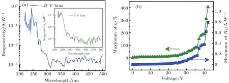


4.Conclusion
猜你喜欢
中国典型病例大全(2022年9期)2022-04-19
华东师范大学学报(自然科学版)(2022年1期)2022-03-29
应用数学(2020年3期)2020-07-28
做人与处世(2018年6期)2018-05-21
祝您健康·文摘版(2018年12期)2018-05-14
中国科技财富(2017年1期)2017-12-23
校园英语·下旬(2017年8期)2017-08-09
创新时代(2017年5期)2017-05-22
南方周末(2016-09-08)2016-09-08
新疆人文地理(2016年3期)2016-05-21

- Chinese Physics B的其它文章
- Entangled multi-knot lattice model of anyon current∗
- Miniature quad-channel spin-exchange relaxation-free magnetometer for magnetoencephalography∗
- Observing the steady-state visual evoked potentials with a compact quad-channel spin exchange relaxation-free magnetometer∗
- Quantum interferometry via a coherent state mixed with a squeezed number state∗
- Cavity enhanced measurement of trap frequency in an optical dipole trap∗
- 7.6-W diode-pumped femtosecond Yb:KGW laser∗