
Epitaxial fabrication of two-dimensional TiTe2 monolayer on Au(111)substratew ith Teasbuffer layer*
2019-05-11 07:30ZhipengSong宋志朋BaoLei雷宝YunCao曹云JingQi戚竞HaoPeng彭浩
Chinese Physics B 2019年5期
Zhipeng Song(宋志朋),Bao Lei(雷宝),Yun Cao(曹云),Jing Qi(戚竞),Hao Peng(彭浩),
Qin Wang(汪琴)1,Li Huang(黄立)1,Hongliang Lu(路红亮)1,‡,Xiao Lin(林晓)1,3,Ye-Liang Wang(王业亮)1,2,Shixuan Du(杜世萱)1,3,and Hong-Jun Gao(高鸿钧)1,3
1Institute of Physicsand University of Chinese Academy of Sciences,Chinese Academy of Sciences,Beijing 100190,China
2School of Information and Electronics,Beijing Institute of Technology,Beijing 100081,China
3CASCenter for Excellence in Topological Quantum Computation,Beijing 100049,China
(Received 3 February 2019;revised manuscript received 5 March 2019;published online4 April 2019)
Keywords:TiTe2,epitaxial fabrication,superlattice,scanning tunneling m icroscopy(STM),low-energy elec
Follow ing the discovery of graphene,tremendous interest in other two-dimensional 2D layered materials has been raised.[1–6]These 2D materials have great potentials in applications of functional devices,[7,8]mainly attributed to their tunable properties w ith various methods,such as through changing the number of layers,chemical components,or by the formation of heterostructures.[1,9]Among thehundreds of 2D materials,transition metal dichalcogenides(TMDs)have drawn much attention recently due to their novel electronic and optoelectronic properties.[7,10]As one member of TMDs,titanium dichalcogenide compounds have been studied extensively,because they show many amazing physical phenomena like charge-density-wave(CDW)state.[11]For example,a real-spaceperiodic latticedistortion in the CDW stateof TiSe2f ilm w ith interstitial Tiatoms wasobserved through the scanning tunneling m icroscope(STM)measurements.[12]Sim ilar phenomenon and possible formation mechanismsabout CDW state in themonolayer TiTe2are also intriguing.[13]Moreover,the spin–orbit coupling or quantum conf inement effects may be observed in these 2D TMDs,these novel phenomena are normally hard to observe in their bulk counterparts.[14–17]A lthough a large number of TMD materials were fabricated in recent years,[3,18–20]new membersof 2D TMD materials family with new structuresarestill desirable,because it holdsnew possibilities for novel physics and device applications.2D TiTe2w ith 1T conf iguration has been fabricated and studied recently,[13,21]but 2D TiTe2w ith 2H conf iguration has not been obtained experimentally so far.
Here,we report the fabrication of 2H-TiTe2monolayer on a Au(111)substrate.The experiments were carried out in an ultrahigh-vacuum(UHV)molecular beam epitaxy(MBE)system w ith a base pressure of about 3×10⁻¹⁰mbar.The Au(111)single crystal surfacewascleaned by cyclesof argonion sputtering and annealing to 760 K until it showed clear diffraction spotsin the low-energy electron diffraction(LEED)pattern and atom ically clean surface in the STM images.The atom ic beams of Te and Ti were evaporated to the asprepared Au(111)substrate from a Knudsen effusion cell and an electron-beam evaporator,respectively.The process for the fabrication of the TiTe2f ilm was as follows:Tewas deposited at f irst,while the substrate was maintained at 573 K,then Ti was deposited at the same substrate temperature,and f inally the substrate was kept at 573 K for 20 m in and then slow ly cooled down.By these processes,the TiTe2f ilm formed on the Au(111)surface w ith Te as the buffer layer.The as-grown samples were characterized in-situ by LEED to gain the crys-superlatticewith respectto the Au(111)substrate,whichhas threedifferentorientations.Scanning tunnelingm icroscopy(STM)measurements clearly show three ordered domains consistentwith the LEED patterns.Density functional theory(DFT)calculations further conf irm the formation of2H-TiTe2monolayeron the Au(111)surface with Teasbuffer layer.The fabrication of this2D layered heterostructureexpands2Dmaterialdatabase,whichmay bring new physicalproperties for future applications.tal structureand then transferred to the STM chamber to study the surfacemorphology and detailed geometric properties.
Density functional theory(DFT)calculations were performed using the Vienna ab initio simulation package(VASP).The projector augmented wave(PAW)method was employed and the Perdew–Burke–Ernzernhof(PBE)version of the generalized gradient approximation(GGA)was used.The electronic wave functions were expanded in plane waves with a kinetic energy cutoff of 300 eV.The k-points sampling was 8×3×1,generated automatically with the origin at the Γpoint.The structures were relaxed until the energy and residual force on each atom were smaller than 10-5eV and 0.01 eV/˚A,respectively.The STM simulations were performed using the Tersoff–Hamann approach.
Figure 1(a)shows the LEED pattern of the as-prepared sample,and the outer six diffraction spots highlighted by the white circles are originated from the hexagonal lattice of the Au(111)substrate.Apart from these spots,the other diffraction spots can be assigned to the well-ordered f ilm.For more clarity,wesketched adiffraction pattern in reciprocal spaceas shown in Fig.1(b),wheregroupsof spotsin differentsizesand colors are classif ied in order to describe different structures and domains.Specif ically,the diffraction spots are divided to two groups,as shown in Figs.1(c)and 1(d).Each group of spots isgenerated by three domainsas represented in different colors.
Figures 1(e)and 1(f)show the lattice structures in real space,corresponding to the diffraction spots indicated by the arrowsin Figs.1(c)and 1(d),respectively.The crystallinematrix of the superstructure in Fig.1(e)is(1,-1|2,3).This sketch distinctly shows a commensurate relation between the f ilm and the substrate lattice,which has a superstructure of.As discussed in the follow ing,this structure can be attributed to TiTe2layer on Au(111)substrate with Te as the buffer layer.
The diffraction spots shown in Fig.1(d)are generated by a high-order commensurate structure of(7/4,1|-3/4,1),as shown in Fig.1(f).They are probably originated from the Te thin f ilm,because excess Te was deposited in the grow th process.The lattice period of this structure in real space is~0.44nm,which isconsistentwith the latticeconstantof bulk Te.The crystal unit cell has a little distortion to be commensurate with the substrate lattice.
To further investigate the surface structure of the sample,STM was used to characterize the surface morphology in real space.Figure2(a)showsan STM imageof thesamplesurface,in which threedomainscan beclearly distinguished,as labeled byα,β,andγ.We can also see that the crystal directions are 30°,-30°,and 90°.To characterize thesurfacestructuremore clearly,we mapped these three domains separately in detail,as demonstrated in Figs.2(b)–2(d).It is clear that the superstructure is an oblique structure.The unit cell of the superstructure ismarked by ablack parallelogram,corresponding tosuperlattice with respect to the Au(111)substrate,consistent with the LEED patterns.
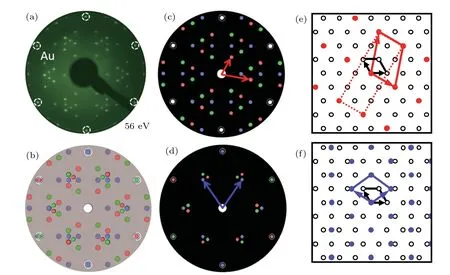
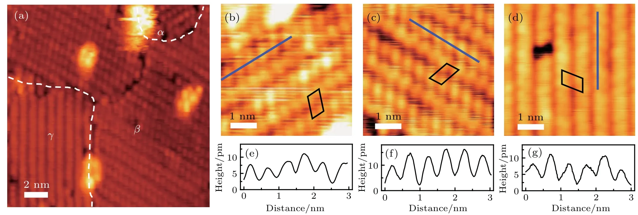
Fig. 2. STM images of t he 2D Ti Te2 l ayer f or med on t he Au(111) sur f ace. (a) STM i mage showi ng t he t hr ee domains, mar ked as a, b, and g. (b)–(d)Zoom-in STM images of t he a, b, and g domai ns in (a). (e)–(g) Line pr of i l es of t he pur pl e l ines in (b)–(d), r espect ivel y, which show per iods of 5.0 A° ,in agr eement wi t h■3 t imes of t he Au subst r at e l at t ice const ant. The sampl e bias and t unnel ing cur r ent: -10 mV, 40 pA i n (a), -0.5 V, 50 p A in (b),-50 mV, 40 pA i n (c) and (d).
Figures 2(e)–2(g)are the line prof iles along the purple linesin Figs.2(b)–2(d),in which theperiod of thesuperstructure is about 5.0˚A,in agreement with■
3 times of the Au substrate lattice constant■.These STM images match with the diffraction spots in the LEED pattern with thestructure.The superstructure in Fig.1(f)deduced from thecomplicated LEEDpattern wasnotobserved in the STM experiments,possibly because STM is a surfacesensitive technique,hard to detect the superstructure underneath thesurfacelayer.
To understand the STM images,we performed DFTbased calculations and simulations.Figure 3(a)shows a stable structure obtained by the calculations.This is a 2H-TiTe2monolayer on the Au(111)surface with a buffer Te layer between the TiTe2f ilmand thesubstrate,which showsa(■3×5)superstructure(red rectangle).Thelatticeconstantsof this2HTiTe2areabout a=3.69˚A and b=3.28˚A,alittlesmaller than that of freestanding 1T-TiTe2of 3.76˚A,[22]which may be induced by the substrate.In order to accommodate the in-plane compression of the lattice constants,the distance between Te atomic layers in the TiTe2sandwich structure is elongated in the z direction to be 4.13˚A,while this distance in freestanding 1T-TiTe2is only 3.47˚A.[22]Figure 3(b)is the simulated STM image of thisrelaxed structure.Besides(■3×5)superstructure(red rectangle),structure(black parallelogram)is also displayed,because the electronic states of the top Teatomsmerge.Figure3(c)isan experimentally obtained high resolution STM image,which shows a good agreement with the simulated result in Fig.3(b),indicating the validity of the structural model with 2H-TiTe2monolayer on Au(111)and Te as buffer layer.We also calculated the structure with 1T-TiTe2asthetop layer and simulated the STM image.However,the results are inconsistent with the■superstructure observed in the LEED and STM experiments.
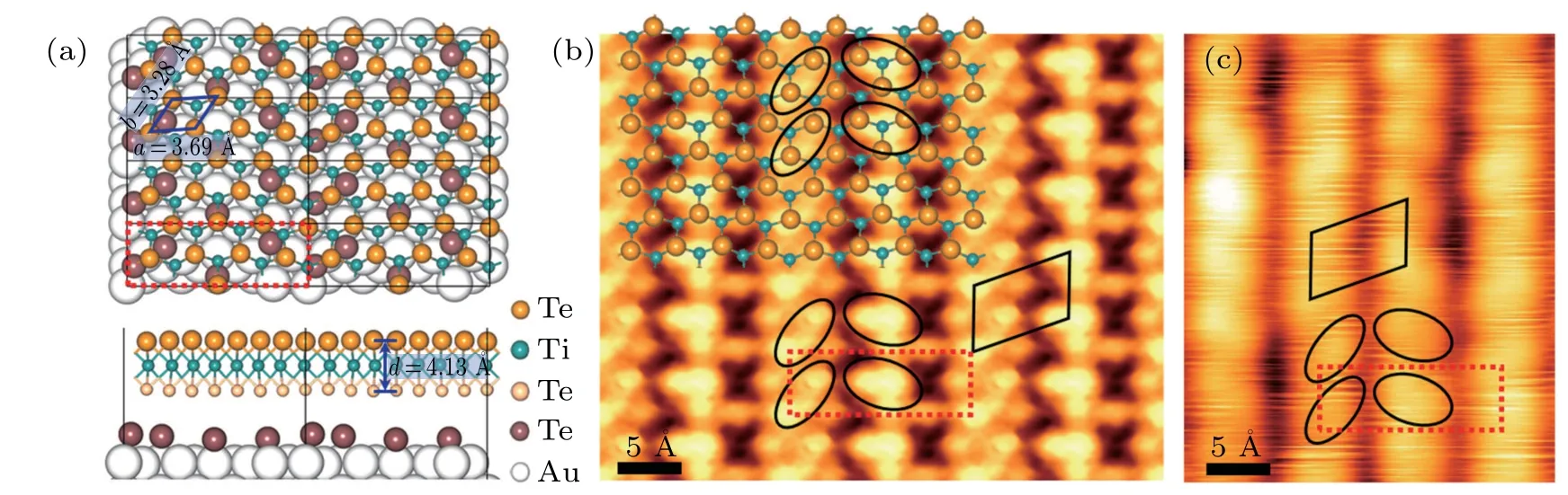
Fig. 3. (a) Top and side views of the relaxed atomic model of the TiTe2/Te/Au(111) structure showing a (■3×5) superstructure (red rectangle).(b) Simulated STM image of the configuration in (a), showing both (■3×5) (red rectangle) and (■3×■7) (black parallelogram)superstructures. The atomic model is overlapped on the top for comparison. (c) High resolution STM image (-50 mV, 40pA ) showing two superstructures.
In summary,we have successfully synthesized 2D TiTe2layer with 2H conf iguration,which is a new member of the TMDs family,on a Au(111)surface by MBE method.STM and LEED characterizations combined with DFT calculations
demonstrate the formation of■superlattice of the TiTe2monolayer with Te as buffer layer on the Au(111)substrate.Thiswork may help to enrich theunderstanding of the superstructures of 2D layered materials and provides a newcandidate in 2D materials family to explore novel physical propertiesand related applications.
- Chinese Physics B的其它文章
- Photoinduced phase transitions in two-dimensional charge-density-wave1T-TaS2*
- Low-tem perature grow th of large-scale,single-crystallinegrapheneon Ir(111)*
- Isotopeeffectand Coriolis coup ling effect for the Li+H(D)Cl→LiCl+H(D)reaction*
- V ariationaland diffusion M onte Carlo simulationsof a hydrogen molecular ion in a sphericalbox*
- General way to def ine tunneling time*
- Dynam icsof two levitated nanospheresnonlinearly coup ling with non-M arkovian environment*