
A High Gain, Noise Cancelling 3.1-10.6 GHz CMOS LNA for UWB Application
2019-07-18 01:59XiaorongZhaoHongjinZhuPeizhongShiChunpengGeXiufangQianHonghuiFanandZhongjunFu
Computers Materials&Continua 2019年7期
Xiaorong Zhao, Hongjin Zhu, Peizhong Shi, Chunpeng Ge, Xiufang Qian, , Honghui Fan and Zhongjun Fu
Abstract: With the rapid development of ultra-wideband communications, the design requirements of CMOS radio frequency integrated circuits have become increasingly high.Ultra-wideband (UWB) low noise amplifiers are a key component of the receiver front end.The paper designs a high power gain (S21) and low noise figure (NF) common gate (CG) CMOS UWB low noise amplifier (LNA) with an operating frequency range between 3.1 GHz and 10.6 GHz.The circuit is designed by TSMC 0.13 μm RF CMOS technology.In order to achieve high gain and flat gain as well as low noise figure, the circuit uses many technologies.To improve the input impedance matching at low frequencies, the circuit uses the proposed T-match input network.To decrease the total dissipation, the circuit employs current reused technique.The circuit uses he noise cancelling technique to decreases the NF.The simulation results show a flat S21>20.81 dB, the reverse isolation (S12) less than -48.929 dB, NF less than 2.617 dB, the minimum noise figure (NFmin)=1.721 dB, the input return loss (S11) and output return loss (S22) are both less than -14.933 dB over the frequency range of 3.1 GHz to 10.6 GHz.The proposed UWB LNA consumes 1.548 mW without buffer from a 1.2 V power supply.
Keywords: Common-gate, low noise amplifier, current reuse, noise cancelling.
1 Introduction
The Federal Communication Commission (FCC) has approved 3.1-10.6 GHz bandwidth for commercial use in 2002, due to its low power consumption, fast transmission speed and high security [Rastegar, Saryazdi and Hakimi (2013); Lin, Hsu, Jin et al.(2007)].The UWB technology is becoming more and more popular because of its low power consumption, high confidentiality, strong penetrating ability and low radiation [Kao and Chang (2008)].
The increasing demands for portable wireless devices are driving the development of CMOS Radio Frequency Integrated Circuits (RFICs) that require low power dissipation to maximize battery lifetime [Rastegar, Saryazdi and Hakimi (2013)].The LNA is the first stage of all UWB front-end RF receivers.Its main function is to suppress noise and amplify useful signals.These two indicators are the key factors of the whole receiver, so the performance of a low noise amplifier directly affects the performance of the entire receiver [Wang, Dinh and Teng (2014)].There are many things to consider when designing an UWB LNA, such as a high enough and flat gain, as low as possible and flat noise figure, good input and output return loss, low power consumption and other requirements over the entire operating frequency range of the UWB LNA.The LNA usually affects the NF and bandwidth in the receiver.Since many indicators cannot be optimal at the same time when designing the LNA, there is a trade-off between gain, noise and bandwidth [Wang, Hwang, Yan et al.(2011)].

Figure 1: Proposed low power, noise canceling schematic
Impedance and noise matching is very challenging in the design of ultra-wideband LNAs today, and will also be crucial for UWB systems [Lo and Kiang (2011)].In designing UWB systems, researchers have proposed many CMOS technologies and topologies for broadband LNA designs such as distributed amplifiers [Zhang and Kinget (2006); Heydari (2007)], resistive shunt feedback [Reiha and Long (2007)], cascade amplifiers [KeHou, JianHao, BoJiun et al.(2007)], and current reused amplifiers [Lin, Hsu, Jin et al.(2007); Khurram and Hasan (2011)].Distributed amplifiers can improve gain at higher frequencies, thus extending bandwidth.But it requires more inductors, so the amplifier is designed to be costly and consumes a lot of power, which limits its range of use.Although the resistor shunt feedback amplifier can provide good input matching, high gain and wideband performance.However, the parasitic capacitance can cause performance degradation when the amplifier is operating at high frequencies [Jung, Yun, Choi et al.(2007); Chen, Lee, Lin et al.(2008)].The current reused techniques are very useful for high gain and low power consumption of the amplifier.However, since current reused techniques requires the use of multiple transistors, it also increases the need for supply voltage, so it is not suitable for low supply voltage conditions [Khurram and Hasan (2011)].
The input stage design of the UWB LNA is critical for forward gain, input matching, and low noise performance.Well-known common source (CS) and CG topologies are widely used by designers for UWB LNA input stages [Khurram and Hasan (2011); Zhang, Fan and Sinencio (2009); Ponton, Palestri, Esseni et al.(2009)].
In recent years, CG LNAs have become more and more widely used in the application of UWB receiving systems because CG LNAs can more easily achieve wider bandwidth, lower power consumption, better linearity and reverse isolation than CS LNAs [Liao and Liu (2007); Zhao, Fan, Fu et al.(2015)].However, the channel noise and gain performance of UWB LNAs are poor due to restrict the value of the transconductance when the input matching is designed [Zhao, Fan, Fu et al.(2015)].
In this paper, we design a UWB LNA with high gain, low noise and low power consumption.Section 2 discusses circuit design and analysis, Section 3 discusses analytical and circuit simulation results, describes the simulation results and compares its performance with other recently published paper.
2 Circuit design and analysis
Fig.1 shows the overall circuit diagram of the proposed UWB LNA.We present a UWB CG LNA architecture in Fig.2, that uses a new T-match input matching network (IMN) consisting of a series Ls-Rs, interconnection-line inductor L1, and Cgs-gm1of transistor M1.Such a structure can improve the input matching of ultra-wideband LNA [Chang and Lin (2011)].The proposed a UWB CG LNA adopt the current reused technique to reduce power dissipation, further eliminating noise in the first stage through noise cancellation technique.
2.1 Input impedance matching network
Input impedance matching is crucial for LNAs as well as the entire UWB system.The input matching circuit design is avoided to use resistors directly, because resistors will dissipate power.The traditional CG LNA is designed to use the inductor Lsto resonates with the gatesource parasitic capacitance Cgsof the transistor M1, ultimately extending the bandwidth of the input match [Cen and Song (2014)].In Fig.2(a), the input impedance of the traditional CG topology can be calculated by the following formula [Cen and Song (2014)]:

where gm1is the transconductance of M1 and r0is the channel resistance of M1.Under the matching conditions, if the channel length modulation and bulk effects are ignored, the input impedance is estimated as [Cen and Song (2014)]:

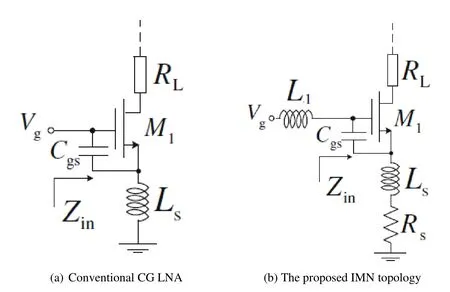
Figure 2: CG LNA Topology
When designing a CG LNA, the value of gm1 must be fixed at 20 mS to achieve 50 Ω input matching.However, impedance matching design is critical and a challenging task in a UWB application.When the gm1value is not equal to 20 mS, the input impedance cannot match the source impedance.In deep-submicron CMOS technology, gm1r0rarely exceeds 10, so RL/gm1r0is roughly equivalent 1/gm1or even exceed 1/gm1[Cen and Song (2014)].In addition, the voltage gain of CG LNA is proportional to gm, and the noise factor is inversely proportional to gm[Cen and Song (2014); Khurram and Hasan (2011)].Therefore, in Fig.2(b) we try to mitigate the limited value of gmby a simple IMN topology.The small signal equivalent model of Fig.2(b) is shown in Fig.3.In Fig.2(b), we propose a CG LNA architecture that uses an input matching network consisting of a series connected Ls-Rs, interconnection inductor L1, and Cgs-gm1of transistor M1, which can improve the input matching for UWB LNAs.In addition, the self-body bias technique used in this design can further reduce the power dissipation of the entire circuit [Chang and Lin (2011)].

Figure 3: Small signal transformation
The input impedance of the circuit from the source of the transistor M1 can be calculated by Eq.(3):


It can be seen that the value of gm1is no longer limited due to Rpis added the circuit, which adds a certain degree of freedom to the circuit in designing the input match.Eq.(4) show that if the circuit achieves 50 Ω input match by adjusting the resistor Rs, then the value of gm1 is no longer limited to 20 mS.We noticed that there is a small DC voltage drop on Rs.Although Rsconsumes a little bit of power, the input matching design can be better realized.Due to the addition of T-matching network, the LNA achieves good isolation and good input match and improves noise performance in the 3.1 GHz to 10.6 GHz band.
Common CG amplifiers must set to gm1=20 mS which can make the circuit to achieve broadband input matching.We try to add a simple IMN to the circuit, so there is no need to fix the value of gm1.The simple IMN as shown in Fig.2(b).
2.2 Noise analysis and noise cancelling technique
In recent years, noise cancellation techniques used in the literature all require the addition of noise cancellation circuits, the designed LNA consumes a lot of power, so this noise cancellation technique is not suitable for portable communication applications.NF is one of the most important parameters to evaluate the radio performance of communication system [Ming, Hongbin, Lianke et al.(2018)].
The total NF of LNA is dominated by the NF of the M1 in Fig.1, so the noise of M1 will be cancelled by the cancelling technology.The principle of noise cancellation technology is that noise generates noise signals with opposite phase polarities in different paths, and then eliminates noise at the output by superposition of opposite phase noises.According to Fig.1, the phase of the noise voltage at point A and the phase of point B are reversed.The noise and signal voltage at node A will be amplified and the voltage phase will be inverted after passing through M2.The signal from the drain of M1 reaches the gate of M2 through Lgand Cg.The phase of the noise and the signal voltage at node C will not change after passing through M3.The noise and signal voltage at node B will be amplified and the voltage phase will be inverted after passing through M4 in a common source configuration.The noise voltages at node E and F will be out-of-phase, the signal voltages at node E and F will be same phase.When Rs, Ls, La, gm2, gm3, and gm4select a specific value, through the noise cancellation technology, M1 current noise will be completely offset.On the other hand, the signal voltages at node E and F in the same phases, the signal voltages are added together at node G.
2.3 Current reused techniques
In order to achieve low power design of low noise amplifiers, this design uses current multiplexing technology to effectively reduce the power consumption of low noise amplifiers.

Figure 4: Current reused architectures
In Fig.4, both (a) and (b) can achieve the desired signal/noise phase difference at input, without adding additional components and contributing to noise cancellation, but due to Fig.4(b) the NF of pMOS is relatively large, so Fig.4(a) is selected.The circuit employs CG nMOS and CS nMOS amplifiers to reduce amplifier power consumption using current reuse techniques.Ultra-wideband and low power consumption are realized by CG LNA, and high gain is achieved by CS LNA.Therefore, the ultra-wideband, high-gain and low-power LNA designed is realized by cascading CG and CS structures.
Conventionally, UWB LNAs with noise cancellation have been designed through cascaded topology connections of M1 and M2.The CG stage (M1) is used to broaden the bandwidth and input impedance matching of the circuit, and the gain is provided to the circuit through the CS stage (M2).In Fig.4(a).By cascading M1 and M2, the same current can supply power to both transistors for the purpose of reducing circuit power consumption.
In the Fig.4, Transistor (M2) reduces power consumption by using a current reused structure.Inductor La is added in the circuit, which not only can improve S11and the S21can be increased.Through the inductor Lgand capacitor Cgseries resonance to achieve bandwidth expansion.LLcan improve the gain flatness through choosing suitable value of LL.
2.4 Stability
The stability of the circuit is an important parameter when designing the LNA.If the LNA is designed to be unstable, it will cause oscillations in the extreme case of voltage changes and may oscillate at unexpected high or low frequencies.The stability factor K is calculated by the following formula.
As per Stern stability analysis, when the stability factor (K) is>1, S11<1, S22<1 and Δ < 1 over the full frequency band, the LNA is unconditional stability.
3 Analytical and circuit simulation results
The simulation results of the proposed LNA are shown in Figs.5-8.which is simulated with Agilent Advanced Design System (ADS) tools.Fig.5 shows the simulated S21and S12against frequency characteristics of the CMOS UWB LNA.High and flat S21of 22.297±1.487 dB, and good S12less than -48.929 dB.As shown in Fig.6, the S11<-14.933 dB and S22<-16.151 dB in the frequency range of 3.1-10.6 dB.Fig.7 shows the simulated of NF and frequency of the designed CMOS UWB LNA.Low and flat NF of 2.169±0.448 dB.Fig.8 shows the simulated stability factor (K) more than 1, so the proposed LNA is unconditional stability over the full frequency band.When the entire circuit is powered by a 1.2 V supply, the circuit consumes 1.548 mW without buffer and 9.6 mW for the entire circuit with buffer.

Figure 5: Simulated S21 and S12 against frequency characteristics
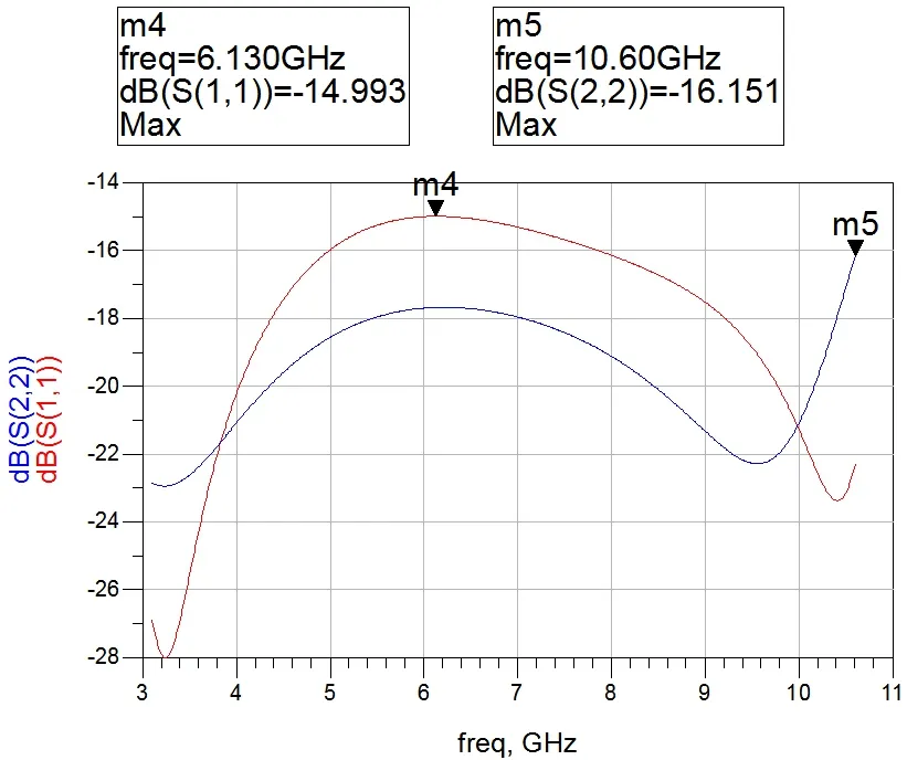
Figure 6: Simulated S11 and S22 against frequency characteristics
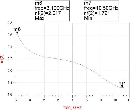
Figure 7: Simulated NF against frequency characteristics
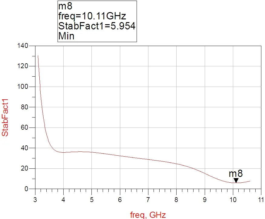
Figure 8: Simulated stability factor against frequency characteristics
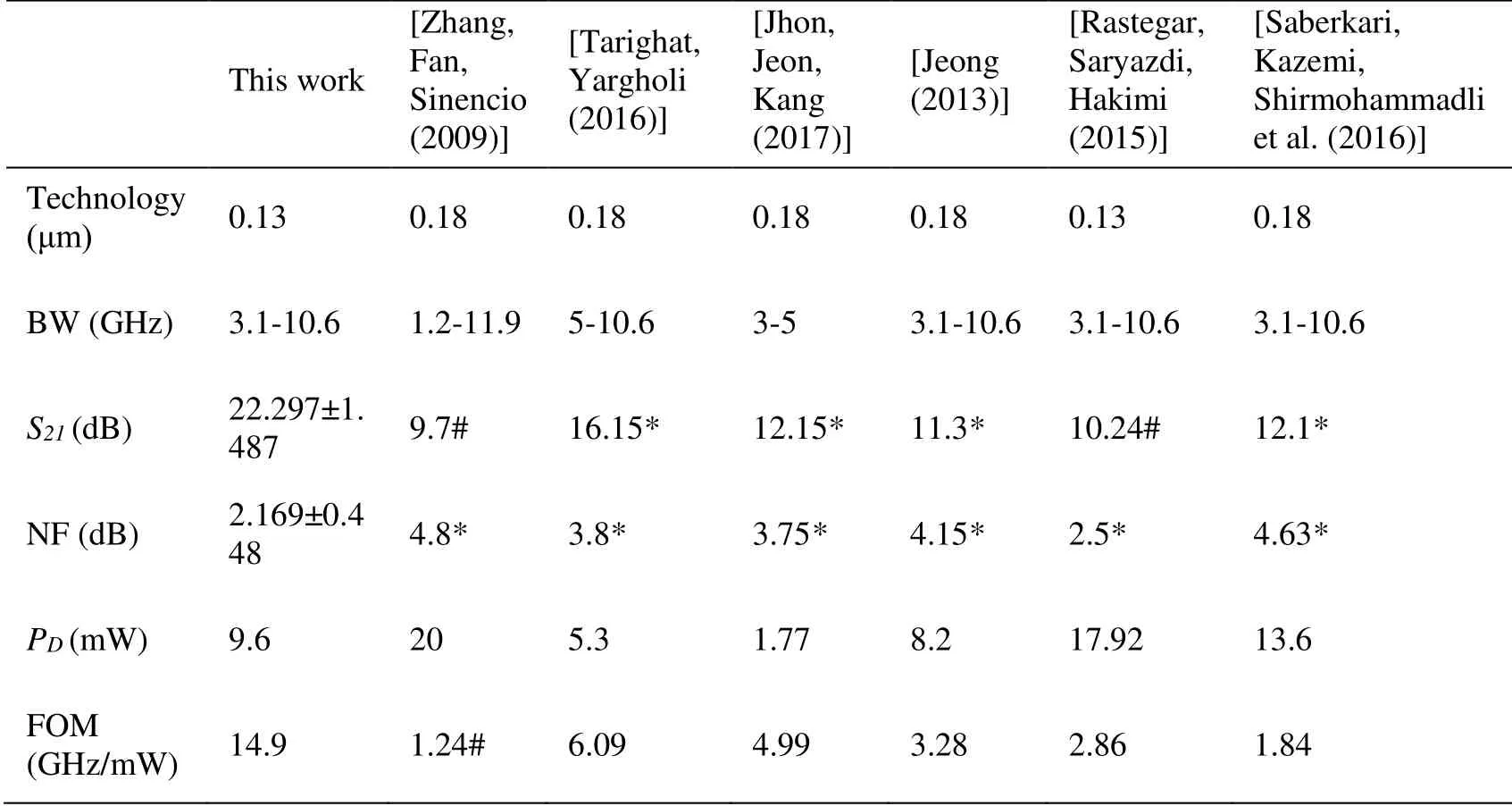
Table 1: Compare with simulation results of lna from other recently published papers
Tab.1 summarizes the performance of other recently published LNAs, which shows that the proposed LNA can obtain high gain and low NF.The proposed UWB LNA exhibits higher FOM compared to other LNAs.The FOM is defined as:

In Eq.(6), |S21| represents the average power gain; BW represents the bandwidth in GHz, |NF| represents the average noise figure; and PDrepresents the power consumption in milliwatts (mW) [Zhao, Fan, Fu et al.(2015); Arshad, Ramzan, Muhammad et al.(2015)].Compared to the low noise amplifier design in most recently published articles, the FOM of the proposed UWB LNA has reached a fairly high level.According to Tab.1, it can be concluded that the designed UWB LNA can achieve a sufficiently high and flat gain, sufficiently low and flat noise and low power consumption.
4 Conclusion
The paper designs a low power and high gain 3.1-10.6 GHz CMOS UWB CG LNA, which uses T-match network technology to improve input impedance matching, current reused technique to reduce power consumption, and noise cancellation technique to effectively reduce input noise.The proposed circuit was designed using TSMC 0.13 μm RF CMOS technology.The simulation results show a high and flat gain of 22.297±1.487 dB, a low and flat NF of 2.169±0.448 dB, S21less than -48.929 dB, S11less than -14.933 dB and output S22less than -16.151 dB, the stability factor more than 5.954 in the frequency range of 3.1-10.6 GHz, the LNA consumes 1.548 mW without buffer from a 1.2 V power supply.In the design of the LNA, good noise figure and maximum power transfer require significantly different input impedance requirements.The current reused technique not only effectively reduces power dissipation, but also conduce to elimination of noise.Compared with the noise cancellation techniques proposed in other literatures, the noise cancellation technique proposed in this paper can make a good tradeoff between maximum power and minimum NF.The structure of the UWB LNA proposed in this paper can achieve sufficient gain, sufficient bandwidth, reasonable NF and proper power consumption.Therefore, the method designed in this paper can provide a good choice for the 3.1-10.6 GHz UWB system application.
Acknowledgement:This work was financially supported by the National Natural Science Foundation (Nos.61602216, 61806088), Jiangsu Province Industry-University-Research Cooperation Project (No.BY2018191), Natural Science Fund of Changzhou (CE20175026) and Qing Lan Project of Jiangsu Province.
References
Arshad, S.; Ramzan, R.; Muhammad, K.; Wahab, Q.U.(2015): A sub-10mw, noise cancelling, wideband lna for uwb applications.AEU-International Journal of Electronics and Communications, vol.69, no.1, pp.109-118.
Cen, M.; Song, S.(2014): A high gain, low-power low-noise amplifier for ultrawideband wireless systems.Circuits, Systems, and Signal Processing, vol.33, no.10, pp.3251-3262.
Chang, J.F.; Lin, Y.S.(2011): 0.99 mw 3-10 ghz common-gate cmos uwb lna using tmatch input network and self-body-bias technique.Electronics.Letters, vol.47, no.11, pp.658-659.
Chen, C.C.; Lee, J.H.; Lin, Y.S.; Chen, C.Z.; Huang, G.W.et al.(2008): Low noise-figure p+ aa mesh inductors for cmos rfic application.IEEE Transactions on Electron Devices, vol.55, no.12, pp.3542-3548.
Chen, K.H.; Lu, J.H.; Chen, B.J.; Liu, S.J.(2007): An ultra-wide-band 0.4-10 ghz lna in 0.18 µm cmos.IEEE Transactions on Circuits and Systems, vol.54, no.3, pp.217-221.
Heydari, P.(2007): Design and analysis of a performance-optimized cmos uwb distributed lna.IEEE Journal of Solid-State Circuits, vol.42, no.9, pp.1892-1905.
Kao, H.L.; Chang, K.C.(2008): Very low-power cmos lna for uwb wireless receivers using current-reused topology.Solid State Electronics, vol.52, no.1, pp.86-90.
Liao, C.F.; Liu, S.I.(2007): A broadband noise-canceling cmos lna for 3.1-10.6-ghz uwb receivers.IEEE Journal of Solid-State Circuits, vol.42, no.2, pp.329-339.
Lin, Y.J.; Hsu, S.S.H.; Jin, J.D.; Chan, C.Y.(2007): A 3.1-10.6 ghz ultra-wideband cmos low noise amplifier with current-reused technique.IEEE Microwave and Wireless Components Letters, vol.17, no.3, pp.232-234.
Lo, Y.T.; Kiang, J.F.(2011): Design of wideband lnas using paralled-to-series resonant matching network between common-gate and common-source stages.IEEE Transactions on Microwave Theory and Techniques, vol.59, no.8, pp.2285-2294.
Jeong, J.(2013): Design of low power cmos ultra wide band low noise amplifier using canceling technique.Microelectronics Journal, vol.44, no.9, pp.821-826.
Jhon, H.S.; Jeon, J.; Kang, M.(2017): Extremely low power lna biased with 0.25-v drain-to-source voltage for 3-to-5 ghz uwb-ir application.Microelectronics Journal, vol.61, pp.1-5.
Jung, J.; Yun, T.; Choi, J.; Kim, H.(2007): Wideband and low noise cmos amplifier for uwb receivers.Microware & Optical Technology Letters, vol.49, no.4, pp.749-752.
Khurram, M.; Hasan, S.M.R.(2012): A 3-5 ghz current-reuse gm-boosted cg lna for ultrawideband in 130 nm cmos.IEEE Transactions on Very Large Scale Integration Systems, vol.20, no.3, pp.400-409.
Khurram, M.; Hasan, S.M.R.(2011): Novel analysis and optimization of gm-boosted common-gate uwb lna.Microelectronics Journal, vol.42, no.2, pp.253-264.
Knoblinger, G.(2009): Design of ultra-wideband low-noise amplifiers in 45-nm cmos technology: comparison between planar bulk and soi finfet devices.IEEE Transactions on Circuits & Systems, vol.56, no.5, pp.920-932.
Ming, H.; Hongbin, W.; Lianke, Z.; Pengming, W.; Andrew, J.(2018): Symmetric learning data augmentation model for underwater target noise data expansion.Computers, Materials & Continua, vol.57, no.3, pp.521-532.
Ponton, D.; Palestri, P.; Esseni, D.; Selmi, L.; Tiebout, M.et al.(2015): A broadband low noise amplifier with built-in linearizer in 0.13-μm cmos process.Microelectronics Journal, vol.46, no.8, pp.698-705.
Rastegar, H.; Saryazdi, S.; Hakimi, A.(2013): A low power and high linearity uwb low noise amplifier (lNA) for 3.1-10.6 ghz wireless applications in 0.13 μm cmos process.Microelectronics journal, vol.44, no.3, pp.201-209.
Reiha, M.T.; Long, J.R.(2007): A 1.2 V reactive-feedback 3.1-10.6 ghz low-noise amplifier in 0.13 µm cmos.IEEE Journal of Solid-State Circuits, vol.42, no.5, pp.1023-1033.
Saberkari, A.; Kazemi, S.; Shirmohammadli, V.; Yagoub M.C.E.(2016): Gmboosted flat gain UWB low noise amplifier with active inductor-based input matching network.Integration the VLSI Journal, vol.52, no.C, pp.323-333.
Wang, S.F.; Hwang, Y.S.; Yan, S.C.; Chen, J.J.(2011): A new cmos wideband low noise amplifier with gain control.Integration, the VLSI Journal, vol.44, no.2, pp.136-143.
Tarighat, A.P.; Yargholi, M.(2016): A cmos low noise amplifier with employing noise cancellation and modified derivative superposition technique.Microelectronics Journal, vol.54, pp.116-125.
Wang, X.; Dinh, A.; Teng, D.(2014): A 3-10 ghz ultra wideband receiver lna in 0.13 µm cmos.Circuits Systems & Signal Process, vol.33, no.6, pp.1669-1687.
Zhao, X.R.; Fan, H.H.; Fu, Z.J.; Ye, F.Y.; Chen, J.F.(2015): Gm-boosted flat gain uwb low noise amplifier with noise cancellation.Chemical Engineering Transactions, vol.46, pp.145-150.
Zhang, F.; Kinget, P.R.(2006): Low-power programmable gain cmos distributed lNA.IEEE Journal of Solid-State Circuits, vol.41, no.6, pp.1333-1343.
Zhang, H.; Fan, X.; Sinencio, E.S.(2009): A low-power, linearized, ultra-wideband lNA design technique.IEEE Journal of Solid-State Circuits, vol.44, no.2, pp.320-330.
 Computers Materials&Continua2019年7期
- Computers Materials&Continua的其它文章
- A DPN (Delegated Proof of Node) Mechanism for Secure Data Transmission in IoT Services
- A Hybrid Model for Anomalies Detection in AMI System Combining K-means Clustering and Deep Neural Network
- Topological Characterization of Book Graph and Stacked Book Graph
- Efficient Analysis of Vertical Projection Histogram to Segment Arabic Handwritten Characters
- An Auto-Calibration Approach to Robust and Secure Usage of Accelerometers for Human Motion Analysis in FES Therapies
- Balanced Deep Supervised Hashing