
Topology of triple-point metals∗
2019-08-06 02:05GeorgWinklerSobhitSinghandAlexeySoluyanov
Chinese Physics B 2019年7期
Georg W.Winkler, Sobhit Singh, and Alexey A.Soluyanov
1Microsoft Quantum,Microsoft Station Q,University of California,Santa Barbara,California 93106-6105,USA
2Department of Physics and Astronomy,Rutgers University,Piscataway,New Jersey 08854,USA
3Institute of Physics,University of Zurich,Winterthurerstrasse 190,8057 Zurich,Switzerland
4Department of Physics,St. Petersburg State University,St. Petersburg 199034,Russia
Keywords: topological metals,topological phonons,electronic structure,thermoelectrics
1. Introduction
Materials with non-trivial band structure topology, apart from possible technological applications,provide a test ground for the concepts of fundamental physics theories in relatively cheap condensed matter experiments. For example,the recent discovery of Weyl semimetals in TaAs materials class[1-5]provided materials in which two bands cross linearly at isolated points in momentum space as illustrated in Fig. 1(a), called Weyl points (WPs).[6]These WPs occur close to the Fermi level, and hence the low energy excitations in these metals are described by the Weyl equation of the relativistic quantum field theory, thus allowing for experimental studies of Weyl fermions, examples of which in high-energy physics are still lacking.
Another example of a topological material hosting a quasiparticle analogue of an elementary particle is that of Dirac semimetals.[7-10]These are centrosymmetric nonmagnetic materials that host Dirac points (DPs) - points of linear crossing of two doubly degenerate bands in momentum space,see Fig.1(b). When DPs are located close to the Fermi level, the low energy excitations of the hosting metal are described by the Dirac equation, and thus become direct analogues of Dirac electrons in high-energy theories.
More recently, it was shown that a variety of possible symmetries realized in solids also allow for the existence of topological quasiparticle excitations,which do not have direct analogues in the standard model,[11-19]rendering novel physical behavior to the hosting compounds. Classification and description of possible topologically protected quasiparticles in solids,along with the identification of material candidates,become of major importance for the progress in materials science and technology, as well as condensed matter theory in general.
The subject of this review is the so-called triple-point(TP)fermionic quasiparticle,which appears at the crossing of a singly and a doubly degenerate band, see Fig. 1(c).[20-23]Apart from the TPs, another class of topologically distinct threefold degenerate band crossing exists representing a spin-1 generalization of a Weyl fermion, see Fig. 1(d). While the TPs occur as accidental degeneracies in both symmorphic and non-symmorphic crystal structures,the latter is limited to high symmetry points in certain non-symmorphic space groups,containing symmetries combined of a point group symmetry operation followed by translation by a fraction of the primitive unit cell vector.[17]While the TPs described here can be also found in non-symmorphic space groups,the symmetry conditions for their appearance coincide in such cases with those of symmorphic space groups. The spin-1 fermion is furthermore characterized by a nontrivial Chern number,which is ill defined for the TPs due to the doubly degenerate band. The nontrivial topology of TPs, on the other hand, is manifested by topologically protected nodal lines and a Z2topological classification applicable for pairs of TPs.
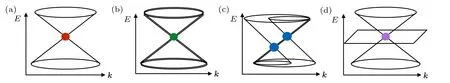
Fig.1. (a)Weyl points are twofold degenerate band crossings of two singly degenerate bands. (b)Dirac points are fourfold degenerate band crossings of two twofold degenerate bands. (c)Triple-points are threefold degenerate band crossings of a singly and a doubly degenerate band.Here a pair is shown. (d)A spin-1 generalization of a Weyl fermion.[17]
2. Classification of triple-points
The realization of a symmorphic TP at a momentum k in the Brillouin zone (BZ) of a crystal structure requires the little group of k to contain both one-and two-dimensional double group representations, since both singly and doubly degenerate bands need to be present for the formation of the TP.Only the point group C3vsatisfies these criteria, thus TPs appear on high-symmetry lines in the BZ with the little group C3v. The elements of C3vare 3-fold rotation C3and 3 mirrors σv, containing the C3axis, rotated by 120°relative to each other.[24-26]One notable exception from this rule is given by space group 174 (C13h), where the interplay of time-reversal and mirror symmetry on a C3-symmetric line also allows for both one-and two-dimensional double group representations.
By using the above symmetry criterion, all space groups that can host TP fermions on a line are identified in Table 1.Note that the little group on the high-symmetry axis of the type-B TP topological metals (TPTMs) is exactly C3v, while for type-A TPTMs it is supplemented by an additional antiunitary symmetry. This symmetry is the product of a mirror plane σhorthogonal to the C3-axis and time-reversal (TR).Its presence preserves the existence of doubly- and singlydegenerate representations, and hence, allows for the existence of TPs. In our consideration, we also included nonsymmorphic space groups,such that the TP crossing includes the same irreducible representations as found in the symmorphic space groups.
The topological classification of TPs into type-A and type-B stems from the different numbers of accompanying nodal lines,and also from the fact that the nodal lines accompanying the two types of TPs are topologically distinct.Due to the three vertical mirror planes, the Berry phase φBaccumulated by valence bands on any mirror-symmetric path(shown in grey in Figs. 2(c) and 2(d)) enclosing the corresponding nodal line is quantized to be either 0 or π.[27,28]The nodal line of type-A TPTMs has φB=0,while all the lines of type-B TPs have φB=π.

Table 1. Space groups allowing for TPs of different types with time-reversal symmetry. The points can appear on high-symmetry lines in the Brillouin zone:Δ=(0,0,α),Λ=(α,α,α),P=(-1/3,2/3,α)(hexagonal lattice),P=(1/2-α,1/2-α,-1/2-α)(rhombohedral lattice),and F =(1/4+α,1/4-3α,1/4+α). Triple-points appear in trigonal,hexagonal,and cubic space groups. Note that the table also contains non-symmorphic space groups but the TPs exist on lines where the non-symmorphicity does not change the irreducible representations, thus they are identical to the TPs found in the symmorphic space groups. The case of the non-symmorphic space group 220 has also been treated in Ref.[17]. We note that,in addition,the groups 162-167,191-194,and 221-230 admit type-B TPs provided that time-reversal symmetry is broken in a way preserving C3v representations on a line in the Brillouin zone.
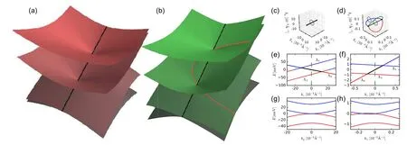
Fig. 2. Two types of fermionic triple-point quasiparticles. (a) and (c) Type-A triple-points are connected by a single nodal line, where conduction and valence bands are degenerate (shown in black). (b) and (d) Type-B triple-points are accompanied by four such nodal lines,shown in black, green, blue, and red. The latter three occur in the mirror-symmetric planes in momentum space. The grey circles in (c)and (d) indicate paths for the Berry phase calculation. (e) and (f) Band structures around type-A and type-B triple-points along the C3 axis,respectively. Here Λ6 represents the double degenerate band (double representation of C3v), while Λ4,5 correspond to two one-dimensional representations. The black lines in(e)and(f)mark the region of the band structure that produces the nodal lines shown in black in panels(c)and (d). (g) and (h) Band structures around type-A and type-B triple-points in a mirror symmetric plane orthogonal to kz, respectively. The dashed green lines in(e)and(f)mark the momentum kz used in panels(g)and(h). Red(blue)color in panels(e)-(h)corresponds to occupied(unoccupied)bands assuming that the Fermi level is exactly between the pair of triple-points. Figure partially reused from Ref.[21].
These values are consistent with the band structure plots shown in Figs. 2(e)-2(h). In type-A TPTMs, the crossing of conduction and valence (occupied and unoccupied) bands occurs on a high-symmetry line and is quadratic, while for the type-B phase this quadratic touching point splits into two points, where the bands cross linearly. The presence of nodal lines with nontrivial Berry phase, as is the case for type-B,is generally associated with the appearance of surface states.[28,29]The merging and subsequent annihilation of nodal lines are similar to those of the nexus point discussed in the context of3He-A and Bernal-stacked graphite with neglected spin-orbit coupling(SOC).[30-33]We stress,however,that the scenarios discussed in the present work take full account of SOC.
Analogous to WPs,[6]the minimal number of TPs in the BZ is four for materials preserving time-reversal symmetry. A pair of TPs located on a C3v-symmetric line can be split into four WPs by lowering the C3vsymmetry to C3(breaking σv),which can be achieved by a small Zeeman field parallel to the C3axis or by an atomic distortion. Conversely, imposing inversion symmetry onto the atomic structure makes the two TPs merge into a single DP. Hence, the TPTMs can be viewed as an intermediate phase separating Dirac and Weyl semimetals in materials with a C3v-symmetric line in the BZ.
3. Triple-point materials
The possibility of new fermions in condensed matter systems sparked a huge effort in the first-principles community to look for suitable material candidates. While band structures with threefold degenerate crossings appear to be comparatively rare in nature, using extensive scans of material databases enabled by high-throughput calculations, a decent amount of material candidates for TPTMs could still be identified. Experimental investigations of some of these materials are currently under way with some results already published.[34-38]In Table 2,we list all TPTMs that have been predicted by first-principles methods up to the point of this writing.
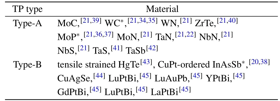
Table 2. Theoretically predicted TPTMs classified in type-A and type-B. Material candidates for which experimental evidence of TPs exists are marked by an asterisk.
The TPTMs have been predicted in three types of crystal structures: type-A TPTMs are exclusively of a tungsten carbide (WC) structure and type-B TPTMs either have cubic symmetry (HgTe, half-Heuslers) or are obtained by breaking the cubic Tdsymmetry to the subgroup C3v(tensile strained HgTe,CuPt-ordered InAsSb).
3.1. Triple-points in tungsten carbide like crystal structure
The type-A TPTM phase has been identified in a family of two-element metals AB(A={Zr,Nb,Mo,Ta,W},B={C,N,P,S,Te,Sb})listed in the type-A row of Table 2.These materials have a WC-type structure that belongs to space group P¯6m2 (D13h=187). The primitive unit cell, shown in Fig.3(a),consists of two atoms A and B at Wyckoff positions 1a (0,0,0) and 1d (1/3,2/3,1/2), respectively. The corresponding bulk BZ is shown in Fig. 3(b) along with the (001)and(010)surface BZs.
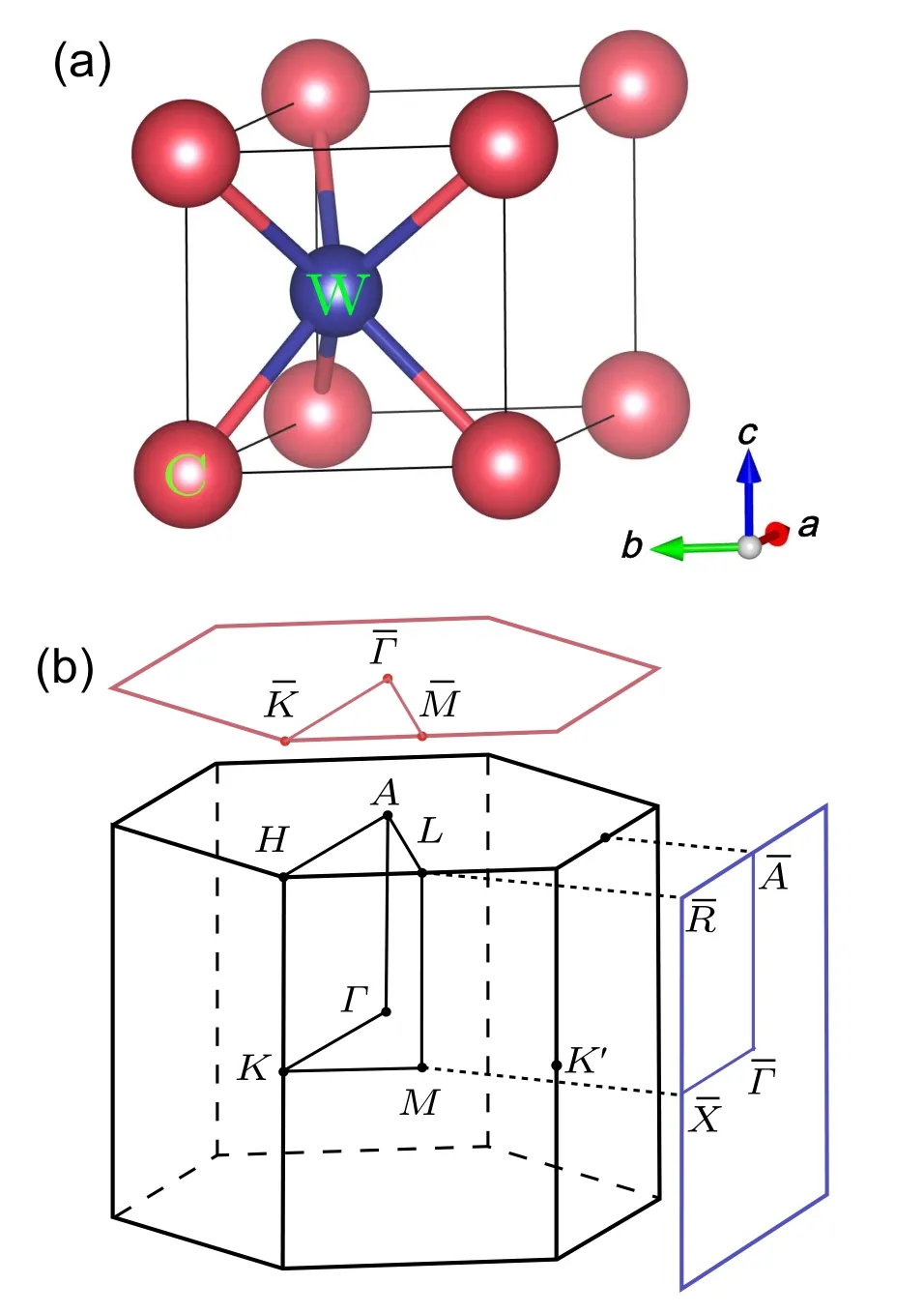
Fig. 3. (a) Primitive unit cell of WC-type structure. (b) The bulk BZ and(001)and(010)surface BZs. Figure reused from Ref.[21].
Now we discuss the band structure obtained by ab initio simulations.[21]Figure 4 shows the band structures of ZrTe,WC,and TaN,which will be used as representative materials.
In the absence of SOC,there is a band inversion at K and K′points in ZrTe and WC(Figs.4(a)and 4(c)),resulting in a nodal ring in the kz=0 plane protected by σh,while this band inversion is absent in TaN.The common feature of all materials is that along the C3v-symmetric Γ-A line, there is a band crossing of the singly and doubly degenerate bands due to the pounds. Topological confirmation of the presence of band inversion is given by the non-trivial values of the mirror Chern numbers[46]on the σhplanes,see Fig.5,which are C±i=∓1,for the mirror eigenvalues±i,respectively in the kz=π plane for the materials considered here.[21]In the kz=0 plane,one finds C±i=∓1 for ZrTe,MoP,and NbS and C±i=0 for MoN,TaN,and NbN.The materials MoC,WC,and WN have nodal lines in the kz=0 plane and,therefore,the mirror Chern number is ill defined for them.
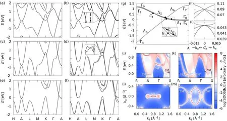
Fig. 4. Band structures of (a) ZrTe, (c) WC, and (e) TaN without SOC. Those with SOC are correspondingly shown in panels (b), (d), and(f). The Fermi energy is set to 0 eV.(g)Band structure of ZrTe along the Γ-A line. Bands are labeled by their double group representations corresponding to D3h at Γ and A points and C3v on the Γ-A line. (h)and(i)Band structures in the(100)direction with kz tuned to the TPs G1 and G2,respectively. (j)and(k)Projected surface density of states(SDOS)for the(010)surface of ZrTe with(j)Zr and(k)Te termination. (l)and(m)The(010)-surface Fermi surface of ZrTe at E=0 eV for(l)Zr and(m)Te termination. Figure reused from Ref.[21].
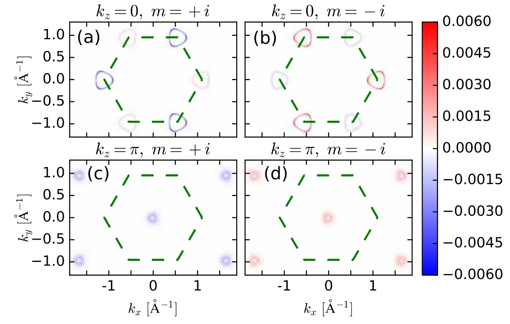
Fig. 5. The Berry curvature for (a)-(d) specific mirror eigenvalues on σhmirror invariant planes in ZrTe. Figure reused from Ref.[21].
In ZrTe,the nodal ring around K and K′points acquires a small gap(see also the inset in Fig.4(b)). Interestingly,three pairs of WPs,slightly away from the kz=0 plane,form at each K and K′point in ZrTe[40]and also in MoP.[36]WC(together with MoC and WN) remains a nodal line metal (see inset of Fig. 4(d)). There exist two nodal rings (one inside another)formed by two touching bands protected by the horizontal mirror σh. For WN,there is only a single such nodal ring around each K and K′. The stability of these topological features has been checked with the HSE06 hybrid functional.[21,47]Furthermore, the band structure of MoP has been recently experimentally investigated using angle-resolved photoemission spectroscopy (ARPES), confirming experimentally the presence of TPs and WPs.[36]
In Fig.4(g),a zoom-in of the Γ-A line in ZrTe is shown.The Fermi level resides in between the Γ9and Γ8bands at A.Upon turning on the SOC,the no-SOC Λ3state splits into the singly degenerate Λ4+Λ5states and the doubly degenerate Λ6state. Another Λ6state comes from the no-SOC Λ1. The two Λ6states hybridize and each of them crosses with the spin-split Λ4,5states, creating 2 pairs of TPs: (G1,G2) and (G3,G4).Each TP is protected by the C3vsymmetry of the Γ-A line.Figures 4(h)and 4(i)show the dispersions in the(100)direction for kztuned to the positions G1and G2, respectively. A linear band crossing superimposed with a quadratic band reinversion of the singly- (Λ1) and the doubly-degenerate (Λ3)states at A. This crossing produces a single no-SOC TP,and it is this feature that generates four TPs upon introducing SOC.
All the considered materials have sizable SOC, which cannot be neglected. Due to the lack of inversion symmetry, the bands are spin-split at generic momenta as shown in Figs. 4(b), 4(d), and 4(f). One finds a band inversion along the H-A-L line such that the A point acquires an inverted gap for all materials. Consequently, the kz=π plane becomes an analogue of a 2D quantum spin Hall insulator in all of the comsembles a WP,degenerate with a quadratic band,similar to the findings of Ref. [20] for type-B TPTMs. Again, band inversion is the mechanism leading to the formation of TPs.
In Figs. 4(j) and 4(k), the surface states of ZrTe for the (010) surface are shown.[21,48]The surface potential is found to depend strongly on the termination choice: Zr (Te)-termination is shown in Fig.4(j)(Fig.4(k)). Since the kz=π plane is a quantum spin Hall insulator plane, a Kramers doublet of surface states should appear along theline of the surface BZ. Consequently, there is a surface Dirac cone SS1 located atfor Zr (Te) termination. The surface states forming the Dirac cone emerge from the TPs G1and G2. For kzvalues below the location of G1and G2,there exists another pair of surface states SS1′emerging from the TPs. SS1′,however,is not topologically protected.
The K′point of the bulk BZ is projected onto theΓ-X line in Figs. 4(j) and 4(k) (compare to Fig. 3(b)). A small gap due to SOC can be visible in the projected bulk spectrum around the projection of K point (shown with an arrow). For ZrTe,the kz=0 mirror plane hosts a quantum spin Hall phase with the mirror Chern numbers ±1, thus one can expect to see a Kramers pair of topological surface states along the lineThis expectation is further supported by the Berry curvature calculation in the kz=0 plane, see Fig.5. It reveals the accumulation of Berry curvature in an area around the K (K′)point that sums up to approximately-1(1).[21]In accord with this topological arguments, one finds a quantum Hall like surface state SS2 crossing the gap alongΓX (its Kramers partner is not shown,being at TR-symmetric part of the surface BZ.
Figures 4(l) and 4(m) show the (010)-surface Fermi surface revealing double Fermi arcs between the two hole pockets containing the TPs,corresponding to SS1 and SS1′. The state SS2 is not visible for this choice of the Fermi level. For the Te termination, the Fermi arcs connect the two hole pockets,while they do not touch the hole pockets for the Zr termination.In both cases,however,the surface states are protected by TR and mirror symmetry on the kz=π plane, so they cannot be fully removed from the spectrum. ARPES investigations of the very similar TPTM WC prove the existence of the surface Fermi arcs SS1 and SS1′.[35]
3.2. Cubic symmetry
One of the first account of TPs has been given in the context of HgTe by Saad Zaheer et al. in Ref. [43]. According to the cubic symmetry, there are eight equivalent directions with little group C3vhosting possible TPs. Due to the lack of a horizontal mirror,these TPs are all of type-B.The situation is complicated by the fact that the Λ4,5and Λ6states are degenerate at Γ forming the four-dimensional Γ8representation.This leads generically to eight TPs near a Γ8crossing along the eight equivalent Λ directions, see Fig. 6(a). However, in the HgTe case,the TPs are extremely close to Γ such that they are impossible to resolve with available experimental techniques.
The same scenario takes place in half-Heusler compounds with band inversion.[49]Interestingly,in some compounds like LuPtBi, LuAuPb, and YPtBi, the energy bands have such a strong non-parabolicity that additional TPs appear.[45]The evolution of the band structure with increasing number of TPs is illustrated in Figs. 6(b) and 6(d). Therefore these half-Heusler compounds have three TPs in each equivalent 111 direction, 24 in total. Furthermore, these TPs are well separated from the Γ point with observable Fermi arcs on the easily cleavable(111)surface.[45,50,51]These properties make the half-Heusler compounds ideally suited to experimentally investigate the intricate topology and surface states of type-B TPs.

Fig.6. Energy bands along L-Γ-L in cubic crystals with band inversion. The thick blue line is doubly degenerate whereas black lines are non-degenerate. (a)HgTe-type energy bands.(b)-(d)Evolution of band structure in half-Heusler materials with increasing number of TPs. Illustration adapted with permission from Ref.[45].
3.3. CuPt-ordered InAs1-xSbx
Above we have seen that the TPs of the cubic HgTe are too close to Γ to enable a direct experimental observation.However, this can be changed by applying a moderate tensile strain in the 111 direction, such that the remaining point group is broken down from Tdto C3v.[43]In this case, two pairs of TPs survive. Unfortunately,it is experimentally difficult to apply 111 strain to HgTe. The ingredients to achieve well separated TPs in HgTe are band inversion and breaking of cubic Tdsymmetry to C3v. It is no surprise that the same ideas can be applied in other III-V semiconductors. The difficulty of applying 111 strain can be overcome by changing the mechanism of symmetry breaking from strain to alloy ordering. Fortunately, some ternary III-V compounds show naturally a so-called CuPt-ordering,[52]which is ordering in alternating 111 planes, see Fig. 7(a). This type of ordering provides exactly the desired symmetry breaking. Especially promising is the InAs1-xSbxsystem.[20]InAs and InSb are both small band gap semiconductors and the band gap is further reduced in their alloy.[53-55]CuPt-ordering further reduces the band gap[52,56,57]and first-principles calculations show that the perfectly CuPt-ordered InAs0.5Sb0.5alloy has an inverted band order.[20,58]While perfect atomic CuPt-ordering in InAs0.5Sb0.5is difficult to obtain,the same effect is achieved by growing layered structures of InAs1-xSbxwith alternating alloy composition x. With this approach,the band gap can be tuned from normal to inverted band ordering.[38,59]
The band structure of CuPt-ordered InAs0.5Sb0.5obtained from first-principles simulations is shown in Fig. 7(b).[20]A pair of TPs is formed at the crossings of the Λ4,5with the Λ6band. The Λ4,5bands have a very small linear in k, splitting,which is only about 2 meV at the momentum of the TPs. The pair of TPs is thus very close together and will appear like a single Dirac point in low resolution experiments.
Another very interesting aspect of CuPt-ordered InAs1-xSbxis that the symmetry breaking to C3vsimultaneously allows for a Rashba-type spin-orbit splitting in the conduction band, provided that the band order is normal.Either by imperfect CuPt-ordering, or by 111 strain, the normal band order can be restored and one obtains a giant-Rashba material, see Fig. 7(c). Large Rashba splitting is a crucial ingredient for topological quantum computers relying on non-abelian Majorana,[60-64]quasiparticles realized in semiconductor nanowires.[65,66]Since InAs and InSb are the preferred materials for the experimental realizations of Majorana quasiparticles,[67-71]CuPt-ordered InAs1-xSbxseems to be a very promising material for this application.[20]
Figures 7(e) and 7(f) show the surface density of states of the(1¯10)surface.[20]In this case, the Fermi arcs resulting from the TPs look very similar to those from the typical Dirac semimetals[7,8,10]due to the small separation of the TPs.
Fig.7. (a)Crystal structure of CuPt-ordered InAs0.5Sb0.5. (b)Band structure of CuPt-ordered InAs0.5Sb0.5 around Γ (plotted up to|k|=0.1 ˚A-1). (c)Band structure with 3%compressive strain applied in the 111-direction. (d)Brillouin zone and surface projection of CuPt-ordered InAs0.5Sb0.5. (e) Surface density of states for the (1¯10) surface. (f) Topological Fermi arcs on the (1¯10) surface.Figure partially reused from Ref.[20].
4. Topological properties of the triple-point fermions
In this section,we first introduce simplified models of TP materials and use them to discuss the topological properties of TPs.
4.1. Microscopic models
Before we investigate the topology of TPs, we introduce a few simple k·p-models for type-A and type-B triple-points.
The type-A k·p-models are up to a change of basis identical to the ones in Ref. [21] and the given parameters correspond to the material realization of ZrTe. The type-B k·p-models are also up to a basis transformation identical to the ones in Ref. [20] and the parameters correspond to the CuPt-ordered InAs0.5Sb0.5case.
4.1.1. Type-A: ZrTe
For the WC-class of type-A TPTMs, we construct a model around the A point which captures the band inversion and describes the TPs. We include the Γ9, Γ8, and Γ7states(see Fig.4(g)and Table 65 of Ref.[24])with energies close to the Fermi level. Along the z-axis, the Γ9representation splits into the Λ4,5representations and both Γ7,8become Λ6. The little group of A is D3hplus TR symmetry. For the derivation of the k·p models, we need to identify the correct representations of the symmetry operations. The Hamiltonian is then constructed such that it commutes with all symmetries S

with RSbeing the representation of S in the basis of H. Since all representations are two dimensional, the symmetry representation is the direct sum of two-dimensional representations with τx,τy,and τzbeing the Pauli matrices.

Considering the constraint Eq. (1) for all symmetries above,one obtains the following Hamiltonian:

using the definition εi(k)=Ei+Fi(k2x+k2y)+Gik2zand k relative to the A point. Via fitting to the ZrTe band structure,we obtain the following parameters for Eq.(3):E1=-0.0391 eV,E2= 1.3709 eV, E3= 0.0391 eV, F1= 3.75 eV·˚A2, F2=-0.5 eV·˚A2, F3= 4.25 eV·˚A2, G1= 2.2 eV·˚A2, G2=-12.64 eV·˚A2, G3= 1.5 eV·˚A2, A = 0.17 eV·˚A, B =0.24 eV·˚A, C = 2.9 eV·˚A, D = 0.054 eV·˚A, and E =2.76 eV·˚A.
If the influence of the Γ7state is removed, one obtains a 4×4 model

To simulate the interaction of the two Λ6bands, we add a fourth order term to ε3(k) = E3+F3(k2x+k2y)+G3k2z+H3k4z. We find the following parameters via fitting to the band structure of ZrTe: E1=-0.0391 eV, E3=0.0391 eV,F1=4.5 eV·˚A2, F3=-7.3 eV·˚A2, G1=2.2 eV·˚A2, G3=3.2 eV·˚A2,H1=0 eV·˚A4,H3=-20 eV·˚A4,A=0.17 eV·˚A,and D=0.487 eV·˚A.Note that the parameter A is the only one that breaks inversion symmetry in the above model. Setting A=0,one obtains a k·p description of a Dirac semimetal.
A four-band Hamiltonian in the vicinity of a pair of TPs,where k is understood relative to the midpoint of the two TPs,is given below

R(Γ9)⊕R(Γ7)⊕R(Γ8),
Instead of σhand TR, only their product θ°σhneeds to be taken into account at a general k-point on the C3v-symmetric z-axis. In the following,we use E0=30 meV,A1=1.4 eV·˚A,A2= 0 eV·˚A, B = -1.0 eV·˚A, C = 1.082 eV·˚A, and D =0 eV·˚A. We use the above k·p model for the illustrations of the type-A TPTM in Fig.2.
The WC-class of TPTMs also has interesting topological properties around the K-points.A good k·p description of the topology and bands around K (or K′)requires at least 8 states.The little group of the K points is C3hand the Γ7,Γ12,Γ11,Γ9,Γ12,Γ10,Γ8,and Γ7states(see Table 57 of Ref.[24])are determined to be relevant for constructing a k·p-description. We use the following symmetry representations:
Considering the symmetries given above,the lowest order Hamiltonian around K is given by

using εidefined in Eq. (3), k±=kx±iky, and k relative to K. Since K is not a time-reversal invariant momentum,bands do not form doubly degenerate Kramers pairs at this point.For the k·p model around the K point, we obtain the following parameters (in units of eV and ˚A) via fitting to the ZrTe band structure: E1= -0.0979, E2= -0.0671, E3=0.6538,E4=0.8393,E5=1.0661,E6=1.1351,E7=1.2145,E8=1.2774,F1=F2=3.6,F3=F4=-2.0,F5=F6=6.0,F7=F8=1.5,G1=G2=3.6,G3=G4=-0.2,G5=G6=2.0, G7= G8= -3.0, A1= A′1= 4.0, A2= 0.2, A3= 0,A4=0, B1=0.2-i0.1, B2=0.02-i0.01, B3=0.2, B4=-0.2, B5=-1.0+i4.0, B6=-4.0+i1.0, B7=3.0+i0.5,B8=-0.5+i3.0,and B9=1.5. The Weyl points reported in Ref.[40]are also described by this k·p model.
4.1.2. Type-B: CuPt-ordered InAs0.5Sb0.5
The type-B scenario differs only by the absence of the horizontal mirror σh. For completenes, we give the corresponding representations again, albeit σvis now a mirror in the xz-plane instead of the xy-plane as before. The representations below correspond to a Λ4,5⊕Λ6-basis
Around Γ the following model is obtained:

with the following set of parameters for CuPt-ordered InAs0.5Sb0.5: E1=0.1696 eV,E2=0 eV,F1=-5.86 eV·˚A2,F2= 14.3 eV·˚A2, G1= -3.91 eV·˚A2, G2= 54.2 eV·˚A2,A=0.02 eV·˚A,B1=0,B2=1.48 eV·˚A,and C=1.26 eV·˚A.
Omitting the TR symmetry, a Hamiltonian of a pair of TPs,with k relative to the midpoint of the two TPs,is obtained as

In contrast to Eq. (5), the parameters D and F can now take complex values. We use E0=0.88 meV, A1=-0.42 eV·˚A,A2=0 eV·˚A, B=4.22 eV·˚A,C=0.78 eV·˚A, D=0.755-0.445i,and F=-1.69+0.755i.We use the above k·p model for the illustrations of the type-B TPTM in Fig.2.
4.2. Wilson loop characterization for pairs of triple-points
The tracking of Wilson loop eigenvalues,[72]or equivalently the so-called hybrid Wannier centers,[73]under an adiabatic modification of a Hamiltonian has been proven as an invaluable tool for classifying topological phases.[11,74-76]Here atopological classification based on the Wilson loop is developed for pairs of TPs.
The Wilson loop can be defined on any path in k-space connecting two points k1and k2with the property k1=k2+G, where G is a reciprocal lattice vector. The Wilson loop is defined as the path ordered product[72]
with Pk=∑n∈occ.|un(k)〉〈un(k)| the projector on the occupied subspace of a Hamiltonian.The Wilson loop is inherently gauge invariant due to the gauge invariance of the projector Pk.The Berry phase associated with the loop is given by the determinant of the Wilson operator det(W)=exp(iφB). If the Hamiltonian has a symmetry R,it can be shown that[77]

with R acting in reciprocal space and ˜R in occupied band space. The symmetry expectation value of Wilson loop eigenstates|vi〉is calculated as〈vi|˜R|vi〉.
For Weyl[11]and Dirac[76]semimetals it is known that the Wilson loop spectrum on a sphere enclosing the semimetallic point gives the topological classification of the crossing. Also in our case with TPs, a similar kind of topological classification is possible. Here the classification is demonstrated with a tight-binding model of ZrTe obtained in Ref.[21].
In Fig. 8(a), we show a spherical surface on which the Wilson loop spectrum is to be evaluated. The sphere is chosen such that the Hamiltonian is gapped everywhere on the surface, the symmetry axis containing the TPs goes through the center of the sphere and both TPs are enclosed by the sphere.The latter point is important,since there is always at least one nodal line connecting two TPs, therefore including only one TP would not fulfill the requirement that the Hamiltonian is gapped on the sphere. Note that the Wilson lines are oriented such that the symmetry axis goes through their center.In Fig. 8(c), we plot the phases φiof the individual Wilson loop eigenvalues as a function of the azimuthal angle θ. The tight-binding model has 8 occupied states,therefore,we obtain 8 Wilson loop eigenvalue phases φi. Six φi(marked in black)are trivial and stay very close to 0(2π),but two(marked in red and blue)seem to cross. Note that the σvsymmetry constrains the φisuch that the Wilson loop spectrum is mirror symmetric φi=-φj.[27]Since the Hamiltonian is gapped on the surface,and the Wilson loop is gauge invariant,the individual φichange smoothly with θ. Therefore,the connectivity of the φican be determined as long as they are not degenerate. To obtain the connectivity across the degeneracy point between the red and blue Wilson eigenvalues,we calculate the C3symmetry expectation values of the corresponding states in Fig.8(d).The grey dashed line in Fig.8(d)indicates the position of the crossing of the blue and red lines in Fig. 8(c). Note that the crossing of red and blue lines in Fig.8(d)is accidental and we find that it can be avoided via choosing a cigar-shape, rather than a sphere. However, the C3symmetry expectation value is nondegenerate at the crossing in Fig. 8(c) and we can use Fig.8(d)to unambiguously determine the connectivity for all θ. Therefore, the red and blue lines in the Wilson loop spectrum clearly indicate two hidden Berry curvature fluxes, one inward and one outward, through the sphere. The fluxes can be separated in the Wilson loop eigenbasis, corresponding to individual Chern numbers[78]of ±1. The difference of the two individual Chern numbers divided by two constitutes a Z2topological invariant for the TPs.
At the polar regions θ ≈0 or θ ≈-π, the Wilson loop commutes with the C3symmetry due to Eq.(12). In this case,the C3expectation value in Fig. 8(d) is one of the possible C3eigenvalues {-1,exp(iπ/3),exp(-iπ/3)}, which are the starting and ending points of the lines in Fig. 8(d). Note that the 6 trivial φi(black dots) are almost fixed to the C3eigenvalues, whereas the 2 nontrivial φi(red/blue dots)change the C3eigenvalue from {-1,-1} to {exp(iπ/3),exp(-iπ/3)}.Responsible for this behavior are the two valence bands having the rotational eigenvalues -1,-1 for kzto the left of the two TPs and exp(iπ/3),exp(-iπ/3)for kzto the right of the two TPs. Therefore,the planes above G1,G2are topologically distinct from the planes below, consequently uncovering the existence of crossing points realized as the two TPs here.
In Fig. 8(b), we give an example of a topologically trivial pair of TPs. In this case,the C3eigenvalues of the valence bands are the same to the left and to the right of the two TPs and hence the Wilson loop spectrum is in general gapped with an even Z2invariant.
Fig. 8. (a) Pair of TPs (red points) connected by a nodal line (red line) enclosed by a sphere. The arrows indicate the individual Wilson loops winding around the sphere. (b)Example of a trivial pair of TPs. (c)The Wilson loop spectrum on a sphere enclosing a pair of TPs. Two Wilson loop eigenvalues feature gapless flows(colored in red and blue). (d)The C3 symmetry expectation value of individual Wilson lines. Figure reused from Ref.[21].
4.3. Lifshiftz transitions
Using the models of Eqs. (5) and (10), we can analyze the Lifshitz transitions of Fermi surfaces in the TPTMs. The nodal lines of Figs.2(a)and 2(b)guarantee that several Fermi surfaces touch within a finite energy window in between two TPs. Figure 9(a)illustrates the fixed ky=0 cuts of the Fermi surface for the Fermi level EFplaced above,below,and in between the two TPs, representing three topologically distinct Fermi surfaces. At each of the two TPs,a topological Lifshitz transition takes place: one of the Fermi pockets shrinks to a point reopening either inside or outside another Fermi pocket.When EFis placed in between the two TPs, there appears a topologically protected touching point between electron and hole pockets,similar to the type-II WP scenario.[11]
The Lifshitz transitions occurring in type-B TPTMs are illustrated in Fig.9(b).The difference to the type-A transitions is that a single touching point between the Fermi pockets(the point of quadratic band touching) now splits into four points(or two linear band touchings on each mirror plane)due to the breaking of σh(see insets of Fig.9(b)). Intricate spin textures with changing winding numbers were predicted for a (111)-strained HgTe in Ref.[43],which according to the classification is a type-B TPTM.Nontrivial windings in the spin-texture are also found for type-A TPTMs.[22]
Since the distinct Fermi pockets touch in TPTMs for a range of energies,the topological charge of individual pockets is undefined.However,as mentioned above,this degeneracy is lifted via breaking σvby, for example, applying a small Zeeman field in the z direction or photoirradiation effects.[79]In this case, each of the TPs splits into two WPs with opposite Chern numbers as illustrated in Fig.9(c). The touching Fermi pockets now separate,and well-defined Chern numbers can be assigned to each of them,see Fig.9(d). The Chern number of a pocket is equal to the summed up chiralities of WPs enclosed within it.
Fig.9. Fermi surfaces for(a)type-A and(b)type-B triple-point topological metals at three different energy cuts: below,between,and above the two triple-points. The three small insets in panel(b)show that for the type-B scenario, there are several distinct touching points between the Fermi pockets.(c)Band structure around the triple-points for a small Zeeman field parallel to the C3 axis.(d)Fermi surface of type-A triple-point topological metal with a small Zeeman field. In panels(c)and(d),the Chern numbers of WPs and Fermi surfaces are marked in red(+1)and blue(-1). Figure reused from Ref.[21].
4.4. Surface states
Here we use the previously defined k·p models to gain insights into the first-principles surface states shown in Section 3.. The k·p surface state calculations are facilitated by discretizing the momentum perpendicular to the surface, and thus generating a one-dimensional (1D) tight-binding model with the parallel momenta as auxilliary parameters.[80]The SDOS is then calculated using the iterative Green’s function method.[81,82]For the k·p models given in Eqs. (3) and (4),we use 1 ˚A as the discretization length and 2 ˚A for Eq.(7).
We use the k·p models with parameters that fit the band structure of ZrTe. The model around A, given in Eq. (3), is characterized by the mirror Chern numbers Cm=±i=∓1 in the kz=π plane. Therefore, a topological-insulator-like surface state is expected on a surface orthogonal to the σhmirror plane. In Fig.10(a),we show the SDOS on a surface orthogonal to y,corresponding to the(010)surface in the WC structure. On the kxaxis,the upper topologically nontrivial surface state emerges from the conduction bands and connects to the valence bands. There is another trivial surface state with opposite mirror eigenvalue below. If we compare this to the firstprinciples surface states shown in Fig.4(k),then these two surface states will form a Dirac cone atfor the Te-terminated surface. In Fig.10(b),the Fermi surface is plotted. The topologically nontrivial hole pockets are connected by a pair of Fermi arcs.
The k·p model around K is characterized by a total Chern number of C=1, while C=-1 at K′. Hence around K and K′,a quantum Hall like surface state is expected. This is confirmed in Figs.10(c)and 10(d),where we calculate the SDOS on a surface orthogonal to y. The surface states give an excellent match to the first-principles result presented in Figs. 4(j)and 4(k).
We now want to take a closer look at the surface states of TPs. Generally, one can distinguish two different scenarios. The first one corresponds to a pair of TPs that are very close together,i.e.,the inversion symmetry breaking is small.Then one cannot discriminate which of the two TPs is the source of a Fermi arc and consequently the Fermi arcs have the characteristics of a Dirac semimetal like in the CuPt-ordered InAs0.5Sb0.5case, see Fig.7(f).[20]In the other scenario, one deals with isolated or a well separated pair of TPs. Here it is more useful to consider each TP as two degenerate Weyl nodes with opposite chirality, see Fig. 9(c). In this case, it is natural that each TP has two Fermi arcs connecting with their neighbors(it is also possible that the two WPs themselves are connected by a Fermi arc which vanishes when they form a TP).[45]This scenario corresponds to the TPs in WC-like structures and in half-Heuslers.

Fig.10. SDOS of the(010)-surface for the k·p models given in Eqs.(3)and(7). (a)and(b)The SDOS and Fermi surface around thepoint. (c)(d)The SDOS around the K point for the(c)top and(d)bottom surfaces. Figure reused from Ref.[21].
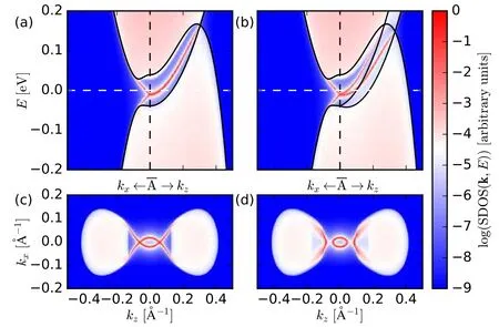
Fig.11. Surface states on the(010)-surface obtained from a k·p model for ZrTe with Eq.(4). (a)The surface density of states(the black lines show the bulk dispersion for ky =0)and(c)the surface Fermi surface with inversion symmetry(those without inversion symmetry are shown correspondingly in(c)and(d)). Figure reused from Ref.[21].
It is insightful to look at the evolution of Fermi arcs from Dirac semimetal to TPTM.In a k·p-model for ZrTe proposed in Ref.[21],one can easily tune between inversion symmetric and asymmetric band structures. In Fig. 11, we compare the surface states obtained from this model with and without inversion symmetry. In the presence of inversion and TR symmetries, the two TPs merge into a four-fold degenerate Dirac point. Across all energies in the gap, the two hole pockets aroundare connected by two Fermi arcs and the surface state on the-axis is two-fold degenerate. Breaking of inversion symmetry then splits the Dirac point into two TPs. Each TP contributes a single non-degenerate surface state. Since the two surface states are split along the kz-axis, the Fermi arcs are not required to connect the two hole pockets. Instead,one finds a topological-insulator-like Dirac cone around A which is still protected by TR and σhsymmetries.
4.5. Magnetotransport
The topologically non-trivial nature of Weyl semimetals reveals itself most spectacularly in the so-called chiral anomaly of the quantum field theory, realized in negative magnetoresistance measurements.[30,83-88]The chiral anomaly effect was originally proposed in high-energy particle physics,where it was referred as the Adler-Bell-Jackiw anomaly.[30,83-87]Weyl semimetals provide an excellent platform to study the chiral anomaly effect in condensed matter systems. In presence of a parallel magnetic (B) and electric field (E), the resistivity of Weyl semimetals decreases(i.e. conductivity increases) with increasing B-field in a finite range. This phenomenon is related to the chiral anomaly,and is generally referred as negative magnetoresistance. Although magnetoresistance is known to be positive in most of the known topologically trivial materials,negative magnetoresistance is quite rare. Negative magnetoresistance has been experimentally observed in several topologically non-trivial systems having non-zero Berry curvature near the Fermilevel.[89-94]Here,it is important to note that negative magnetoresistance could also appear in topologically trivial systems through giant magnetoresistance effect and/or current-jetting effect.[93,95]
In a Weyl semimetal, when an external B-field is applied parallel to an E-field that is orientated along a momentum direction connecting two opposite Weyl nodes, a chiral Weyl charge imbalance occurs. The applied B-field induces a charge pumping from one Weyl node to another Weyl node having opposite chirality separated in momentum space along the B ‖ E direction. This charge pumping process breaks the conservation of chiral charge,however,it retains the total charge conservation.The rate of charge pumping(W)between two opposite Weyl nodes can be described by equation[86,96]
Since the chiral charge pumping rate is proportional to E·B, negative magnetoresistance is expected to vary with the changing E and B field directions. However, if negative magnetoresistance is too sensitive to the relative orientation of E and B fields (i.e., it disappears after changing the relative angle between E and B field directions by 1°-2°),it might not be a signature of the chiral anomaly effect,rather it could originate from the classical current jetting effect.[93,95]The current jetting effect is a geometric effect which occurs when the current forms jets flowing along the high conduction directions in materials having large conductance anisotropy.[93]Therefore,it is important to carefully check the origin of negative magnetoresistance in topological materials.
Large negative magnetoresistance has been observed in Dirac/Weyl semimetals and in triple-point metals.[90,93,97-108]In Dirac semimetals or in triple-point metals, a Dirac point or a triple-point,respectively,splits into a pair of Weyl points in presence of a magnetic field, which gives rise to negative magnetoresistance under strong B field(‖E)at low temperatures. Type-I Weyl points produce a gapless Landau level spectrum in a magnetic field, whereas type-II Weyl points have an anisotropic chiral anomaly,[11]where the Landau level spectrum is gapless only for certain directions of the applied magnetic field. Therefore, the negative magnetoresistance is strongly anisotropic in type-II Dirac/Weyl semimetals, as observed in type-II Dirac semimetal PtSe2[96]and in type-II Weyl semimetal WTe2.[106,108-110]Therefore,the magnetotransport properties of TPs primarily depend on the direction of the applied magnetic field.AC3symmetry preserving magnetic field(along the C3-axis) does not gap the Landau level spectrum of a TP, but instead each TP contributes a single chiral Landau level (see Fig. 12). However, if the field is applied in a C3-breaking direction, the Landau level spectrum becomes gapped. Such a directional dependence also occurs in Dirac semimetals.[111]
The Landau levels are obtained by performing a Peierls substitution of kxand kyin the k·p Hamiltonian by kx=andthe magnetic length and a†, a the raising and lowering operators,In Fig. 12, we show the Landau level spectra of CuPt-ordered InAs0.5Sb0.5and ZrTe.[20,21]When the magnetic field is turned on,a pair of TPs turns into two crossing chiral Landau levels with opposite chirality. Due to the gapless Landau level spectrum, strong signatures of the TPTM state are observable in magnetotransport. Analogous to the chiral anomaly, one can create a Z2anomaly by applying parallel magnetic and electric fields.[112]
Magnetotransport experiments in the TPTM WC confirm the presence of direction dependent negative magnetoresistance for parallel magnetic and electric fields.[34]Due to the material growth constraints,the longitudinal magnetoresistance has been only measured in directions orthogonal to the(001)axis. Further investigations are required to confirm that the negative magnetoresistance stems from the TPs. We refer the reader to Refs.[93],[113],and[94]for a more comprehensive review on the transport property of topological semimetals.

Fig. 12. (a) Landau levels in CuPt-ordered InAs0.5Sb0.5 with a magnetic field of 50 T applied parallel to the C3 axis using the k·p-model of Eq. (9) and (b) those in ZrT with a magnetic field of 20 T applied parallel to the C3 axis using the k·p-model of Eq.(3). The dashed red lines show the bulk bands. Figure adapted from Refs.[20]and[21].
In addition to the negative magnetoresistance, the topological non-trivial features of electronic bandstructure and Fermi-surface are manifested in distinct quantum oscillations in the resistivity(ρ)data at strong B-field. Under the application of a strong B-field, the electronic bandstructure evolves into a set of 1D Landau levels, as shown in Fig. 12, and these Landau levels yield quantum oscillations (Shubnikovde Haas oscillations) in the ρ(B) data at low temperatures.These oscillations can be described using Lifshitz-Kosevich formula[114,115]ρ ~cos[2π(F/B+φ)], where F and φ represent the oscillation frequency and phase shift, respectively.Depending upon the topological nature and morphology of the Fermi-surface, φ could attain different values. For topologically trivial materials having parabolic band dispersion near the Fermi-level (i.e., zero Berry phase), φ = ±1/2 (in 2D)and ±5/8 (in 3D). Here +/- refers to hole/electron carriers. In case of Dirac/Weyl semimetals, the linearly dispersing bands near the Dirac/Weyl points inherit π Berry phase,which results inphase shifts of φ = 0 (in 2D) and ±1/8 (in 3D).[30,116-119]TPTMs are hybrid between Dirac and Weyl semimetals,hosting a topologically non-trivial nodal line near the Fermi-level, therefore an anisotropic phase shift which is sensitive to the orientation of the Fermi-surface cross-section and B-field is expected. An electron traversing along a closed path parallel to the nodal line plane,or along a perpendicular circle enclosing the nodal line, could acquire a Berry phase of 0, or π, respectively.[120]Hence, different phase shifts (φ= ±1/8 or ±5/8) could be observed depending upon the direction of the B-field and Fermi-surface cross-section. An excellent discussion related to the quantum oscillations and φ values for different topological semimetals can be found in Ref.[115].
5. Topology of phonons in triple-point metals
After describing the topological electronic properties of triple-point-metals, we shift our focus to the topological vibrational properties of these compounds. The concept of topology from the electronic bandstructure has been successfully extended to the vibrational bandstructure of materials.[121-125]In recent works, topologically protected band-crossings have been reported in the phonon spectrum of solid state crystals.[42,126-129]Soon after the theoretical prediction of double-Weyl phonons in the phonon spectrum of transition-metal monosilicides MSi (M = Fe, Co, Mn, Re,Ru),[126]Miao et al.[130]experimentally reported the first observation of double Weyl points in FeSi by means of inelastic x-ray scattering measurements. This paved the way for realization of novel phononic (bosonic) quasiparticle excitations and the associated topological properties in condensed matter systems. Several other studies focused on the topology of phonons in model systems, and predicted novel quantum phenomena arising due to the non-trivial topology of phonons, such as quantum Hall conductance, quantized phonon Berry phase, topologically protected pseudo spinpolarized interface states,phonon pseudospin Hall effect,valley effects of phonons,realization of phonon diode,and topological acoustics.[131-141]Recently, topologically protected Weyl nodal lines have been predicted in the phonon spectrum of bulk MgB2.[129]
Analogous to the physics of the electronic bandstructure, a nontrivial band-inversion between the low frequency acoustic and high frequency optical phonon modes results in topologically protected phonon band-crossings in the momentum space. Low frequency excitations of phonons near these topological band-crossing points could yield features of novel bosonic quasiparticles, such as Dirac, Weyl, and/or triple-point. Here, one main difference from the electronic structure stems from the fact that phononic excitations have bosonic character, whereas low-energy electronic excitations are fermionic. This rules out the applicability of the Pauli’s exclusion principle on phononic excitations in crystalline solids. In addition to the crystalline systems, topological bosonic quasiparticles have been realized in the photonic systems, metamaterials, and optical lattices.[142-151]Moreover,S¨usstrunk and Huber reported that oscillations of a simple pendulum in classic mechanical systems could also host topological bosonic modes.[123-125]
Although Dirac and Weyl phonon modes have been known since the last decade,[152]triple-point phonons joined the family of topological phonons only in 2018.[42,128]In Refs.[128]and[42],the existence of triple-point phonons was predicted in several special type-A triple-point metals having C3vsymmetry,such as ZrTe,HfTe,TiS,TaSb,and TaBi. Notably,these materials also host Weyl fermions and triple-point fermions in their electronic spectra. These binary compounds belong to space group #187 (P¯6m2) having 2 atoms in the primitive cell and thus,inheriting three acoustic and three optical branches in their phonon spectrum. When the mass difference(Δm=M-m,where M >m)between the constituent atoms is large,the direct frequency band gap between the optical and acoustic branches (Δg) is finite and positive at the A(0, 0, π/c) point of the hexagonal Brillouin zone. With decreasing Δm,the frequency band gap decreases systematically,and acoustic and optical phonon bands invert in the frequency space for certain binary compounds having small Δm. A necessary condition for such phonon band-inversion is[42]
Here, Δgis the direct frequency band gap at the A(0, 0, π/c)point of the Brillouin zone, β‖and β⊥are in-plane and outof-plane second-order interatomic force constants between the atoms of masses m and M,respectively.

Fig. 13. Phonon dispersion of (a) TaX (X = N, P, As, Sb) and (b) ZrY (Y = Se, Te) binaries calculated using the density functional perturbation theory (DFPT) for supercell of size 2×2×2. The mass difference Δm is provided in units of g/mol. A prototype crystal structure of TaSb is given in the inset. The primitive unit cell contains one Ta and one X (Sb)atom at(2/3,0.0,2/3)and(0.0,1/2,0.0)sites,respectively. TDP is marked in the phonon spectrum of TaSb and ZrSe along the Γ-A path. (c)An enlarged view of phonon dispersion in TaSb along Γ-A path. Colors and numbers depict distinct phonon modes. Arabic(Roman)numerals are used to mark phonon modes before(after)the band-inversion. Some data from Ref.[42]have been reused to produce this figure.
Figure 13(a)shows the calculated phonon spectra of TaX(X =N,P,As,Sb)binaries having Δm in decreasing order.[42]As the X atom in TaX gets heavier,the frequency of the optical phonon modes lowers, causing a systematic decrease in the frequency bandgap with decreasing Δm, and a phonon band-inversion takes place in TaSb along the Γ-A direction of the Brillouin zone, where two degenerate optical phonon modes acquire lower frequency than a non-degenerate acoustic phonon mode.This phonon band-inversion results in a gapless triply degenerate point(TDP)in the phonon spectrum of TaSb at frequency ~145 cm-1at q=(0,0,0.428). This point is marked in Fig.13(a). As shown in Fig.13(b), a similar mass induced phonon band-inversion also occurs in ZrY (Y =Se,Te)family. ZrY binaries are isostructural and isoelectronic to TaX.[128]In ZrTe, there exists a finite positive Δgdue to the relatively large Δm. Whereas,the net frequency gap closes in ZrSe,which has relatively smaller Δm,and Δgbecomes negative at the A-point due to the observed phonon band-inversion along the Γ-A path.
An enlarged view of the phonon dispersion along the ΓA direction of TaSb is shown in Fig.13(c). In this figure, the degeneracy of phonon modes and formation of a TDP can be clearly observed. Another TDP is located in other direction in the Brillouin zone at the same C3v-symmetric line. The two degenerate optical phonon modes participating in the phonon band-crossing at TDP correspond to the in-plane (x-y) optical vibrations of atoms, whereas the non-degenerate acoustic mode involved in the phonon band-crossing at TDP belongs to the out-of-plane(z)acoustic vibration of atoms. The competition between in-plane and out-of-plane interatomic force constants and Δm are the primary reason of the phonon-band inversion in TaSb and ZrSe.[42]
We note that the same methods[48,76]that are used to compute the topological character of electronic band-crossings can also be employed to evaluate the topology of phonon bandcrossings. However,it turns out that capturing the topology of phonon band-crossings is different from that of the electronic case. In case of non-interacting electronic systems, we analyze the symmetrized Hamiltonian of system for topological classification of the studied system, whereas, the topological classification of phononic systems can be built using the dynamical matrices D(q).
Similar to the case of triple-points in the electronic spectrum,[21]gapless TDPs in the phonon spectrum are connected by a gapless nodal line in the phonon frequency space.This nodal line,shown in Fig.14(d),is formed by the degenerate optical phonon modes near the TDP,and it is being protected by the C3vrotational symmetry of the crystal. Under the C3vsymmetry,the xx and yy interatomic force constants transform just like the pxand pyorbitals in C3vgroup,forming a 2D irreducible representation E,which enforces the degeneracy of the optical phonon modes along Γ-A. Computation of Berry phase (φB) using the Wilson loop approach along path S1, as shown in Fig.14(d),reveals φB=0 for the gapless nodal line connecting two TDPs.[42]
In order to reveal the topology of a TDP,one can split the two connected TDPs by breaking the C3vsymmetry. This can be done by changing the xx and yy entries in D(q), which is equivalent of tuning the interatomic force-constants(or equivalently,classical spring constants)between atoms along x and y directions.[42]This trick lifts up the degeneracy of the optical phonon modes,as shown in Figs.14(b)and 14(c),and enables us to probe the topological nature of TDP.It is worth noting that the aforementioned trick does not destroy the gapless nodal line, rather it results in a gapless nodal loop formed by the inverted optical and acoustic phonon bands(see Figs.14(e)and 14(f)). We can now define a path S2(and S3) enclosing the gapless nodal loop, and compute the φBusing the Wilson loop as demonstrated in Figs. 14(e) and 14(f). This calculation results in φB=π for S2and S3paths,thus confirming the topological nature of the TDP.[42]The mentioned technique is analogous to splitting two triple-point nodes in the electronic spectrum into four Weyl nodes by applying a Zeeman field.[21]

Fig.14. (a)The phonon spectrum of TaSb along the C3v-symmetric line of the Brillouin zone: doubly degenerate phonon bands(4,5)and(iv,v)can be seen. (b)The phonon spectrum of TaSb with the xx and yy force constants in the dynamical matrix made unequal for Ta. The degeneracy of(4,5)and(iv,v)is lifted. (c)The phonon spectrum of TaSb with the xx and yy force constants in the dynamical matrix made unequal for Sb. The degeneracy of(4,5)and(iv,v)is lifted. (d)The non-topological open nodal line formed in the BZ by bands iv and v of panel(a). The loop S1 encircles this line,but φB(S1)=0. (e)The closed nodal loop formed by bands iv and v in the BZ for the case of panel(b)away from the Γ-A line. The contour S2 links with this loop and φB(S2)=π. (f)The closed nodal loop formed by bands iv and v in the BZ for the case of panel(c). For a contour S3 linked with this loop,φB(S3)=π. Figure adopted from Ref.[42]with permission.
The nontrivial topology of phonon band-crossings in bulk indicates the presence of nontrivial surface phonon states.[42]In fact,Li et al. predicted unusual phonon surface states(open gapless arcs) in TiS and HfTe compounds, which are triplepoint metals hosting TDPs.[128]
6. Thermoelectricity in triple-point-metals
Since the nontrivial topology of electronic bands is often manifested in the electronic transport measurements, the phonon topology could have observable signatures in the lattice thermal transport measurements. It has been reported that topologically protected nontrivial phonon band-crossings introduce robust phonon-phonon scattering centers that enormously suppress the lattice thermal conductivity (κph) in triple-point metals hosting TDPs.[42]In Fig. 15(a), we compare the κphof two isostructural and isoelectronic triple-point metals TaN and TaSb,where the later hosts TDPs whereas the former does not. We notice that the overall κphin TaSb is almost three orders in magnitude smaller than that in TaN.Such a large reduction in κphcauses a direct benefit towards the improved thermoelectric performance of triple-point metals hosting TDPs.[42]
The thermoelectric figure of merit,ZT =S2σκel+κphT,is the key indicator of the thermoelectric performance of any material. To achieve large ZT, one requires large thermopower or Seebeck coefficient (S), high electrical conductivity (σ),low electronic thermal conductivity(κel),and low lattice thermal conductivity (κph) at a given temperature (T). Unfortunately, σ and κelare intrinsically coupled following the Wiedemann-Franz law, i.e., κel= L0Tσ, where L0is the Lorenz number.[153]Therefore,an optimal balance is required between σ and κel. Another key factor is the thermopower or Seebeck coefficient(S)which is primarily governed by the electronic electronic density of states near the Fermi-level.Generally, narrow bandgap semiconductors (with small κel+κph) exhibit the best thermoelectric performance (ZT ~2-3)when slightly doped by n- or p-type charge carriers.[153-158]Whereas,metals are known to be poor thermoelectrics due to their large σ and large κel(because of no energy bandgap).Moreover,κphis also considerably large in most of the metals,thus,overall ZT is quite low in metals ranging from 0.0001 to 0.001.[159-161]
The triple-point metals hosting TDPs seem to be special metals having considerably large and sizable ZT. The maximum estimated ZT in triple-point metals hosting TDPs ranges from ~0.15 (at room temperature) to ~0.4 (at 800 K).[42]Remarkably, in HfTe (which is a triple-point metal hosting TDPs), the maximum estimated ZT ranges from 0.35 (at 300 K)to 0.42(at 800 K)for electron doping(see Figs.15(b)and 15(c)). Evidently, the thermoelectric performance of triple-point metals hosting TDPs is 2-3 orders in magnitude larger than that of the trivial metals.[42]
Two key factors combine to enhance the net ZT in triplepoint metals. First, the presence of TDP, which gives rise to reduced κph. Second,the nontrivial electronic band-crossings near the Fermi-level,i.e.,the presence of gapless Weyl/triplepoints fermions,yield large σ (unfortunately,κelis also large)as well as enhanced thermopower S. Notably, σ lies in the same order of magnitude (σ/τ ~1020Ω-1·ms-1at lowdoping concentrations,τ being the electron-phonon relaxation time) for all the yet studied triple-point metals.[42]Gapless points near the Fermi-level give rise to sharp enhancement in the electronic density of states near the Fermi-level,which increases S according to the Mahan-Sofo theory.[162]Thus,triple-point metals with TDPs inherit high S,high σ,and low κph,which consequently yields relatively better thermoelectric performance in such metals. Figures 15(b)and 15(c)compare the thermopower(S)and thermoelectric performance(ZT)of selected triple-point metals with and without TDPs in their phonon spectra. For more technical details regarding the calculation of vibrational and thermoelectric properties, we recommend the reader to Ref.[42].
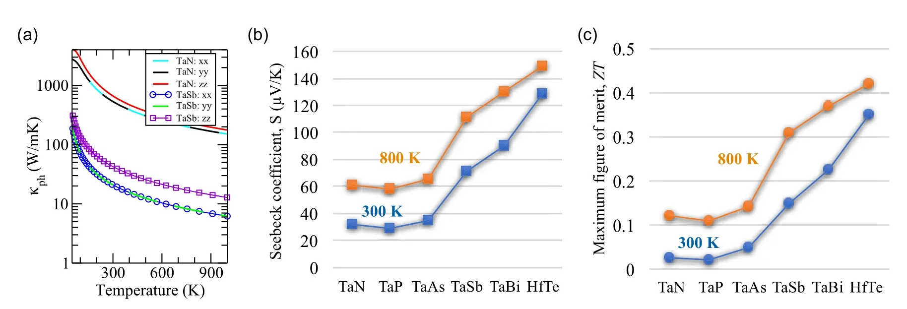
Fig.15. (a)Comparison of the calculated lattice thermal conductivity κph versus temperature data for TaN and TaSb binaries. Vertical axis is in logarithmic scale. (b) The maximum estimated thermopower or Seebeck coefficient, and (c) maximum estimated thermoelectric figure of merit computed at 300 K and 800 K for the electronic doping case. Data from Ref.[42]is reused to produce this figure.
7. Concluding remarks
We have overviewed the theoretical and experimental progress in the field of triple-point fermions protected by symmorphic symmetries. While the topological classification and basic band structure of triple-points are now well understood,open challenges lie ahead in investigating the transport and optical properties. In particular,low temperature applications could arise due to the presence of direction dependent magnetotransport.
Experimentalists are always in need of more accessible material candidates to confirm the manifold theoretical predictions. Recent experimental progress has been made for MoP,[36,37]where the existence of triple-points has been directly confirmed by ARPES, and WC,[34,35]of which the Fermi arcs and magnetotransport of triple-points have been investigated. To improve on this study, materials with good growth characteristics and well separated triple-points close to the Fermi level are desired. The recently predicted half-Heusler materials seem to have very favorable properties in this respect.[45]
Lastly,we have surveyed the topology of phonons in condensed matter systems,particularly in triple-point metals,and also discussed the numerical techniques required to evaluate the nontrivial topological nature of the triple-point nodes present in the phonon spectrum. The presence of topological phonon band-crossings usually introduces phonon-phonon scattering centers yielding low lattice thermal conductivity(phonon glass), whereas the presence of gapless topological nodes near the Fermi-level yields good electrical conductivity and thermopower (electron crystal). These two factors (electron crystal+phonon glass)combine to improve the thermoelectric performance of certain triple-point metals that host TDPs in their phonon spectra. Although the thermoelectric performance of triple-point metals is not comparable to that of the best known thermoelectrics(it is obviously expected given the metallicity), triple-point metals with topological phonon band-crossings rank much better when compared to ordinary metals in thermoelectricity.
To conclude,the discovery and description of triple-point metals will allow for further progress in understanding topological phenomena in solids and identification of topological materials with potential applications in technology.The triplepoint fermion has been accepted as an integral part of the family of topological(semi-)metals.
Acknowledgments
Special gratitude goes to QuanSheng Wu,who made significant contributions to the understanding and illustration of the triple-point metal physics. We would also like to thank Z.Zu,J.Li,P.Krogstrup,and M.Troyer,with whom we collaborated on the fermionic part of our research. We acknowledge A.H.Romero and C.Yue,who made significant contribution to our study of the phonon topology.We also thank D.Gresch,T.Hyart,R.Skolasinski,J.Cano,J.W.Liu,C.M.Marcus,and M.Wimmer for useful discussions.
- Chinese Physics B的其它文章
- Coercivity mechanisms in nanostructured permanent magnets∗
- Progress in recycling of Nd-Fe-B sintered magnet wastes∗
- Grain boundary restructuring and La/Ce/Y application in Nd-Fe-B magnets∗
- Local evolutions of nodal points in two-dimensional systems with chiral symmetry∗
- Structural,elastic,and electronic properties of topological semimetal WC-type MX family by first-principles calculation∗
- Scanning tunneling microscopic investigation on morphology of magnetic Weyl semimetal YbMnBi2∗