一种超低功耗的全CMOS基准电压源设计
2020-08-14 09:59:10王梓淇王永顺陈昊
现代电子技术
2020年16期
王梓淇 王永顺 陈昊
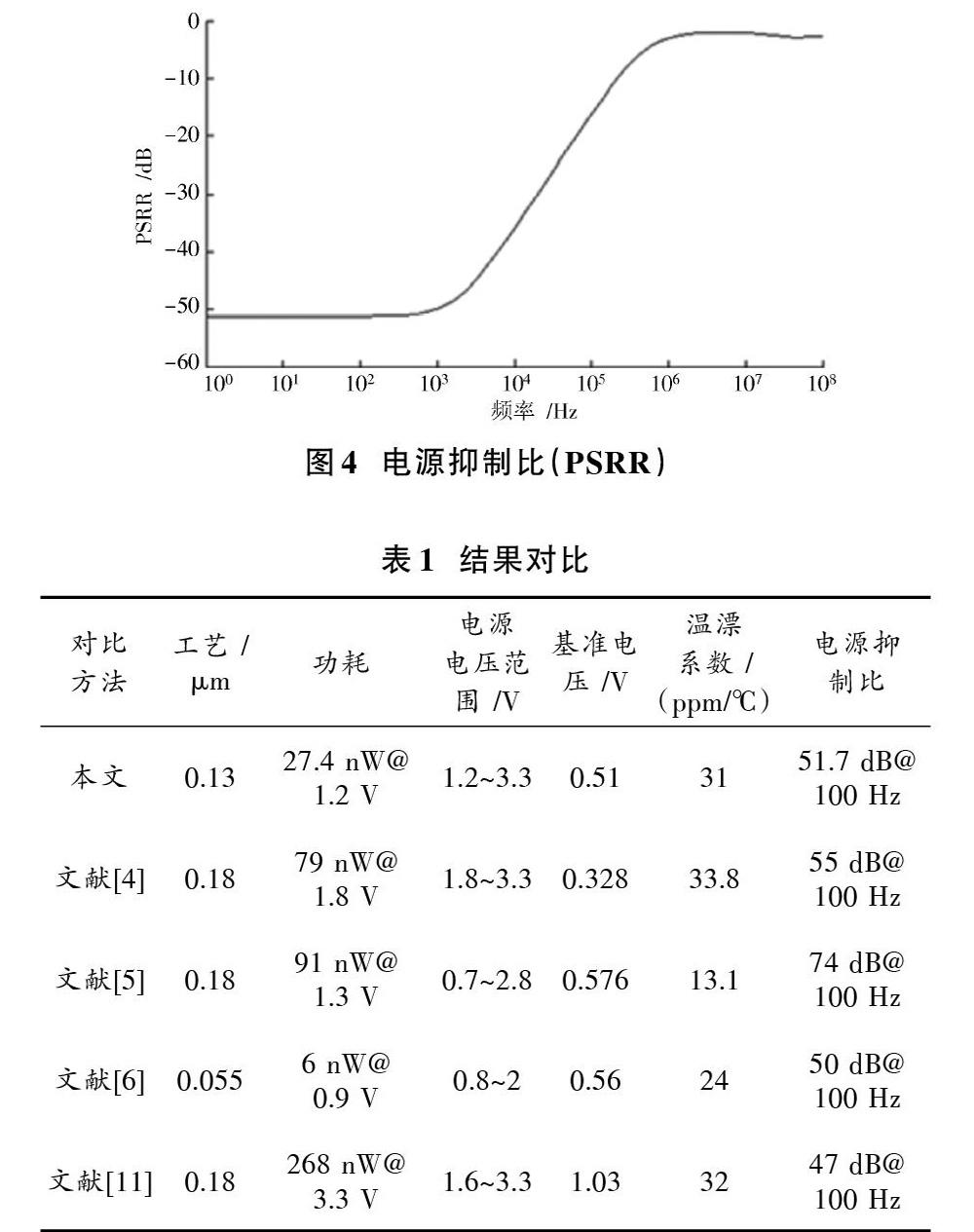
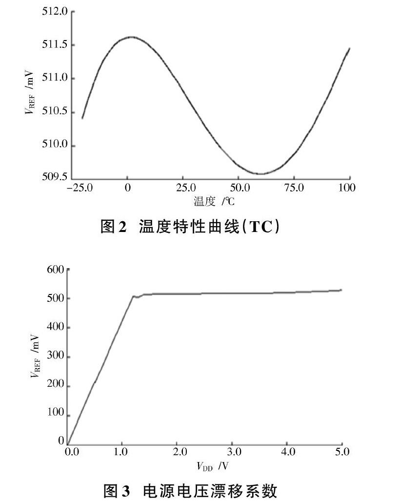

摘 要: 基于SMIC 0.13 μm CMOS工艺,设计一款纳瓦级功耗的全CMOS带隙基准电路。该电路由全CMOS电路实现,避免使用三极管和电阻,实现了节省芯片面积的目的。晶体管工作在三极管区和亚阈值区,大幅降低了功耗。Cadence仿真结果表明:在-20~100 ℃范围内,温度系数为31 ppm/℃;在电源电压1.2~3.3 V的变化范围内,电源电压漂移系数为0.42%/V。参考电源电压下,电路的电源抑制比(PSRR)达到51.7 dB@100 Hz;室温下,电路总静态电流为22.8 nA,功耗为27.4 nW@1.2 V;该电路可调节性强,适用于低功耗芯片中。
关键词: 全CMOS; 带隙基准; 基准电压源; 电路设计; 超低能耗; Cadence仿真
Abstract: A nava?level power?consumption full?CMOS band?gap reference circuit is designed based on SMIC 0.13 μm CMOS technology. The circuit is realized by full?CMOS circuit, and the use of BJTs and resistances has been avoided, and the chip area has been saved. The transistor works in the triode region subthreshold region, which greatly reduces the power consumption. The Cadence simulation results show that the temperature coefficient is 31 ppm /℃ when the temperature ranges from -20 ℃ to 100 ℃. The drift coefficient of power supply voltage is 0.42%/V within its range from 1.2 V to 3.3 V. The circuit′s PSRR can reach 51.7 dB@ 100 Hz under the reference voltage. At room temperature, the total quiescent current of the circuit is 22.8 nA, and the power consumption is 27.4 nW@1.2 V. This circuit has strong adjustability and is suitable for the low?power consumption chip.
Keywords: full CMOS; band?gap reference; reference voltage source; circuit design; ultra?low power consumption; Cadence simulation
带隙基准电路是每个模拟电路的核心组成部分之一。带隙基准的输出电压要求不随电源电压的变化而变化,为后续模块提供稳定的输入电压和电流。可穿戴集成电路应用非常广泛,小到智能手表,大到人体肢体助力机器人应用的兴起。集成电路设计对带隙基准电路提出了更低的功耗、更高的稳定性等要求[1]。
带隙基准的应用非常广泛,如在AD/DA,DC?DC,LDO等集成芯片中,在设计上可大致分为两大类:全CMOS带隙基准和非全CMOS带隙基准。本文提出一款全CMOS带隙基准,不包含三极管(BJTs)和电阻(Resistances)。 随着工艺的进步,工艺尺寸越来越小,晶体管启动所需要的阈值电压([VTH])也随之降低,但是亚阈值电压变化范围较大,给设计带来了一定的难度。
如今很多晶体管和电路结构不再需要1.2 V的基准电压,在这样的趋势下,全CMOS带隙基准电压源得到迅速发展。这种结构大幅减小了芯片面积,节约成本。本设计基于SMIC 0.13 μm工艺,实现了良好的温漂系数及超低功耗。……
登录APP查看全文