
In-situ fabrication of ZnO nanoparticles sensors based on gas-sensing electrode for ppb-level H2S detection at room temperature∗
2021-03-11 08:32JingYueXuan宣景悦GuoDongZhao赵国栋XiaoBoShi史小波WeiGeng耿伟HengZhengLi李恒征MeiLingSun孙美玲FuChaoJia贾福超ShuGangTan谭树刚GuangChaoYin尹广超andBoLiu刘波
Chinese Physics B 2021年2期
Jing-Yue Xuan(宣景悦), Guo-Dong Zhao(赵国栋), Xiao-Bo Shi(史小波), Wei Geng(耿伟),Heng-Zheng Li(李恒征), Mei-Ling Sun(孙美玲), Fu-Chao Jia(贾福超),Shu-Gang Tan(谭树刚), Guang-Chao Yin(尹广超),‡, and Bo Liu(刘波),§
1Laboratory of Functional Molecular and Materials,School of Physics and Optoelectronic Engineering,Shandong University of Technology,Zibo 255000,China
2Institute of Artificial Intelligence,Henan Finance University,Zhengzhou 450046,China
Keywords: ZnO,H2S gas sensor,room temperature
1. Introduction
ZnO,as one of the important n-type metal oxide semiconductors, has attracted wide attention in gas-sensing applications due to its advantages of low-cost,non-toxicity,and high mobility of conduction electrons.[1–8]Recently, many ZnObased nanomaterials have been used to detect H2S and have exhibited a good response and selectivity, so it has been regarded as one of the most promising H2S sensing materials.However, in most work, the ZnO sensors generally require a high operating temperature(around 200–450◦C),[9–16]which inevitably increases the energy consumption,shortens the life of the device, thereby extremely limits the practical application. Thus, achieving room-temperature detection of lowconcentration H2S is of significant importance.
In order to achieve room-temperature detection of H2S, many works concentrate on compounding with noble materials[17]or other semiconductor materials, doping by other elementals,[18–20]or testing under assistance of UV-illumination,[21,22]which obviously require complex processes, expensive equipments, and high production costs. So far,unmodified ZnO nanomaterials used as room-temperature H2S sensors have rarely been reported yet. According to the typical gas-sensing mechanism,that is,the gas sensing behavior is related to the redox reaction of surface electrons and target gas,which extremely depends on the specific surface area of the sensors. Therefore,decreasing the grain size of the sensors for larger specific surface areas via morphology regulation may be a promising strategy. For example,Patil et al.[23]prepared ZnO nanoparticles with sizes of 18–40 nm by successive ion layer adsorption and reaction(SILAR)technique to detect NO2at low temperature(150◦C).Deng et al.[24]synthesized ZnO quantum dots with average grain size of 14.6 nm via a colloidal procedure to detect H2S at 90◦C. In addition, the device structure of the gas sensor also plays a vital role in improving the effective specific surface area of the sensors. For a typical gas-sensing device,the gas-sensing materials generally are coated on the prefabricated ceramics plate’s electrodes by a screen-printing or doctor-blading method, then annealed at an appropriate temperature to form a film for the gas-sensing detection.[25,26]However,it will inevitably cause the problem of large thickness and material agglomeration,as a result,only a small portion of gas-sensing materials can be exposed to the gas atmosphere for reacting with the target gas.[27]Based on the above considerations,synthesizing small-sized nanomaterials and controlling the thickness of the material may be a promising strategy.
In this work, a simple sol-gel method is used to synthesize nano-sized ZnO nanoparticles (NPs), a facile dropcoating technology is used for in-situ preparation of ZnO NPs on the gas-sensing electrode with controllable thickness. Asprepared ZnO NPs sensors will measure low-concentration H2S at room temperature to study their response/recovery speed, response value, minimum detection limit, and selectivity nature. In addition, the effect of the calcine time and thickness of the film on gas-sensing performance will be investigated,and the corresponding physical mechanism of H2S detection will also be discussed.
2. Experiments and methods
The preparation and measurement processes of gas sensors are shown in Fig.1,which is further explained in detail in the following part.
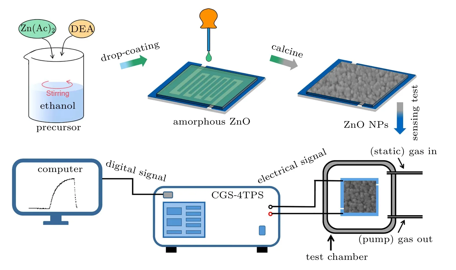
Fig.1. Preparation schematic of ZnO NPs on the gas-sensing electrode,and sketch of the intelligent gas-sensing test system.
2.1. Synthesis of ZnO NPs sensors
The alumina-based plate-type electrode was used as a gas-sensing electrode, which has five pairs of Ag–Pd fingers with 200µm in separation as the electrode materials. Before the preparation of ZnO sensors,the gas-sensing electrode was cleaned ultrasonically with acetone,isopropanol,ethanol,and deionized water for 30 min in turn respectively, and subsequently dried with nitrogen.
The ZnO NPs sensors were in-situ fabricated on the electrode by a simple sol-gel method and drop-coating technology.Firstly, 40 ml of an aqueous solution containing 0.05 M zinc acetate and 0.05 M diethanolamine was prepared at 30◦C in advance.Then,the gas-sensing electrode was placed on a level surface(calibrated by bubble level). Next,a capillary(diameter of about 1 mm)was used to take a drop of the seed solution(about 0.02 g) to the center of the electrode. Finally, the solution was free to diffuse and allowed for air dry (40 s). The above steps are defined as one cycle. At this time,the relative humidity is 50% and the operation temperature is room temperature. Finally, the gas-sensing electrode was calcined for a certain time at 400◦C to obtain ZnO NPs films. To study the effect of the calcining time, the number of cycles was set to 2, and the calcining time was set to 30 min, 60 min, and 120 min,hereinafter designated as T-30,T-60, and T-120,respectively. To study the effect of the thickness of the films,the calcining time was set to 30 min firstly, the number of cycles was set to 2, 4, and 6, which were denoted as C-2, C-4, and C-6,respectively.
2.2. Characterizations and gas measurement
The morphologies and microstructure of the ZnO NPs sensors were examined by a scanning electron microscope(SEM,SU8010)and high-resolution transmission electron microscopy(HRTEM,JEOL JEM-2200FS),respectively. The xray diffraction(XRD,Germany BrukerAXS D8 Advance)pattern was used to confirm the crystalline structure of the samples. The gas-sensing properties were tested using an intelligent gas-sensing analysis system (CGS-4TPS, Ltd, China).The response value of gas sensors is defined as the ratio of the resistance of the ZnO NPs sensor exposed to air(Ra)and target gas(Rg)atmosphere,which can be expressed as

3. Results and discussion
3.1. Morphology and structure
The morphologies, microstructures, and elemental composition distributions of the ZnO NPs films prepared with different conditions are investigated in Fig.2. As shown in Figs. 2(a) and 2(b), the circuit of the gas-sensing electrode consists of five pairs of interdigital fingers,where the distance between the interdigital fingers is about 200µm.In Figs.2(c)–2(e),the morphologies of T-30,T-60,and T-120 are shown. It can be seen that all samples show relatively regular spherical particles. As the calcining time increases, the grain size(diameter) of the ZnO NPs gradually increases. The average grain sizes of T-30,T-60,and T-120 are about 16 nm,21 nm,and 28 nm, respectively. In addition, as the calcining time increases, the uniformity of the ZnO NPs is weakened. In particular, a small number of large particles appear in T-120,which may form by agglomeration of small particles. Figure 2(f) shows the HRTEM images. Several fringe patterns can be obviously seen,where the lattice spacings of 0.247 nm,0.26 nm,and 0.281 nm can correspond to the interplanar distances of the {101}, {002}, and {100} facets of hexagonal ZnO(JCPDS No.36-1451). The EDX elemental mapping images of the ZnO NPs sensor are shown in Fig.2(g). Among them,Al and Ag elements should derive from the gas-sensing electrode. The sufficient Zn and O elements can further indicate that ZnO NPs have been successfully prepared.

Fig.2. SEM images of(a),(b)bare gas-sensing electrode,(c)T-30,(d)T-60, and (e) T-120. (f) HRTEM image of T-30. (g) EDX elemental mapping images of ZnO NPs sensor.
Figure 3 shows the XRD patterns of the samples with different condition to further confirm the crystalline structure and study the effect of the calcine time on ZnO.In order to avoid the interference caused by the high diffraction signal of alumina substrate and Ag circuit, an ordinary amorphous glass without obvious diffraction peak(black line) was used as the preparation substrate of ZnO NPs. When ZnO NPs were synthesized on the glass substrate, several obvious characteristic peaks appear at 31.8◦, 34.4◦, 36.3◦, 47.5◦, 56.6◦, and 62.9◦,which correspond to (100), (002), (101), (102), (110), and(103)facets of hexagonal ZnO(JCPDS No. 36-1451),respectively. As the calcine time increases,the position and number of characteristic diffraction peaks have no change. However,the intensity and sharpness of the diffraction peaks significantly reduce,especially for the sample with 120 min calcine time. This may be due to the fact that the increase of the grain size of ZnO NPs causes the spread of full width half maximum(FWHM)of the diffraction peaks,which corresponds to the SEM results.

Fig.3. The XRD patterns of substrate and ZnO NPs sensors with different calcine time.
3.2. Gas sensing properties and mechanism
The H2S sensing characteristics of the ZnO NPs sensors with different conditions were measured at room temperature.As shown in Fig.4(a), the gas-sensing performance of ZnO NPs obtained with different calcine time for 750 ppb H2S is compared.It can be seen that as the calcination time increases,the response value decreases. The response values of T-30,T-60, and T-120 are 73.3%, 35.2%, and 6.9%, respectively.The decrease of the response value should be related to the decrease in the specific surface area caused by the larger grain size. In addition, according to Ahn et al.,[28]the gas-sensing performance has a positive correlation with the oxygen defect density. Generally, a calcine process can reduce the defect density and increase the crystallinity of nanomaterials,which may further reduce the response values of T-60 and T-120.Except for the change of the response value, the response time and recovery time of T-60 (110 s, 106 s) and T-120 (120 s,118 s) are longer than those of T-30 (93 s, 90 s). This is because they are more difficult to reach the stable state compared to T-30 exposed to H2S at the same time, which may be due to the fact that the agglomeration of ZnO NPs hinders gas diffusion. Figures 4(c)and 4(e)show the gas-sensing characteristics of T-30, T-60, and T-120 exposed to different concentration H2S at room temperature. It can be seen that T-30 has the highest response value for all concentrations. And the response values of all samples show a well linear relationship with the H2S concentration,which will be beneficial for being quantified in the practical application. In Figs.4(b),4(d),and 4(f),the effect of the thickness of the ZnO NPs films on their H2S sensing performance is investigated. Obviously, there is a negative correlation between the response value and the film thickness in different concentration H2S.And compared with C-2,the response time and recovery time of C-4(95 s,120 s)and C-6(100 s,123 s)with larger thickness also increase. We compare our results with the previously reported ones(shown in Table 1),the ZnO NPs sensor exhibits much higher gas sensitivity and lower operating temperatures. The reason will be explained in the reaction mechanism below.
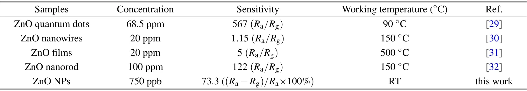
Table 1. H2S sensing properties of the different samples in our study and in the literature.

Fig.4. The gas-sensing characteristics of ZnO NPs sensors with(a),(c),(e)different calcine time and(b),(d),(f)different thickness exposed to different concentration H2S at room temperature.
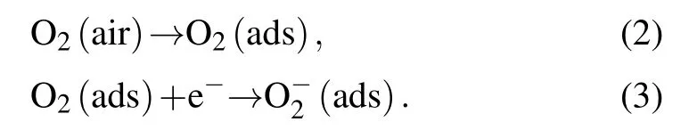
The reaction mechanisms between ZnO NPs and H2S will be explained by electron depletion layer and grain boundaries potential barrier theories.[33,34]As shown in the right panel of Fig.5, when ZnO NPs sensors are exposed to air, due to the fact that ZnO possesses an electron spin resonance signal reflecting the concentration of free electrons,and the freely conducting electrons on ZnO can interact equally with both oxygen nuclei,thus oxygen ions are adsorbed with the molecular axis parallel to the surface on ZnO.[35,36]At the same time,since the suspension bonds on the surface of nanomaterials introduce impurity energy levels in the semiconductor band gap,which can excite electrons and holes at lower temperatures,thereby enhancing the adsorption of oxygen and hydrated hydroxyl groups.[37,38]The oxygen adsorbed on the surface of ZnO will trap electrons in the conduction band of ZnO to form chemically adsorbed oxygen(O−2),thereby resulting in the formation of a wide electron depletion layer and the band bending upwards. Meanwhile,the high potential barrier appears in the interface of multiple ZnO NPs. Therefore, this process will make the resistance of ZnO NPs increase gradually and reach the maximum in dynamic balance. The above process can be described by[39–41]
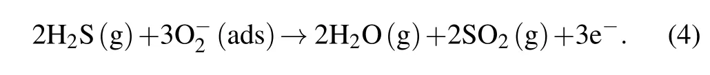
When ZnO NPs sensors are transferred to the H2S condition,the chemisorbed O2−reacts with H2S and returns electrons to the ZnO NPs. Thereby, the electron density near the surface of the ZnO NPs is increased (resistance is reduced), and the depletion layer is narrowed. Meanwhile,at the interfaces,the height of the grain boundary potential barrier is significantly reduced, which will reduce the obstruction to the transmission of electrons. In addition, the hydrated hydroxyl groups adsorbed on the surface of ZnO can saturate the suspension bonds on the surface of the ZnO NPs and reduce the electronic transition barrier, which will further reduce the resistance of the ZnO NPs sensors.[37,42]This process can be described by[9,10,17,43,44]
According to the above mechanism,the proportion of the depletion layer in the whole nanoparticle directly affects the gas-sensing response value. However,the thickness of the depletion layer cannot exceed the Debye length of nanomaterials. Thus, the larger grain size caused by longer calcine time will decrease the proportion of the depletion layer,and thereby decrease the response value. For the effect of the thickness of the ZnO NPs sensor, due to the accumulation of particles derived from gravity, except that a small part of the surface is porous, most of the surface is dense at the bottom (as shown in Fig.5(b)),which makes the effective thickness that participates in the response of ZnO NPs limited.For a similar reason,the increased thickness obviously decreases the proportion of the effective thickness in the whole film, finally resulting in the reduced response value of the ZnO NPs.

Fig.5. Schematic diagram and cross-section SEM of(a)C-2 and(b)C-6,as well as their schematic diagram of reaction mechanism in the right.
The selectivity nature of ZnO NPs sensors was also investigated. As shown in Fig.6(a), it can be seen that ZnO exhibits superior response value to H2S even at low concentrations. The response values of above several interference gases(such as formaldehyde, isopropanol, acetone, ethanol, acetic acid,methanol,H2,and NH3)with high concentration are also obviously lower than that of H2S.The excellent selectivity to H2S may be ascribed to the extra chemical reaction between ZnO and H2S, that is, H2S directly reacts with ZnO NPs to form ZnS. According to the previous researches, the formation of ZnS will introduce a shallow donor level in the band gap of ZnO NPs. When ZnO NPs sensors are thermally excited(above absolute zero),electrons transit from the shallow donor level to the conduction band of ZnO, further reducing the resistance and increasing the sensitivity. The corresponding reaction can be described by[45,46]

To prove the above reaction and study the degree of reaction,the H2S sensing tests were carried out in normal air and hypoxia environment, respectively, as shown in Fig.6(b). The hypoxia environment is realized through advance vacuum and 30 min N2flushing to exhaust O2. It can be seen that the response value to H2S is significantly reduced from 73.3% to 8%in hypoxia environment, which indicates the existence of the above reaction. Meanwhile, the rationality of the above mechanism can be confirmed, that is, H2S sensing behavior mainly relates to its reaction with chemisorbed O−2. However,the response and recovery processes are also different in the air and hypoxia environment. There is a complete response and recovery in air,while the response value of ZnO NPs cannot normally recover. This should due to the below reaction reported by Wang et al.:[46]

ZnS will restore to ZnO again with the assistance of O2. Thus,the reaction between ZnO with H2S is not a simple adsorption/desorption reaction. And this reaction can ensure repeatability and improve the selectivity of the H2S sensing behavior in an oxygen-containing environment.

Fig.6. (a)The selectivity nature of ZnO NPs sensors;(b)H2S sensing behaviors in air and hypoxia environment.
4. Conclusion
In summary, we fabricated ZnO NPs sensors based on gas-sensing electrode by a simple sol-gel method with shorttime calcine process to detect H2S.Under the synergistic effect of morphology control and device design,the as-prepared ZnO NPs sensors achieved the room-temperature detection of ppblevel H2S, the minimum detection limit reached 30 ppb and the response value was 7.5%. In addition,the effect of calcine time and thickness of film on H2S sensing behavior were investigated. The results indicate that shorter calcining time and thinner film thickness are beneficial to obtain a small particle size and increasing the effective surface area of the film, and thereby increase the H2S sensing performance of the ZnO NPs sensors.
猜你喜欢
音乐天地(音乐创作版)(2021年6期)2021-09-03
赤水源(2018年6期)2018-12-06
商周刊(2017年16期)2017-10-10
江苏教育(2017年45期)2017-07-05
金色年华(2017年10期)2017-06-21
初中生世界(2017年20期)2017-06-01
作文周刊·小学一年级版(2016年35期)2017-03-03
今古传奇·故事版(2016年22期)2016-12-24
中学生数理化·七年级数学人教版(2016年4期)2016-11-19
快乐作文·低年级(2015年3期)2015-03-26

- Chinese Physics B的其它文章
- Novel traveling wave solutions and stability analysis of perturbed Kaup–Newell Schr¨odinger dynamical model and its applications∗
- A local refinement purely meshless scheme for time fractional nonlinear Schr¨odinger equation in irregular geometry region∗
- Coherent-driving-assisted quantum speedup in Markovian channels∗
- Quantifying entanglement in terms of an operational way∗
- Tunable ponderomotive squeezing in an optomechanical system with two coupled resonators∗
- State transfer on two-fold Cayley trees via quantum walks∗