
Effect of hydrogen content on dielectric strength of the silicon nitride film deposited by ICP-CVD∗
2021-05-06 08:56YudongZhang张玉栋JialeTang唐家乐YongjieHu胡永杰JieYuan袁杰LuluGuan管路路XingyuLi李星雨HushanCui崔虎山GuanghuiDing丁光辉XinyingShi石新颖KaidongXu许开东andShiweiZhuang庄仕伟
Chinese Physics B 2021年4期
Yudong Zhang(张玉栋), Jiale Tang(唐家乐), Yongjie Hu(胡永杰), Jie Yuan(袁杰),Lulu Guan(管路路), Xingyu Li(李星雨), Hushan Cui(崔虎山), Guanghui Ding(丁光辉),Xinying Shi(石新颖), Kaidong Xu(许开东), and Shiwei Zhuang(庄仕伟),†
1School of Physics and Electronic Engineering,Jiangsu Normal University,Xuzhou 221116,China
2Jiangsu Leuven Instruments Co. Ltd,Xuzhou 221300,China
Keywords: dielectric strength, silicon nitride film, inductively coupled plasma chemical vapor deposition(ICP-CVD),hydrogen content
1. Introduction
Silicon nitride thin films are widely used in large-scale integrated circuits and semiconductor devices,[1]such as optoelectronics,microelectronics,and so on,[2]because of their excellent photoelectric performance,mechanical and passivation properties.[3]Demands for high-k films are becoming more and more urgent with the popularization of IC manufacturing process.[4]Silicon nitride films fabricated by inductively coupled plasma chemical vapor deposition (ICP-CVD) have found many applications in this field as passivation layers.[5]The low temperature of the deposition, the higher deposition rate,the adjustable refractive index,and the higher passivation quality are all reasons that silicon nitride films are increasingly supplanting other dielectric layers, such as SiO2.[6]In summary, silicon nitride layers are likely to lower the production costs and increase the efficiency of microcircuit.[7]
Due to the continuous shrinking of integrated circuits in the field of microelectronics,[8]the tunneling current is too large and the gate control force is reduced.[9]The traditional silicon dioxide dielectric layer no longer meets the needs of microelectronic devices,[9]so high breakdown voltage materials to replace the gate dielectric layer with low breakdown voltage have become another research hotspot in the world.[10,11]Regarding the preparation of high breakdown voltage films, the high breakdown voltage materials have many requirements,[5,12]for example, the dielectric constant must be as large as possible,and the dielectric material must be thermodynamically stable on the silicon substrate.[6,8,13]The current research work on breakdown strength has been carried out on PECVD/LPCVD,[10,14]but this experiment uses ICPCVD model to prepare silicon nitride film,which can provide more energy,promote the decomposition of reaction gas,and make a film with greater breakdown strength.
The hydrogen content in the silicon nitride film greatly affects the breakdown strength of the film.[15]Among the components of the film, the Si–H bond plays a fundamental role in the composition of the film. As the hydrogen content in the film changes, the electrical properties of the film will change.[6,16,17]When the hydrogen content in the film is high,the dangling bonds of silicon will be filled with H,which will increase the stability of the film and increase the breakdown strength.[18]However, regarding the relationship between the H content and film breakdown voltage,few experiments have been carried out on ICP-CVD machines, and the conclusions are not perfect,so our experiment uses ICP-CVD machines for film deposition.[19,20]
In this article, we changed the gas flow ratio and RF power to deposit silicon nitride films with different hydrogen contents. First, the deposition rate of the silicon nitride film was measured to reflect the growth state of the film. Then,the composition of the film was obtained by Fourier transform infrared spectroscopy(FTIR)and Raman spectroscopy. Combining the dielectric strength of the film, we can obtain the relationship between the hydrogen content of the film and the dielectric strength, which is of great significance for the control of the dielectric strength of the silicon nitride film.
2. Experimental procedure
2.1. Sample preparations
For all experiments, double-side polished, p-type (boron doped, > 50 Ω·cm) (100)-oriented single-crystalline 4-inch silicon wafers have been used as substrates,with a thickness of 350±15µm.[21]Before the film is deposited,the substrate is wiped with alcohol to remove the dirt on the surface to ensure the accuracy of the experiment.
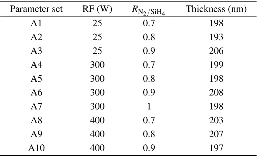
Table 1. Run list and results.
The deposition experiments were performed using a Leuven Instruments 3111 System ICP-CVD downstream reactor,with an additional capacitively coupled RF plasma source connected to the substrate electrode. Both plasma sources operate at a frequency of 13.56 MHz, whereas only the ICP source was activated during the deposition. The process chamber was evacuated to a base pressure of 15 mTorr, before N2and Ar were introduced together with SiH4via a gas distribution ring arranged next to the substrate electrode. The experimental plan is shown in Table 1. By adjusting the process conditions,it is ensured that the film thickness of the experimental samples is basically the same(about 200 nm), and the difference in film thickness is controlled so that the thickness will not become a factor affecting the breakdown voltage. The RF power was controlled at 25 W, 300 W, 400 W. On the other hand, under the same RF conditions, we controlled the ratio of N2/SiH4at 0.7,0.8,0.9,and 1.0,so that silicon nitride with different hydrogen content can be obtained. All depositions were performed at a substrate temperature of 150◦C. In order to reduce the deviation of the results,the first few samples of the machine were not recorded,and the experimental samples were made when the equipment was stable. And when the process conditions change,repeat the experiment first,and then make the samples when the machine adapts to the experimental conditions.
2.2. Analysis methods
The thickness d and refractive index n(at λ =632.8 nm)of the deposited thin films were determined using the spectral reflectance method. The measurements were conducted with a SpecEI-2000 spectroscopic ellipsometer, which determines the reflectance between 400 nm and 1000 nm. FTIR measurements on a SHIMADZU IRAffinity-1 infrared spectroscope in transmission mode between 350 cm−1and 7800 cm−1with a resolution of 0.5 cm−1were carried out to investigate the chemical composition of the films. The infrared spectrum of a blank silicon wafer was taken as reference. After baseline correction of the measured spectra, the absorption peaks were normalized by the film thickness and by the height of the silicon lattice absorption peak at 610 cm−1, assuming an equal thickness of the substrates. Room temperature Raman spectra were obtained by a Raman spectrometer(Horiba,LABRAM HR EVO)using a wavelength of λ =633 nm laser to investigate the micro-structural composition of SiNxfilms.The hydrogen content was measured by D-SIMS equipment(CAMECA 7f-auto)at about 200 nm in the SiNxfilms.
The dielectric strength was measured by applying a ramped voltage across the dielectric film. The film was deposited on a conductive bottom layer together with a metal layer deposited on top of the deposited film. The metal layer was patterned either through a shadow mask or by lift-off to form small test pads(0.05×0.05 mm). The voltage was then ramped up until a high current peak was observed, which is the breakdown of the film.[22]
3. Results and discussion
3.1. Deposition rate
First, ICP power has a very important influence on the film deposition rate.[23]As can be seen from Fig.1,when the ICP power is 25 W,300 W,400 W,the deposition rate of the film will increase with the increase of the RF power.However,when the ICP power is 25 W and the N2/SiH4ratio is 0.7,0.8,0.9,the film deposition rate is 70.6 nm/min,72.8 nm/min,and 75.7 nm/min, respectively. The increase is not obvious, indicating that the energy transport conditions are not reached,and the reaction of film deposition is not sufficient. When the ICP power is 300 W and 400 W,the film deposition rate increases significantly with the N2/SiH4ratio, which indicates that the ICP power above 300 W can already meet the current reaction and can provide good film deposition energy.
Another factor that affects the deposition rate is the gas flow ratio. The gases participating in the reaction in our experiment are N2and SiH4. Argon mainly plays the role of bombarding the plasma,but does not participate in the reaction of the experiment. Therefore,the ratio of N2/SiH4has a very important effect on the reaction.[24]It is worth noting that when the N2/SiH4ratio is 0.7 and the ICP power is 25 W, 300 W,400 W, the film deposition rate is 70.6nm/min, 72.4 nm/min,and 75.4 nm/min, respectively, and the deposition rate does not change much. The material transportation conditions in thin film deposition are limited, and the reaction of thin film deposition is not sufficient. When the ratio of N2/SiH4is 0.8,0.9,the film deposition rate is very obvious with the increase of the ICP power,which can indicate that the ratio of N2/SiH4above 0.8 can meet the current reaction and can provide sufficient gas supply.
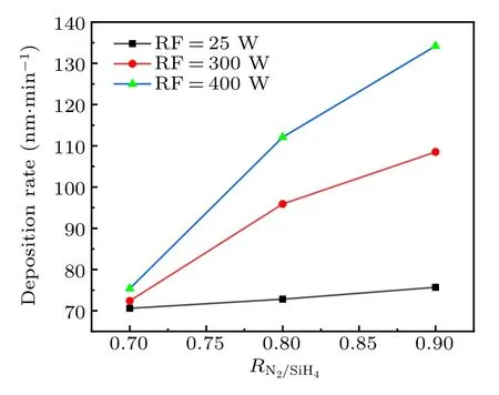
Fig.1. Variation of deposition rate under different RF power and N2/SiH4 ratio.
3.2. Chemical analyses
The conditions in Table 2 were used to deposit film samples A4, A5, A6, and A7. It can be seen from the FTIR diagram that when the flow ratio of N2/SiH4is changed, the chemical composition of the film also changes dramatically.In Fig.2, the absorption peak of the film is marked, from which the chemical bond density of the film and the chemical composition of the film can be known. First, the Si–H bond increases sharply with the increase of the N2/SiH4ratio. When the proportion of N2increases,the concentration of SiH4cannot keep up with the reaction concentration of N2,the decomposition rate of SiH4in the chamber will be suppressed,and the residual H will increase,which will make up for the Si dangling bonds of the SiH4during the reaction, thus the Si–H bond density will increase. The Si dangling bonds on the SiH4film are filled with H,which makes the film more stable,so that when electrons pass through the film, it is not easy to produce defects and be broken down,so the dielectric strength of the film is increased. Therefore, the dielectric strengths of A4,A5,A6,and A7 measured by the experiment increase sequentially, which is in line with theoretical expectations and can prove our conjecture. At the same time,the obvious peaks of the N–H bond and O-H bond of the A6 sample also indicate the increase in the H content in the sample, the increase in the probability of binding to N and O atoms,and the overall H bond density reaches the maximum. Finally, the Si–O and Si–N bonds of the A4, A5, A6, and A7 samples increase in turn, because the deposition speed of the film is accelerated,the formation of silicon nitride film increases,and the concentration of Si involved in the reaction also increases, making the film rich in silicon. This increases the refractive index and increases the overall stability of the film.
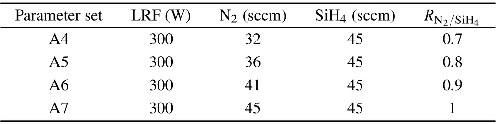
Table 2. Influence of the gas ratio on the infrared absorption peaks.
Fig.2. FTIR data of SiNx films.

Fig.3. Micro Raman spectra of A5,A6,A7. The inset shows the general scan.
Micro Raman spectroscopy(Fig.3)was used to confirm the phase of the deposited silicon nitride. The general scans for A5,A6,A7 samples are shown in the inset. Sharp peak at 520 cm−1is of Si (substrate used for deposition) with peaks around 950 cm−1confirming the presence of SiNx. It can be seen from the figure that the intensity of Si–N bonds of the A5,A6,and A7 samples increases sequentially,and it can be concluded that as the N2/SiH4flow ratio increases,the deposition concentration of silicon nitride increases. It is mutually confirmed with the conclusion drawn in FTIR that the intensity of Si–N bonds in the film increases, and the stability increases correspondingly, thereby increasing the dielectric strength of the film.
3.3. The hydrogen content in the films
In order to obtain the distribution of hydrogen in the film,D-SIMS equipment was used to measure the hydrogen content in the silicon nitride film (as shown in Fig.4). In the depth range of 0–100 nm, the hydrogen content of A5, A6, and A7 samples has little difference. Because in the shallow layer of the film, the gas flow has little effect on the deposition of the film,and a sufficient amount of gas can deposit silicon nitride films with almost the same composition and chemical bonds.At the depth of 100–120 nm, the hydrogen content of the A5 sample begins to drop sharply. At this depth,under the experimental conditions of the A5 sample,the nitrogen flow rate is not enough to completely supply the reaction,the N–H bonds and Si–H bonds in the film are reduced, and the overall hydrogen content is reduced. At the depth of 180–200 nm, the hydrogen content of the A6 and A7 samples begins to gradually decrease, and the hydrogen contents of the A6 and A7 samples are almost the same. This depth is close to the base of the film,so the hydrogen content in the film will decrease.Under the experimental conditions of the A6 and A7 samples,the supply of nitrogen is saturated. Even if the ratio of N2/SiH4is increased, the hydrogen content in the silicon nitride film cannot be greatly changed. In the end,the hydrogen contents of the two samples are almost the same.
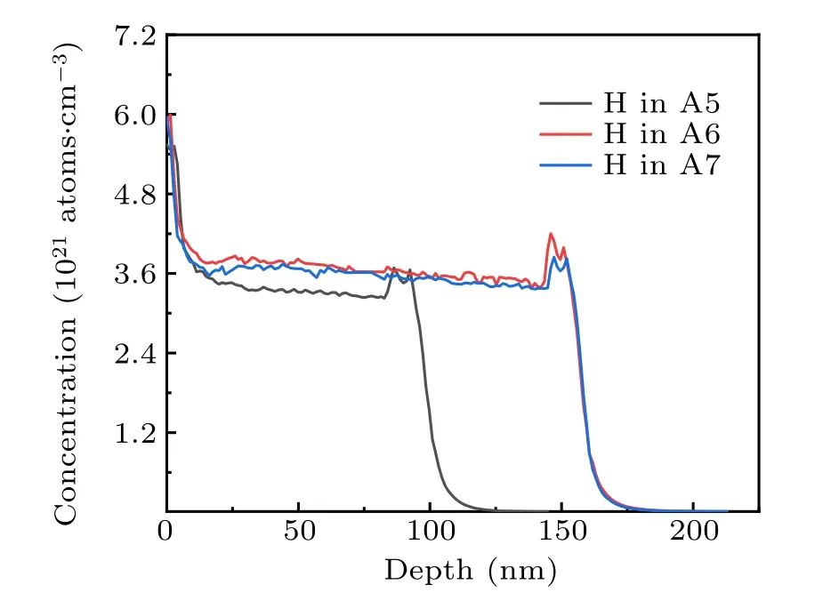
Fig.4. Hydrogen content in the films by D-SIMS.
3.4. Dielectric strength of the film
From Fig.5(a),we can explore the influence of N2/SiH4ratio and RF power on the dielectric strength. Based on the above discussion and the trend in the picture, we can clearly find that an increase in the proportion of N2/SiH4will lead to an increase in the dielectric strength. This is mainly because the increase in N2flow makes the dangling bonds of Si in the film replenished by H,which increases the ability of the film to store charges and thus increases the dielectric strength. On the other hand,increasing the RF power will reduce the dielectric strength of the film.When the power of the radio frequency increases,the number of holes in the film will increase,and the stability of the film will decrease, thereby reducing the ability to store charges, resulting in a decrease in the dielectric strength. When the RF power is 25 W,300 W,and 400 W,the dielectric strength of the film decreases sequentially,this is in line with our theoretical expectations.
The deposition rate of the film is also closely related to the dielectric strength.[25]From Fig.5(b), we can see that as the deposition rate increases,the dielectric strength of the film shows an upward and downward trend around 75 nm/min,and then shows a continuous upward trend after 80 nm/min. In the initial rising curve,when the deposition rate of the film increases,the material produced is mainly silicon nitride with a small amount of N–H and Si–H bonds, so the material tends to be stable and the dielectric strength of the film increases.With the further increase of the film deposition rate,the Si–H and N–H bonds in the film replace more silicon nitride,which leads to the instability of the material,so the dielectric strength of the film decreases. With the addition of a large number of Si–H bonds, the Si–H bonds in the film play a leading role,thereby increasing the role of H to compensate for the dangling bonds of Si,increasing the film’s ability to store charges and increasing the dielectric strength of the film.
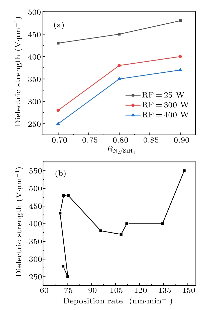
Fig.5. The effect of (a) and deposition rate (b) on dielectric strength.
4. Conclusion
In this work, the RF energy and gas flow are changed to obtain silicon nitride films with different hydrogen contents.The increase of the Si–N bond indicates that the silicon nitride content of the film is increased, and the film is more stable.Through the measurement of the dielectric strength of the sample,it is shown that lower RF power and higher N2/SiH4ratio will increase the dielectric strength of the silicon nitride film.Low RF power will increase the hydrogen content in the film,and hydrogen will not be combined with high energy to be discharged out of the chamber,so the dielectric strength will increase.A high ratio of N2/SiH4not only promotes the increase of N content in the film,but also increases the probability of Si bonding to form bonds,thereby forming more Si–H bonds in the film and increasing the hydrogen content in the film. It can be seen that increasing the hydrogen content in the film will increase the dielectric strength of the film, which is of great significance for the manufacture of films with high dielectric strength and has a wide range of MEMS applications.
猜你喜欢
家具与室内装饰(2022年5期)2022-06-22
家具与室内装饰(2022年3期)2022-04-20
家具与室内装饰(2022年2期)2022-04-19
Chinese Physics B(2022年1期)2022-01-23
选煤技术(2021年3期)2021-10-13
源流(2021年11期)2021-03-25
东坡赤壁诗词(2020年3期)2020-07-04
科学与财富(2019年31期)2019-10-21
世界家苑(2018年11期)2018-11-20
- Chinese Physics B的其它文章
- Speeding up generation of photon Fock state in a superconducting circuit via counterdiabatic driving∗
- Micro-scale photon source in a hybrid cQED system∗
- Quantum plasmon enhanced nonlinear wave mixing in graphene nanoflakes∗
- Restricted Boltzmann machine: Recent advances and mean-field theory*
- Nodal superconducting gap in LiFeP revealed by NMR:Contrast with LiFeAs*
- Origin of itinerant ferromagnetism in two-dimensional Fe3GeTe2∗