
A super-junction SOI-LDMOS with low resistance electron channel
2021-05-24 02:23WeiZhongChen陈伟中YuanXiHuang黄元熙YaoHuang黄垚YiHuang黄义andZhengShengHan韩郑生
Chinese Physics B 2021年5期
关键词:陈伟
Wei-Zhong Chen(陈伟中), Yuan-Xi Huang(黄元熙), Yao Huang(黄垚),Yi Huang(黄义), and Zheng-Sheng Han(韩郑生)
1College of Electronics Engineering,Chongqing University of Posts and Telecommunications,Chongqing 400065,China
2Institute of Microelectronics,Chinese Academy of Sciences,Beijing 100029,China
3University of Chinese Academy of Sciences,Beijing 100049,China
Keywords: LDMOS,breakdown voltage(BV),specific on resistance(Ron,sp),figure of merit(FOM)
1. Introduction
THE silicon-on-insulator lateral double-diffused metal–oxide–semiconductor (SOI-LDMOS) is widely adopted in power ICs due to its voltage control and high switching frequency characteristics.[1–3]For example, RF power LDMOS is widely used in wireless communication.[4]The breakdown voltage(BV)of reverse blocking and the specific on resistance(Ron,sp)of forward conduction are essential properties for the LDMOS,and the Baliga’s figure of merit(FOM)is proposed to evaluate the trade-off relationship between the BV and the Ron,sp. Many advanced structures are proposed to improve the FOM in recent years.[5–11]Specifically,the super-junction(SJ)technology is one of the most widely used methods. It can not only effectively reduce the Ron,spbut also increase the BV,and the FOM is significantly improved.[12–18]In the design of LDMOS, SJ is used in many structures. For example, the BSDSJLDMOS proposed by Duan Baoxing et al.[19]And,MFBLSJLDMOS proposed by Cao et al.[20]In addition,We realize the structure with lateral width variation using super-junction technology and call it VLW-LDMOS.[21,22]
In this paper,a SOI-LDMOS based on the super-junction technology with low resistance channel (LRC) is proposed.The charge compensation between the LRC and the superjunction are optimized to further improve the FOM.
2. Device structure and parameters
The structure of the proposed LRC-LDMOS is shown in Fig. 1. Compared with the conventional SJ SOI-LDMOS, a low resistance channel (LRC) is introduced on the surface of the drift region, which can significantly reduce the Ron,spof the device during the forward conduction state. At the same time, an SJ structure is designed directly below the LRC. In the reverse blocking state, it can not only completely deplete the LRC but also can optimize the surface and bulk electric field in the drift region.

Fig.1. Structure for the proposed LRC-LDMOS.
The key parameters of the conventional LDMOS(CONLDMOS),conventional SJ LDMOS(CON-SJLDMOS),variation of lateral width LDMOS (VLW-LDMOS), and the proposed LRC-LDMOS are designed to be the same. The thickness and length of the N-drift Tdare 5 µm and 16 µm, respectively. The doping concentration,thickness Tsubof p-type substrate are 8×1014cm−3and 2 µm, respectively. In addition, thickness Toxof buried oxide layer is 2 µm. For the CON-LDMOS,the doping concentration of the Ndriftis set as 2×1015cm−3. For the CON-SJLDMOS, the width and doping of the N-pillar and P-pillar are set to be the same with 0.5 µm and 1×1016cm−3. For the VLW-LDMOS, the doping concentration of the Nsjis set as 1.0×1016cm−3. For the LRC-LDMOS,the doping Nsjand thickness Tpof the N-pillar and P-pillar both are 5×1014cm−3and 4 µm, respectively.The length Lnof N-pillar and Lpof P-pillar are 0.7 µm and 1.3µm. The thickness Tcand doping concentration Ncof the LRC are 1 µm and 1×1016cm−3, respectively. The electrical characteristics of the device are designed and investigated with TCAD SENTAURUS. The physical and electrical models, including the mobility, ionization, and the recombination models are adopted in the simulation.
3. Electrical characteristics
3.1. The reverse breakdown voltage BV
Figure 2 shows the relationship between breakdown voltage and doping concentration in drift region of CON-LDMOS,CON-SJLDMOS, and VLW-LDMOS. Figure 3 shows the equi-potential contours and the depletion layers of the LDMOSs at breakdown state,the source,gate,and the P-substrate are shorted to the ground,and the drain is applied with positive voltage. For the CON-SJLDMOS,the equi-potential contours are sparse in the N-drift when the device breaks down at the voltage of 215 V as shown in Fig.3(b).For the CON-LDMOS,the device will breakdown at the drain voltage of 231 V, and the equi-potential contours get much denser both at the surface and in the bulk of the N-drift as shown in Fig. 3(a). For the VLW-LDMOS,the device will breakdown at the drain voltage of 237 V,the equi-potential contours get much denser both at the surface and in the bulk of the N-drift as shown in Fig.3(c).For the proposed LRC-LDMOS, the LRC, N-pillar, and Ppillar are exhausted each other,and the device will breakdown at the drain voltage of 253 V.The equi-potential lines are dense and more uniformly distributed in the drift region as shown in Fig. 3(d). From the point view of the depletion layers, the whole N-drift are completely depleted at the breakdown state,which indicate that the maximum BV are achieved for all the devices.
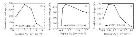
Fig.2. The breakdown voltage changes with doping concentration in drift region for(a)CON-LDMOS,(b)CON-SJLDMOS,and(c)VLW-LDMOS.
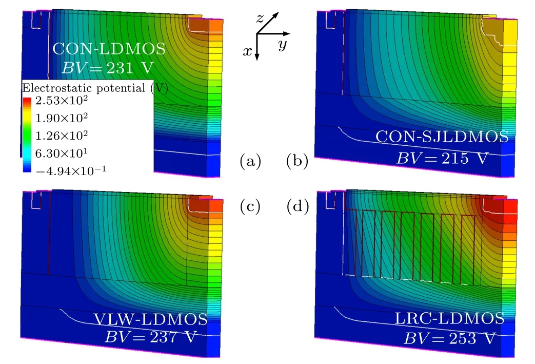
Fig. 3. Equi-potential contours and depletion layers for (a) conventional LDMOS,(b)conventional super-junction LDMOS,(c)VLW-LDMOS,and(d)LRC-LDMOS.
Figure 4 provides the surface, bulk, and bottom electric field distributions along the lateral direction for the devices. In Fig. 4(a), the surface peak electric fields Epeakof CON-LDMOS, CON-SJLDMOS, and VLW-LDMOS appear at the contact surface between the drain and N-drift region with values of 3.8×10⁵V/cm, 3.5×10⁵V/cm, and 2.9×10⁵V/cm, respectively. The surface Epeakwith value 3.4×10⁵V/cm of LRC-LDMOS appears at the P-body/Ndrift junction. Furthermore, the average electric field intensity of the entire N-drift region is enhanced because of the charge compensation between the LRC and the SJ. The bulk Epeakof the four devices at x = 1.0 µm is shown in Fig. 4(b), the Epeakof CON-LDMOS, CON-SJLDMOS,VLW-LDMOS, and LRC-LDMOS appear at the drain region with values of 3.4×10⁵V/cm,3.1×105V/cm,3.2×105V/cm,3.0×105V/cm,respectively.Moreover,the average bulk Epeakof LRC-LDMOS is much higher than that of the other three devices. The bulk Epeakof the four devices at x=3.0 µm is shown in Fig. 4(c), and the bottom Epeakat x=5.0 µm between the N-drift and the BOX is shown in Fig. 4(d). It can be seen that not only the average bulk electric distribution but also the bottom electric of the LRC-LDMOS are higher than that of the other three devices.
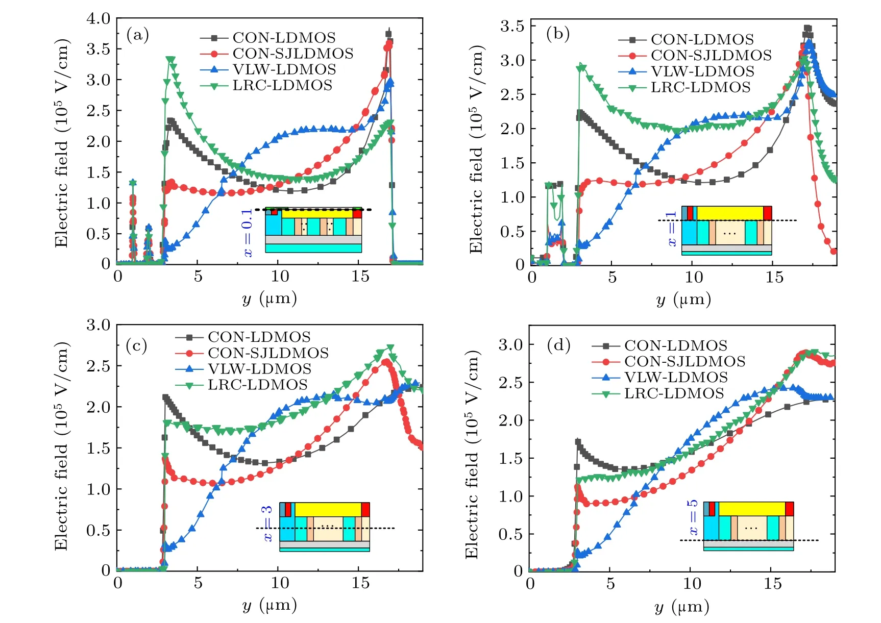
Fig.4. The surface,bulk,and bottom electric field distributions along the lateral direction for the CON-LDMOS,CON-SJLDMOS,VLW-LDMOS,and the LRC-LDMOS:(a)surface,x=0.1µm;(b)bulk,x=1.0µm;(c)bulk,x=3.0µm;(d)bottom,x=5.0µm.
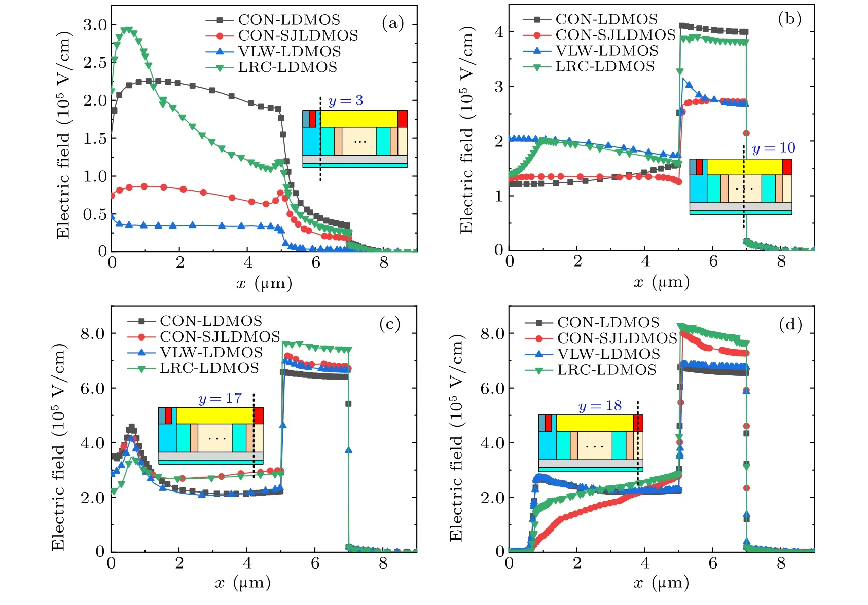
Fig.5. The electric field distributions along the vertical direction for the CON-LDMOS,CON-SJLDMOS,VLW-LDMOS,and the LRC-LDMOS at the cutline: (a)y=3µm,(b)y=10µm,(c)y=17µm,(d)y=18µm.
Figure 5 shows the the electric field distribution along the vertical direction of the devices. At the cutline y=3µm as shown in Fig. 5(a), the maximum Epeakis improved from 2.2×10⁵V/cm for CON-LDMOS to 2.9×10⁵V/cm for LRCLDMOS. At the cutline y = 10 µm as shown in Fig. 5(b),the Epeakin the drift region increased from 1.2×10⁵V/cm for CON-LDMOS, 1.3×10⁵V/cm for CON-SJLDMOS, and 2.0×10⁵V/cm for LRC-LDMOS to 2.0×10⁵V/cm for VLWLDMOS.At the cutline y=17µm as shown in Fig.5(c),the Epeakin the N-drift region of LRC-LDMOS is smaller than that of the other three devices. The electric field distribution at y=18 µm is shown in Fig. 5(d), it can be seen that the electric field at the drain of LRC-LDMOS is smaller than that of CON-LDMOS and VLW-LDMOS, and larger than that of CON-SJLDMOS.
3.2. Specific on resistance Ron,sp
Figure 6(a) shows the current voltage characteristics of the LDMOSs at forward conduction state. The source and the P-substrate are shorted to the ground, the gate electrode Vgis set at 10 V.The currents are increased linearly with the drain voltage for the devices,and the current of the LRC-LDMOS is significantly larger than the CON-LDMOS and VLW-LDMOS due to the LRC structure, which is basically equal to that of CON-SJLDMOS. Figure 6(b) shows the transfer characteristic curves of the devices, the threshold voltage Vthare almost 4.8 V.
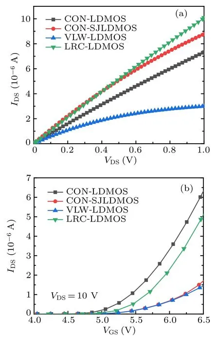
Fig.6. The I–V curve of the four LDMOSs: (a)forward conduction characteristic curve and(b)transfer characteristic curve.
Figure 7 shows the corresponding specific on resistance Ron,spof the LDMOSs at forward conduction state, it can be seen that the Ron,spof the LRC-LDMOS is much lower than the CON-LDMOS and VLW-LDMOS,which is basically equal to that of CON-SJLDMOS.
Figures 8 and 9 show the electron current density diagrams of the four devices. Combining with Figs. 8 and 9,it can be seen that the electron current density of the CONLDMOS is obviously lower than that of the other three structures, but there is electron current in the drift region of the CON-LDMOS. It can be seen from Figs. 8 and 9 that there is little difference in electron current density among CONSJLDMOS,VLW-LDMOS,and LRC-LDMOS,but their conductive regions are different.
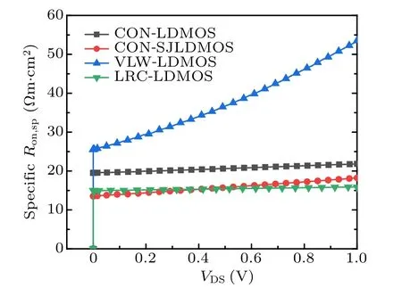
Fig.7. The specific on resistance Ron,sp of the LDMOSs.
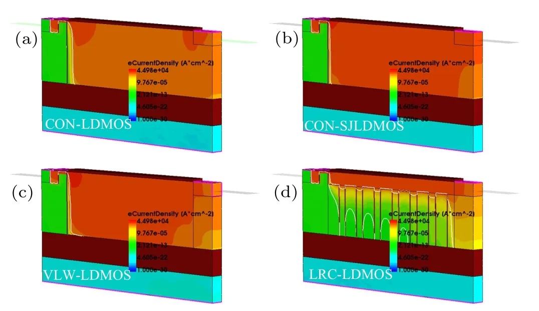
Fig.8.Electron current density(VGS=10 V,VDS=1 V),(a)CON-LDMOS,(b)CON-SJLDMOS,(c)VLW-LDMOS,(d)LRC-LDMOS.
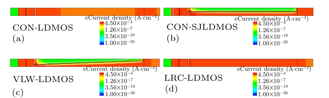
Fig.9.Cross section of electron current density(VGS=10 V,VDS=1 V),(a)CON-LDMOS,(b)CON-SJLDMOS,(c)VLW-LDMOS,(d)LRC-LDMOS.
3.3. Key parameters influence on BV and Ron,sp
Figure 10 shows the effect of the thickness Tcand doping concentration Ncof the low resistance electron channel on the BV and Ron,sp. In Figs. 10(a) and 10(b), the Ron,spis decreased linearly with the increase of Tcand Ncdue to the conduction capability of the LRC being enhanced. However,the BV is increased linearly and then decreased with the increase of Tcand Nc,it reaches the maximum value BV =253 V when Tc=1.0µm and Nc=1.0×1016cm−3.It is because the LRC should be completely depleted by the P-pillar,at the same time the charge compensation is satisfied between the N-pillar,LRC and P-pillar.

Fig.10. The BV and Ron,sp are functions of the low resistance electron channel for the LRC-LDOMS:(a)the thickness Tc of the low resistance electron channel and(b)the doping Nc of the low resistance electron channel.
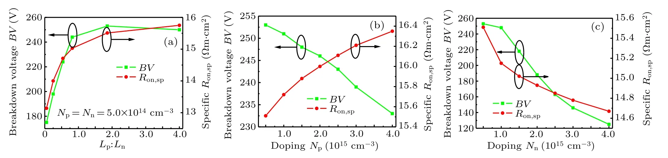
Fig.11. The BV and Ron,sp are functions of the N-pillar and P-pillar for the LRC-LDOMS(a)the length ratio Lp:Ln of the SJ,(b)the doping Np of the P-pillar,(c)the doping Nn of the N-pillar.
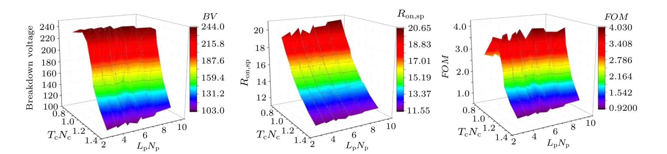
Fig.12. Effect of doping concentration and thickness of LRC and P-pillar on device performance: (a)breakdown voltage,(b)specific Ron,sp,and(c)FOM.
Figure 11 shows the influence of the width ratio and doping concentration of the SJ on BV and Ron,sp. The SJ under the LRC is divided into 7 sections. In Fig.11(a),the Ron,spis increased rapidly with the increase of Lp:Ln,and then it reaches almost saturation at Lp:Ln=1.85. The BV is optimized to a maximum value by adjusting the width ratio Lp:Ln=1.85 to satisfy the charge balance.Figure 11(b)shows that the Ron,spis increased gradually with the increase of Npof the P-pillar,and it is decreased gradually with the increase of Nnof the N-pillar as shown in Fig.11(c). However,the BV reaches its maximum value when the Npand Nnof super-junction concentration are 5.0×1014cm−3.
Figure 12 shows the breakdown voltage,Ron,spand FOM of the device when various parameters of LRC-LDMOS change.
3.4. Baliga’s figure of merit
Figure 13 shows the ideal silicon limit of the RESURF LDMOS given in Ref. [22] and the Ron,spversus the BV relationship of the LRC-LDMOS. It is apparent that the performance of the proposed LDMOS breaks through the silicon limit. The Table 1 shows the main performance parameters of LDMOS with the experimental and simulated data reported previously in Refs.[9,16,18]. The FOM (Baliga’s figure of merit)is defined as BV2/Ron,spto describe the trade-off performance of the devices. It can be seen that the FOM is 4.1 MW/cm2with the BV of 253 V and Ron,spof 15.5 mΩ·cm2for the LRC-LDMOS, compared the CON-LDMOS with 0.28 MW/cm2and the CON-SJLDMOS with 2.38 MW/cm2,the FOM is improved almost 146.4%and 172%,respectively.In addition, compared with VLW-LDMOS and CBSLOPLDMOS, the FOM of LRC-LDMOS has increased by 131%and 138%,respectively.
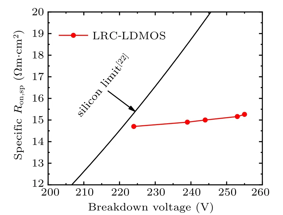
Fig.13. Specific Ron,sp versus BV relationship for the LDMOS device with the experimental and simulated data reported previously.
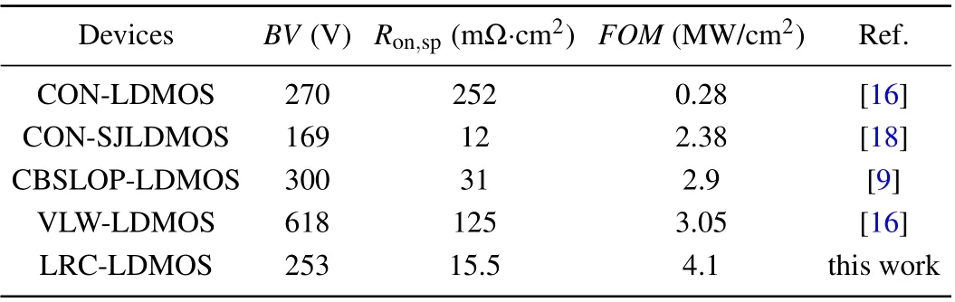
Table 1. BV,Ron,sp,and FOM of the proposed devices.
4. Conclusion and perspectives
A novel LRC-LDMOS with low resistance channel based on the SJ structure is proposed. The LRC is highly doped to provide an electron current channel at the forward conduction state, which significantly decreases the specific Ron,sp. The surface and bulk electric fields are modulated by adjusting the charge compensation between the LRC,N-pillar,and P-pillar,which obviously increases the BV.Finally the tradeoff performance of the LRC-LDMOS breaks through the ideal silicon limit with superior FOM.
猜你喜欢
Chinese Physics B(2022年11期)2022-11-21
Chinese Physics B(2022年4期)2022-04-12
Plasma Science and Technology(2022年2期)2022-03-10
疯狂英语·读写版(2021年5期)2021-06-15
武汉科技大学学报(社会科学版)(2020年2期)2020-04-28
杰出人物(2020年2期)2020-04-01
Chinese Physics B(2019年10期)2019-11-06
河北医科大学学报(2017年2期)2017-03-10
- Chinese Physics B的其它文章
- Corrosion behavior of high-level waste container materials Ti and Ti–Pd alloy under long-term gamma irradiation in Beishan groundwater*
- Degradation of β-Ga2O3 Schottky barrier diode under swift heavy ion irradiation*
- Influence of temperature and alloying elements on the threshold displacement energies in concentrated Ni–Fe–Cr alloys*
- Cathodic shift of onset potential on TiO2 nanorod arrays with significantly enhanced visible light photoactivity via nitrogen/cobalt co-implantation*
- Review on ionization and quenching mechanisms of Trichel pulse*
- Thermally induced band hybridization in bilayer-bilayer MoS2/WS2 heterostructure∗