
Black phosphorus junctions and their electrical and optoelectronic applications
2021-08-26 06:47NingqinDengHeTianJianZhangJinmingJianFanWuYangShenYiYangandTianLingRen
Journal of Semiconductors 2021年8期
关键词:诗经
Ningqin Deng, He Tian,, Jian Zhang Jinming Jian Fan Wu Yang Shen Yi Yangand Tian-Ling Ren
1Institute of Microelectronics, Tsinghua University, Beijing 100084, China
2Beijing National Research Center for Information Science and Technology (BNRist), Tsinghua University, Beijing 100084, China
3National Institute of Metrology (NIM), Beijing 100029, China
Abstract: Black phosphorus (BP), an emerging two-dimensional material, is considered a promising candidate for next-generation electronic and optoelectronic devices due to in-plane anisotropy, high mobility, and direct bandgap.However, BP devices face challenges due to their limited stability, photo-response speed, and detection range.To enhance BP with powerful electrical and optical performance, the BP heterostructures can be created.In this review, the state-of-the-art heterostructures and their electrical and optoelectronic applications based on black phosphorus are discussed.Five parts introduce the performance of BP-based devices, including black phosphorus sandwich structure by hBN with better stability and higher mobility,black phosphorus homojunction by dual-gate structure for optical applications, black phosphorus heterojunction with other 2D materials for faster photo-detection, black phosphorus heterojunction integration with 3D bulk material, and BP via Asdoping tunable bandgap enabling photo-detection up to 8.2 μm.Finally, we discuss the challenges and prospects for BP electrical and optical devices and applications.
Key words: black phosphorus; photodetector; heterostructure; homojunction; 2D material
1.Introduction
It is well known that the industry based on silicon faces many challenges due to the continuous scaling down the feature size[1−3].Therefore, breakthroughs in materials science play a significant role in the future development of technology and various applications.In 2004, graphene was the first discovered two-dimensional (2D) material extracted as a single layer of carbon atoms that are bonded together in a hexagonal honeycomb lattice from graphite[4].It had attracted worldwide attention owing to its unique properties, including ultra-high mobility[5]and thermal conductivity[6], transparency[7], and high Young's modulus[8].By virtue of their outstanding contribution to graphene development, the graphene discoverers, Konstantin Novoselov and Andre Geim, were awarded the Nobel Prize for physics in 2010.Devices based on graphene have shown various promising applications such as transistors[9−11], supercapacitors[12], batteries[13], solar cells[14], speakers[15,16], and thermal rectifiers[17],etc.In brief, graphene has blazed a new trail for developing 2D material and has a promising future from research laboratories to industrial applications.However, the on/off ratio of graphene transistors was limited to ~10 because of graphene’s vanishing bandgap.
Since graphene discovery, many kinds of 2D materials have been discovered and developed, such as hexagonal boron nitride (hBN)[18], elemental analogs of graphene[19], transition metal dichalcogenides (TMDCs), etc.Molybdenum disulfide (MoS2), one kind of transition metal dichalcogenide,has a bandgap.The bandgap of single-layer MoS2and the few layers MoS2are ~1.8 and ~1.2 eV, respectively[20].The on/off ratio field-effect transistors based on MoS2can reach~108, which is far beyond graphene devices’ performance[21].However, the relatively low charge carrier mobility at room temperature was a limitation for the applications of MoS2material.
Black phosphorus (BP) has a puckered structure that is one of the few-layered crystals and demonstrates strong inplane anisotropy.The phosphorus was first recorded in “The Book of Odes and Hymns” (诗经) that can be traced back to about three centuries ago in ancient China[22].However, the Nobel Prize in Physics was awarded to Percy Williams Bridgman who first synthesized BP until the twentieth century[23].With the development of exfoliation and thin-layer processing techniques, phosphorene (a single-layer BP) was exfoliated for the first time from bulk BP via the Scotch-tape method.BP is considered as a new member joining the two-dimensional material family[24−26].BP is a semiconductor with thickness-dependent direct bandgap and the bandgap of BP can be tuned continuously from ~0.3 eV (bulk) to ~2 eV (monolayer)[27], which is located between graphene and MoS2.It means that BP is a natural wide spectrum detection material and especially has a promising potential to have a breakthrough in mid-infrared applications[28].Besides, there are two distinct advantages for transistors based on BP becausethey balance the on/off ratio compared to graphene and MoS2[24,29−32].Furthermore, BP also has good thermal[33−36]and mechanical characteristics[37].In a word, BP, a new member in the family of 2D materials, has increasingly attracted substantial research interests and offers an opportunity to complement conventional silicon-based devices in various applications.

Fig.1.(Color online) Overview of BP crystal structure and BP devices.
In this review, as shown in Fig.1, we will introduce the BP sandwich structure with hBN, BP homojunction devices,BP heterojunction devices with other 2D and 3D bulk materials, and BP doped by As with tunable bandgap.There are three important issues (interface contact, interfacial modification and carrier separation) related to the BP electrical and optoelectronic devices.(1) For BP interface contact, different work-function metals can enable different transport behaviors.If Au or Ni is used, since the work function of Au is close to the middle of the bandgap of BP, so BP FET shows bipolar transport[29].If high work function metal Pd is used, BP FET shows more like a p-FET[53].If low work function metal Al is used for BP, n-FET is formed[102].Typically, there is a Fermi-pining effect between BP and contact, which needs further exploration for contact optimization.(2) BP suffers from stability issues[103].There is POxforming on both sides of BP[104].There are several ways to enhance the stability: hBN protection[61],AlOxprotection[105], and chemical protection[106].These methods are very efficient to enhance the stability of the BP film with long time.(3) For BP photodetectors, the carrier separation is the key to enable the photodetection.If the BP is intrinsic, the carrier separation can be speedy, but the photoresponsivity can be relatively low[81].For intrinsic BP with a perfect lattice structure, the electron–hole pair can be separated easily in BP based on the photovoltaic effect.Youngbloodet al.found the largest photocurrent produced underVG= –8 V with a high response bandwidth exceeding 3 GHz, which is related to the intrinsic region of BP under photovoltaic effect[81].The photo-gating effect cannot dominate in the above case because the trapping center is not enough in high-quality BP.Supposing the BP is doped by E-field or chemical and there is carrier trapping during the separation (i.e.photo-gating effect), in that case, the photoresponsivity can be very high, but the speed can be relatively low.For doped BP with enough trapping centers due to the degradation in air, the photo-gating effect can dominate the photo-sensing behaviors.Guoet al.reported high gain BP photodetectors based on the largest photocurrent produced at the BP doped region, which is related to the doped region of BP under the photo-gating effect[70].There is a trade-off between choosing high photoresponsivity and response-speed.

Fig.2.(Color online) Black phosphorus sandwich structure integration with hBN and its band structure.(a) A 3D schematic of hBN/BP/hBN heterostructure.(b) The HSE06 calculation results of the band structure and the local density of states (LDOS) for the hBN/BP heterostructure.Modified with permission from Ref.[38]Copyright 2016 American Chemical Society, (b) Ref.[39]Copyright 2015 American Chemical Society.
2.Black phosphorus sandwich structure with hBN
Hexagonal boron nitride is a large-bandgap and chemically stable two-dimensional dielectric material, usually forming a sandwich structure with black phosphorus (Fig.2(a)).As shown in Fig.2(b), density functional theory calculation shows that characters such as direct bandgap and linear dichroism are preserved when capping an hBN layer on to protect BP[39].Caiet al.concludes that hBN is a suitable material for capping BP, protecting it against structural and chemical degradation while still maintaining its major electronic characteristics.The hBN layers’ surface is smoother than SiO2and is free of dangling bonds and surface charge traps.Thus, hBN is widely used as a substrate to improve the transport properties of other 2D materials[40−44].
Combining the advantages of hBN, researchers have realized the hBN/BP/hBN structure to improve the transport properties and stability of BP (Fig.3(a)).Taoet al.calculated the physical properties of hBN/BP/hBN heterostructures with different hBN thicknesses[49].Compared with monolayer (ML)BP, the bandgap of the hBN(1ML)/BP(ML)/hBN(1ML) trilayer structure was increased by 0.15 eV.However, when the thickness of hBN continuously increased, the bandgap of BP had little change.They also observed an increased hole and electron effective masses via increasing hBN thickness.Doganovet al.compared mobilities of different substrate dielectrics of BP-based FET as a function of temperature, including BP/SiO2,BP/hBN, and hBN/BP/hBN.These results show that the hBN substrate improves mobility compared with SiO2due to the higher dielectric constant.Furthermore, the full encapsulation with hBN increased the mobility over 100 cm2/(V·s) as shown in Fig.3(b)[45].Geimet al.assembled hBN/BP/hBN heterostructure using the dry transfer method in an inert atmosphere.They used monolayer or bilayer hBN on top of BP to protect it from all gases and liquids, and the top hBN layer can let electrons tunnel through, so the electrical contacts can be evaporated onto it without etching openings in the encapsulation.They achieved field-effect mobility of over 4000 cm2/(V·s) for bulklike devices (>10 layers) and about 1200 cm2/(V·s) in a trilayer device (Fig.3(c)).Moreover, it also showed long-term stability according to the experimental electrical results stored in the air.Quantum oscillations were observed in hBN/BP/hBN sandwiched structures[46].Nathanielet al.fabricated the structure with one-dimensional edge contact to metal electrodes.As temperature decreased, the transistor behaved as a gate-dependent metal–insulator transition and device mobility increased.AtT= 1.5 K, the mobility reached as high as 4000 cm2/(V·s).Under the condition of moderate magnetic fields and low temperature, they observed gate-tunable Shubnikov de Haas (SdH) magneto-oscillations and Zeeman splitting with an estimatedg-factor ~2[32].Xiaolonget al.used a high-temperature annealing process to reduce the charge trap density in BP.They realized high field-effect mobility of 1350 cm2/(V·s) at room temperature and higher mobility of 2700 cm2/(V·s) atT= 1.7 K.Meanwhile, they observed quantum oscillations and zero Berry phase at the suitable magnetic field and low temperature[30].
Quantum Hall (QH) effect was observed in hBN/BP/hBN two-dimensional electron systems (2DES).Likaiet al.improved mobility of the system by placing the hBN-encapsulated BP on a graphite back gate.The graphite gate results in a high carrier Hall mobility up to 6000 cm2/(V·s) at temperaturesT< 30 K.The high mobility enabled them to observe the integer QH effect in BP.QH plateaus were observed at integer filling factorsνfrom 1 to 7[50].Longet al.measured hole mobility of the hBN/BP/hBN field-effect transistor on SiO2/Si substrate.The mobility was 5200 cm2/(V·s) at room temperature, and increased to 45 000 cm2/(V·s) at cryogenic temperatures (Fig.3(d)).They observed QH plateaus at ν from 2 to 12 (Fig.3(e))[47].Chenet al.reported a systematic study for thin-layer BP-based hBN/BP/hBN structure.They achieved the high intrinsic saturation velocity of holes and electrons at room temperature.As shown in Fig.3(f), the FET and Hall mobilities can reach up to 3388 and 2024 cm2/(V·s), respectively[48].In order to compare the transport properties of black phosphorus BP and BP heterostructures, we list mobilities and on/off ratio for various BP and BP-related heterostructures at different experimental temperatures in Table 1.Most of the BP devices show mobility less than 1000 cm2/(V·s),while the hBN/BP/hBN sandwich structures show the improved mobility larger than 1000 cm2/(V·s).There is strong evidence that the hBN/BP/hBN can enhance the mobility.
3.Black phosphorus homojunction by dual-gate structure
The p–n junction is a fundamental building block for the realization of incumbent electronic and optoelectronic devices.In conventional semiconductors, substitutional doping is commonly used to gain n- or p-type characteristics.BP,an ambipolar 2D material, can form n–n, n–p, p–n, and p–pjunctions by doping or combining with other 2D materials such as hBN or graphene, respectively.Buscemaet al.fabricated p–n junctions based on 2D materials, namely, hBN and BP, which are gate dielectric and channel material, respectively.They observed photovoltaic properties and the detection wavelength up to the near-infrared.Meanwhile, the transfer curves can be turned into four operational quadrants by different gate voltages (Fig.4)[65].Liuet al.reported a controllable doping technique using Al atoms to realize a high-performance photovoltaic device, which enhanced 2.5 times electron mobility.The open-circuit voltage responsivity and a short-circuit current responsivity reached ~15.7 × 10³V/W and ~6.2 mA/W at room temperature in the near-infrared(1550 nm), respectively[60].Hanet al.demonstrated that the electron mobility of BP could be increased one order of magnitude through in situ functionalization of potassium[59].Recently, Tianet al.reported 2D junctions made of BP and graphene whose type of device can be controlled by the back gate and graphene gate[66].BP is regarded as a promising material for high speed, high response, and comprehensive spectrum detection from visible to mid-IR at room temperature.

Fig.3.(Color online) Fabrication process and mobility of hBN/BP/hBN heterostructure devices.(a) A 3D schematic of hBN/BP/hBN heterostructure device fabrication process.(b) Mobility results of the different structures including BP/SiO2 (red), BP/hBN (green), and hBN/BP/hBN (blue).(c)Mobility results of the trilayer and 20-layer were measured at liquid helium temperatures.(d) Mobility as a function of temperature for different carrier densities were measured.(e) Quantum Hall states with filling factors from 2 to 12 are observed.(f) FET and Hall mobilities at different temperature.Modified with permission from (a) Ref.[30]Copyright Nature publishing group, (b) Ref.[45]Copyright AIP Publishing, (c) Ref.[46]Copyright 2015 American Chemical Society, (d) and (e) Ref.[47]Copyright 2016 American Chemical Society, (f) Ref.[48]Copyright 2018 American Chemical Society.

Table 1.Comparison of performance of FETs based on BP and BP heterostructures, including BP film thickness, structure, mobility, on/off ratio.

Fig.4.(Color online) Drain current mapping and band diagrams of the few-layer black phosphorus PN junction.Drain current mapping at(a) + 100 mV and (b) –100 mV as a function of Vrg and VIg, respectively.(c) Schematic energy band diagrams of the different device configurations.Modified with permission from Ref.[65]Copyright 2014 Springer Nature.
4.Black phosphorus heterojunction with other 2D materials (graphene, MoS2, etc.)
In the conventional p–n homojunction, the p- and n-type regions are formed by chemically doping a bulk semiconductor depleted of free charge carriers, creating built-in potentials.However, 2D semiconductors like BP, graphene, and transition metal dichalcogenides (TMDCs) can stack, forming their unique van der Waals (vdW) structures, which are predicted to exhibit utterly different charge transport characteristics than bulk heterojunctions.The novel bulk crystals are composed of individual layers, in which the van der Waals forces vertically stack each layer instead of covalent bonds.Because of their particular structures, they have great potential for the next-generation electronic and optoelectronic applications[77−79].BP could stack with other 2D materials to form heterojunctions that reveal unusual properties and new phenomena.
4.1.Graphene and black phosphorus
Two-dimensional materials such as graphene have exhibited excellent optical characteristics and offer an attractive prospect for next-generation optoelectronics applications.Graphene has been used for the wideband photodetection from ultraviolet to terahertz[80].However, graphene photodetectors' dark current is very high due to the graphene lack ofa bandgap.Youngbloodet al.fabricated a gated multilayer black phosphorus photodetector.The device's dark current is only 220 nA (VG= −8 V,Vbias= −0.4 V).Moreover, the intrinsic responsivity can reach up to 135 and 657 mA/W in 11.5-nm- and 100-nm-thick devices at room temperature, respectively.In almost all aspects of their performance, BP photodetectors are superior to graphene photodetectors[81].Huet al.fabricated a 2D hybrid phosphorene and graphene nanocomposite (Fig.5(a)) and calculated the electronic bandgap using HSE06 method (Fig.5(b)).The results show that the Fermi velocity of graphene at the Dirac point is kept and open a small bandgap (58 meV), which shows field-effect transistors'potential graphene/BP heterojunction[82].Avsaret al.realized vertical field-effect transistors (VFETs) based on graphene/BP van der Waals heterostructure, which achieved an on/off ratio of ~100 at room temperature (Fig.5(c))[61].Kanget al.realized an on/off ratio of over 800 at 30 K and high on-state current densities of over 1600 A/cm2in graphene/BP VFETs(Fig.5(d))[64].Besides, BP/graphene composite has a widely attracted ion battery research field due to the highest theoretical capacity of phosphorus, high electronic conductivity, mechanical strength, and fast reaction kinetics of graphene[83−86].

Fig.5.(Color online) Bandgap and structure of graphene/BP heterojunction.(a) The top and side views of schematics of BP (violet)/graphene(gray) heterojunction.(b) The HSE06 calculation results of the band structure are graphene, phosphorene and graphene/BP heterojunction, respectively.(c) Transfer characteristic curves for an encapsulated device by measuring under both vacuum and ambient conditions.The inset shows a nonencapsulated device test.(d) Transfer characteristic curves at ranging various temperatures from 300 to 30 K in 30 K steps.Modified with permission from (a) and (b) Ref.[82]Copyright Royal Society of Chemistry, (c) Ref.[61]Copyright 2015 American Chemical Society, (d) Ref.[64]Copyright 2016 American Chemical Society.
4.2.TMDCs and black phosphorus
TMDCs are atomically thin two-dimensional semiconductors of the type MX2.M is a transition metal atom (Mo, Re,etc.) and X is a chalcogen atom (S, Se, etc.).Molybdenum disulfide (MoS2) is the most exciting material in the TMDCs owing to its robustness[87].MoS2has been reported in the research of photodetectors due to unique optoelectronic properties[88−90].BP-based optoelectronic devices are also widely researched, especially in the advantages of the near-infrared and infrared bands due to the lattice structure and band structure of BP[67−71].Denget al.designed a gate-tunable p–n diode based on a p-type BP/n-type monolayer MoS2van der Waals p–n heterojunction which is the first 2D heterostructure demonstrated using black phosphorus.In the experiments, monolayer MoS2was synthesized by chemical vapor deposition (CVD) on 285 nm SiO2/p+-doped Si substrate, and the BP was mechanically exfoliated on the monolayer MoS2.The thicknesses of the few-layer BP flake and monolayer MoS2are 11 and 0.9 nm, respectively.The diodes based on 2D materials achieved a maximum photodetection responsivity of 418 mA/W and photovoltaic energy generation with an external quantum efficiency of 0.3% under the illumination of 633 nm He–Ne laser[72].Taking advantage of BP bandgap in the infrared, Yeet al.fabricated a diode based on BP/MoS2heterojunction as shown in Fig.6(a).It realized microsecond response speed ~15μs, which is 2 to 3 orders higher than that of the BP-based non-heterojunction photodetector in the near-infrared (Fig.6(b))[74].Kwaket al.performed a BP/WS2heterojunction device at 405 nm and solar spectrum.The extern-al quantum efficiency and the photovoltaic efficiencies are 4.4% and 4.6%, respectively, which shows potential for photovoltaic applications[91].In addition to combining two materials, the structure's heterojunction has also been reported.Liet al.realized a bipolar phototransistor based on WSe2/BP/MoS2heterostructure (Fig.6(c)).As shown in Fig.6(d), a broadband detector has a high responsivity of 6.32 A/W at visible light and 1.12 A/W at the infrared light, respectively[75].The value of the photoresponsivity is an order of magnitude higher than that of the detector based on the WSe2/BP heterostructure.Besides, Srivastavaet al.fabricated a BP/rhenium disulfide (ReS2) broken-gap van der Waals heterojunction device as shown in Fig.6(e).Its photoresponsivity and the maximum external quantum efficiency (EQE) can reach up to 8 mA/W(Fig.6(f)) and 0.3% under illustration under the illumination of 532 nm laser[76].

Fig.6.(Color online) The photodetectors based on TMDCs/BP heterojunctions.(a) A 3D schematic of the BP/MoS2 heterojunction device.(b)On/off switching characteristics of the BP/MoS2 junction device under illumination of 1.55 μm laser (Laser power 96.2 μW) at different bias voltages.The rise time and the decay were 15 μs and 70 μs, respectively.(c) A 3D schematic of the WSe2/BP/MoS2 heterojunction device.(d)Photoresponsivity and photogain of the WSe2/BP/MoS2 heterojunction device as a function of wavelength, respectively.(e) A 3D schematic diagram of the ReS2/BP heterojunction device.(f) Current rectifying output characteristics as a function of incident laser power values under illumination of 532 nm laser.Modified with permission from (a) and (b) Ref.[74]Copyright 2016 American Chemical Society, (c) and (d) Ref.[75]Copyright 2017 American Chemical Society, (e) and (f) Ref.[76]Copyright 2019 American Chemical Society.
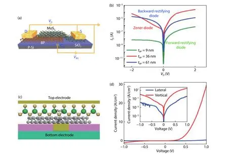
Fig.7.(Color online) Structure and performance of the lateral and vertical BP/MoS2 heterostructures.(a) A 3D schematic of the BP/MoS2 heterojunction device.(b) The diode current (Id) as a function of the voltage across the diode at different thicknesses of BP which are 9, 36 and 61 nm, respectively.(c) A schematic diagram of the BP/MoS2 heterostructure device cross-section.(d) I–V characteristics of vertical and lateral BP/MoS2 heterojunction diodes.The inset shows semilogarithmic scale plot of the same I–V curves.Modified with permission from (a) and (b) Ref.[63]Copyright 2017 American Chemical Society, (c) and (d) Ref.[92]Copyright 2017 American Chemical Society.
Depending on the carrier transport path, the FET structure based on vdW heterostructures is mainly divided into two categories: lateral heterojunction structure and vertical heterojunction structure.In a lateral heterojunction, the"edge-to-edge" structure allows carriers to conduct primaries in the material plane.However, the "up–down" structure allows carriers to conduct primarily between layers of material for a vertical heterojunction.Xuet al.fabricated a tunneling field-effect transistor based on a BP/MoS2junction.The device's subthreshold swing (SS) values were ~65 and 51 mV/dec at room temperature and 160 K, respectively[62].For vertical heterojunctions, they are mainly used for vertical field-effect transistors.This type of device's implementation is mainly due to the excellent quality interlayer conductivity of the two-dimensional semiconductor material.Liuet al.realized a BP/MoS2tunneling heterojunction diode (Fig.7(a)).They observed three kinds of diode characteristics, including a backward rectifying diode, a Zener diode, and a forward rectifying diode tuned by the thickness of BP (Fig.7(b))[63].Miaoet al.realized a truly vertical p–n heterojunction diode based on MoS2/BP heterojunction (Fig.7(c)).The p–n junction of the vertical structure exhibits a higher on current density than that of the lateral p–n junction.Moreover, they used MoS2to isolate the effects of air increasing device lifetime(Fig.7(d))[92].A comparison of photodetectors based on BP and BP heterostructures is listed in Table 2.The BP/MoS2heterojunction device shows a faster photo-response speed down to 15μs than BP FETs around 1 ms.
5.Black phosphorus heterojunction with 3D bulk material
The 2D material can be combined with 3D bulk material to form a new heterojunction due to their atomic thin body thickness and the lack of dangling bonds on the surfaces.The integration of 2D material with bulk material can also promote industry applications.The mixed-dimensional 2D/3D vdW heterostructures can improve optical absorption crosssections than all-2D vdW heterostructures[93].Gehringet al.transferred a thin-layer BP (~15 nm) sheet onto Te-doped GaAs substrate to form a heterojunction.The maximum EQE of the device can reach 9.7% under the illumination of 514 nm laser at zero bias (Fig.8(a)) and be increased to 31% at a bias of –2.5 V[94].Besides, 2D–3D p–n heterojunctions can become easily doped and have a high breakdown electric field for field-effect devices.Liet al.reported a vdW heterojunction JFET based on p-type BP and n-typeβ-Ga2O3.It exhibits excellent rectification characteristics and low reverse current in the order of picoamperes.Moreover, the source–drain current switching ratio can reach 107(Fig.8(b))[96].Biet al.realized two kinds of structures: tunnel field-effect transistor(TFET) and junction field-effect transistor (JFET) via the integration of InGaZnO and BP.The TFET’s current switching ratio achieved over 105, and the device's SS values was about 11 mV/dec.Meanwhile in BP/InGaZnO heterostructure JFET, italso shows on/off ratio over 105, almost no hysteresis and larger SS of 83 mV/dec due to the limitation of thermal emission (Fig.8(c))[109].

Table 2.Comparison of performance of photodetectors based on BP and BP-related heterostructures, including film thickness, structure, spectral range, responsivity, specific detectivity and response time.

Fig.8.(Color online) Performance of BP/ 3D bulk material heterojunction device.(a) EQE as a function of laser power for different laser light wavelengths at zero source–drain bias based on BP/GaAs heterojunction.(b) Semi-log plot of the transfer characteristics of the JFET based on BP/β-Ga2O3 heterojunction.(c) The transfer characteristics of BP/InGaZnO JFET.The inset shows the corresponding μFE value.Modified with permission from (a) Ref.[94]Copyright AIP publishing, (b) Ref.[96]Copyright 2020 IOP, (c) Ref.[109]Copyright 2020 John Wiley and Sons.
6.BP doped by As with tunable bandgap
Black phosphorus doped by arsenic or black arsenic–phosphorus (b-AsP), a family of layered semiconductors, has attracted extensive attention due to the excellent tunability of bandgaps.Liuet al.demonstrated the bandgap could be tuned to 0.15 eV smaller than BP (0.3 eV).It means that the detection range of the photodetectors based on b-AsP can reach the long-wavelength infrared (LWIR) (Figs.9(a) and 9(b))[95].Longet al.fabricated long-wavelength IR, the detection range up to 8.2μm, photodetectors based on b-AsP.They achieved fast photoresponse (0.54 ms) tested in the mid-wavelength infrared, as shown in Fig.9(c).Furthermore,this type of device had low dark noise at room temperature whose peak specific detectivity value can reach up to 9.2 ×10⁹Jones (Fig.9(d))[97].B-AsP can also be combined with hBN to form a sandwich structure the same as BP.Yuanet al.fabricated a photodetector based on hBN/b-As0.83P0.17/hBN structure, which achieved good responsivity in the mid-infrared.Moreover, the air stability of the type of device enhanced owing to the hBN encapsulation[98].
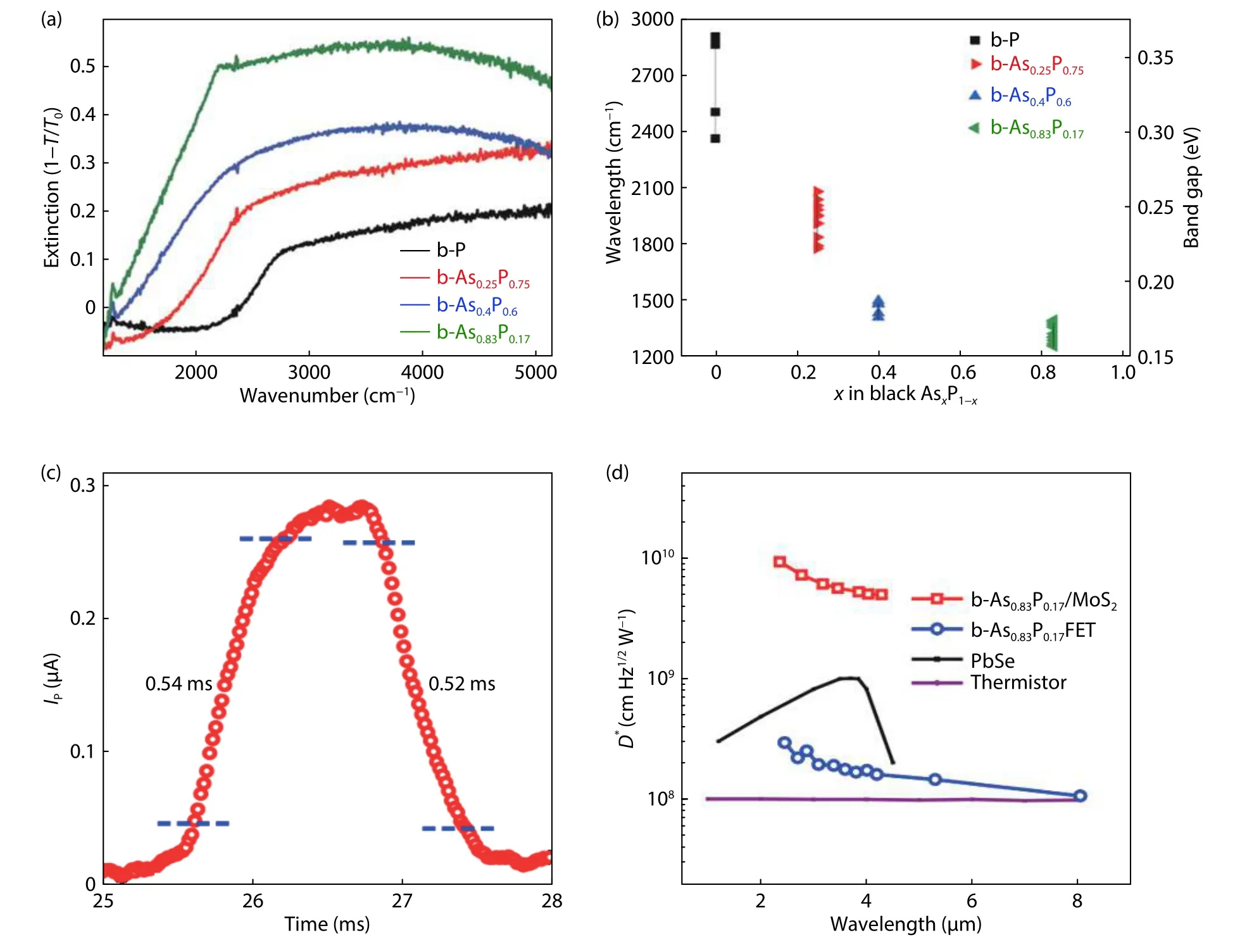
Fig.9.(Color online) Performance of the related b-AsP photodetectors.(a) Infrared absorption as a function of wavenumber for different samples including b-P, b-As0.25P0.75, b-As0.4P0.6 and b-As0.83P0.17, respectively.(b) Bandgap and wavelength as a function of different composition-tunable b-AsxP1−x or different polarization angle of the same composition, respectively.(c) Response curve as a function of time under illumination of 4.034 μm of the b-AsP photodetector.(d) Specific detectivity of different detectors as a function of wavelength including a thermistor bolometer, a PbSe detector, a b-AsP FET device and a b-AsP/MoS2 heterostructure.Modified with permission from (a) and (b) Ref.[95]Copyright John Wiley and Sons, (c) and (d) Ref.[97]Copyright AAAS.
7.Summary and perspectives
In this review, heterostructures based on BP and their electrical and optical applications were discussed in detail.With the tremendous development of applications based on BP owing to its superior characteristics, an increasing number of novel devices based on BP broadly potential from laboratory research to practical use.To achieve this goal, researchers have to suffer from several challenging problems in further research and some possible solutions for dealing with the challenges as follows.(1) Synthesize high-quality wafer-scale crystalline and controllable thicknesses of BP.Fabrication of controllable thicknesses of BP with high quality is essential to design the BP-based devices and applications due to the thickness-dependent intrinsic direct bandgap.Most recently, Xuet al.show the large-area of BP grown on insulating silicon substrates by a gas-phase growth method[107].It is promising to use the gas-phase growth method for wafer-scale BP.Until now, wafer-scale BP films have not been produced, which greatly hinder the BP-based large-scale applications.(2) Enhancement of long-term stability for BP-based device.Although many strategies have been attempted to improve BP devices' long-term stability, including functionalization, doping, and passivation, the experimental results still show a long distance with commercial grade products.To enhance the long-term stability for BP-based devices for commercialgrade products, a vacuum package can be considered.(3)The BP-based integrated circuits.The complementary inverter is the fundamental building block for logic circuits.Some BP-based complementary inverters have been fabricated via the adatom doping technique[68,99,100]or BP hybrids[101].The uniformity of BP devices is still required to enable large-scale integrated circuits.The MoS21-bit microprocessor has been done[108].The BP-based integrated circuits should come true soon, right after obtaining the wafer-scale BP film.If the large-scale BP can be obtained, there is also a great potential to enable an array of BP photodetectors for middle-IR photodetection at room temperature, which could be better than the commercial HgCdTe middle-IR photo-detectors.Moreover, the high mobility and reasonable on/off ratio of the BPFET can enable next-generation flexible electronics and circuits with high performance, which is better than the organicbased flexible electronics.
Acknowledgements
This work was supported in part by Fundamental Research Project of National Institute of Metrology China under Grant AKYZZ2116, in part by National Natural Science Foundation of China under Grant 62022047, Grant 61874065 and Grant 51861145202, in part by the National Key R&D Program under Grant 2016YFA0200400, in part by the Research Fund from Beijing Innovation Center for Future Chip and the Independent Research Program of Tsinghua University under Grant 20193080047, in part by Young Elite Scientists Sponsorship Program by CAST under Grant 2018QNRC001, and in part by Fok Ying-Tong Education Foundation under Grant 171051.
猜你喜欢
意林彩版(2022年2期)2022-05-03
今日中国·西班牙文版(2020年11期)2020-11-06
学生天地(2020年12期)2020-08-25
学生天地(2020年7期)2020-08-25
天津诗人(2019年4期)2019-11-27
诗歌月刊(2019年7期)2019-08-29
诗歌月刊(2019年8期)2019-08-22
中国三峡(2017年1期)2017-06-09
中华诗词(2017年10期)2017-04-18
火花(2015年8期)2015-02-27
 Journal of Semiconductors2021年8期
- Journal of Semiconductors的其它文章
- Polymer acceptors for all-polymer solar cells
- Ionic liquids in perovskite solar cells
- Perovskite crystallization
- All-polymer solar cells
- Ultraviolet communication technique and its application
- Extensive study of optical contrast between bulk and nanoscale transition metal dichalcogenide semiconductors