
Design,fabrication,and characterization of Ti/Au transition-edge sensor with different dimensions of suspended beams
2021-11-23 07:31HongJunZhang张宏俊JiWen文继ZhaoHongMo莫钊洪HongRuiLiu刘鸿瑞
Chinese Physics B 2021年11期
Hong-Jun Zhang(张宏俊), Ji Wen(文继), Zhao-Hong Mo(莫钊洪), Hong-Rui Liu(刘鸿瑞),
Xiao-Dong Wang(汪小东)1, Zhong-Hua Xiong(熊忠华)1, Jin-Wen Zhang(张锦文)2,3,†, and Mao-Bing Shuai(帅茂兵)1,‡
1Institute of Materials,China Academy of Engineering Physics,Mianyang 621000,China
2Institute of Microelectronics,Peking University,Beijing 100871,China
3National Key Laboratory of Micro/Nano Fabrication Technology,Institute of Microelectronics,Peking University,Beijing 100871,China
Keywords: transition-edge sensor,Ti/Au,superconductivity film,microfabrication,deformation of suspended structure
1. Introduction
The transition-edge sensor (TES) is a microcalorimeter operating in correspondence of the superconducting-to-normal transition region and weakly coupled to a cold bath. TES can be adapted for detecting THz, IR, VIS, UV, x-ray, andγray radiation by measuring the temperature variation after photon absorption.[1]Over the past decade,the TES microcalorimeter has become fundamental in applications such as high-energy astrophysics, nuclear science and biophysics, astronomy, and quantum information.[2-5]
Superconducting transition sensors are thermal detectors relying on the steep resistive transition of a superconducting material as a thermometer. Ti-based superconducting thin films are principal semiconductor materials for TES because of their low superconducting transition temperature and compatibility with micromachining. The superconducting transition temperature can be reduced by adding a layer of normal metal to it. Although single-layer Ti[6]and other Tibased bilayers, such as Ti/Pd,[7]Ti/TiN,[8]and Ti/Al,[9]have been studied because of the excellent electrical conductivity, thermal conductivity, and chemical inertia of Au, Ti/Au bilayers are the principal materials for TES research on Ti substrates. Ti/Au bilayers are prepared by sputtering,[10-13]electron beam evaporation,[14-17]and the combination of the two processes.[18]The heat capacity of the substrate can be reduced by placing superconducting films on the suspended membranes of low-stress Si3N4. Moreover, different suspended film processes have been developed. These processes are predominantly based on(100)Si substrate dry deep etching[7,13,19]or dry wet combination processes[20,21]to remove the Si substrate and obtain a suspended structure. Moreover,the wet etching of(110)silicon substrate is used to obtain vertical sidewalls.[20]To reduce the thermal noise further,the primary structure of the Ti/Au/Si3N4suspension membrane is supported using Si3N4suspended beams. In 1999,Kiewiet[15]proposed a new suspended structure,called spiderweb,with a diameter of 1.4 mm and supported by 16 legs of 0.55 mm long,5 µm wide, and 1 µm thick. The suspended beam was improved from a wider double-end fixed support[11]to narrower four corner beams, and its width was reduced to 5 µm[20]or even<1µm.[21]Khosropanah[22]developed the ultimate spiral folded structure to increase the length of beams. Although low-stress Si3N4is used as the support structure,the deformation of the suspended structure will be caused by stress mismatch between the superconducting bilayer and metallic Pb,and the suspended beam will aggravate the deformation,[19]which will inevitably affect the mechanical stability,yield,and reliability of the device. However,few observations and analysis of Ti/Au morphology and structure deformation exist.
In this study, Ti-/Au-based TES devices with different suspended structures were designed, and the thickness ratio was maintained at 1:1. Firstly, the structure realizability of TES devices with different size of cantilever beams was experimentally explored. Secondly, the effects of different size of cantilever beams and processing technology on the morphology of suspended films were experimentally studied, which laid the foundation for the reliability and consistency of devices. Finally,the effects of structure and morphology on the thermal response and low temperature characteristics of devices were measured and studied, and then the effects on the TES characteristics. In this paper, we focused on the measurement and analysis of the processing technology and the morphology and roughness of the suspended structure. In the future, we will measure the thermal response and low temperature characteristics of these structures and analyze their effects on the TES characteristics. Direct current (DC) magnetron sputtering combined with dry wet etching was used to fabricate the suspended Ti/Au TES structure. Scanning electron microscopy (SEM), energy-dispersive spectroscopy(EDS),and atomic force microscope AFM measured the composition and surface morphology of Ti/Au. The deformation of different suspended structures was observed and analyzed using a laser confocal microscope. Moreover, using a semiconductor parameter analyzer, theI-Vcharacteristics of different TES devices were evaluated and compared under the four-lead and two-lead resistance measurement methods. Finally,the low-temperature superconductivity of Ti/Au TES devices was confirmed using a dilution refrigeration device.
2. Design and fabrication
The thermal insulation ability of Ti/Au bilayers can be improved by selecting materials with lower thermal conductivity as weak thermal bonding. Compared with other common microelectronic processing materials, Si3N4has lower thermal conductivity (2-155 W/(m·K)). Because the suspension structure should have good mechanical properties, low stress Si3N4thin films with a thickness of 500 nm are selected as weak thermal bonding materials. Figure 1 shows the structure of the Ti/Au TES device. Four cantilevers distributed at four corners support the Si3N4film suspended in the center.The square Ti/Au bilayer on the suspended Si3N4film is a TES sensor. Four Si3N4cantilever beams are covered with Al as electrode leads. Ti/Au TES devices with different areas are designed, including 75 µm×75 µm, 150 µm×150 µm,200 µm×200 µm, and 300 µm×300 µm. Their supporting beams are 100 µm long and 25 µm wide. Furthermore,Si3N4beams with different widths and lengths are designed to analyze the influence of beam geometry on deformation and resistance. When the beam width is fixed at 25µm,the beam length is 50, 100, 200, 400, and 600 µm; however, when the beam length is fixed at 100 µm, the beam width is 10, 15,25,30,and 40µm. All TES sizes are compared with the suspended and non-suspended structures, and the resistances are measured using four-lead and two-lead arrangements to compare the deformation and electrical characteristics.
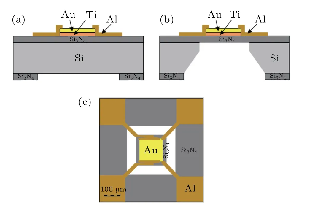
Fig.1. Schematic of Ti/Au TES devices. Panel(a)shows the vertical profile of the TES device. The Si substrate below is unetched,and the Ti/Au bilayer is in a non-suspended state. Panel (b) shows the vertical profile of the TES device with a suspended structure. Based on the non-suspended structure,Si substrate under the Ti/Au bilayer is etched to form a suspended structure.Panel(c)shows the top view of the TES device with a suspended structure.The white part is a hollow structure. The Si3N4 film suspended in the center is supported by four cantilevers distributed at four corners. The square Ti/Au bilayer on the suspended Si3N4 film is a TES sensor. Four Si3N4 cantilever beams are covered with Al as electrode leads.
Figure 2 schematically shows the principal processing steps for TES fabrication. The TESs are manufactured on four-inch diameter,400-µm-thick〈100〉,double-side polished Si wafers. Firstly, stoichiometric silicon nitride layers with a thickness of 500 nm are deposited on both sides of the silicon wafer using low-pressure chemical vapor deposition(LPCVD)(Fig.2(a)). Secondly,the Si3N4layer on the back is patterned via reactive ion etching (RIE) (Fig. 2(b)). Thirdly, two layers of Ti and Au with the same thickness of 25 nm are continuously deposited in turn using DC magnetron sputtering(Fig. 2(c)). By adjusting the appropriate deposition conditions, the films with good surface roughness and low stress can be obtained.[23,24]The thickness of the bilayer is carefully selected to achieve a suitable superconducting transition temperature.[25]Fourthly, lithography and wet etching steps are used to pattern the bilayer (Fig. 2(d)). Fifthly, a layer of Al with a thickness of 300 nm is sputtered and patterned via a lift-off process (Fig. 2(e)). Sixthly, the Si on the backside is etched to a depth of 385µm with KOH solution(Fig.2(f)).Finally,the remaining 15-µm-thick silicon is etched out using anisotropic Si etch (ASE) to form a Si3N4suspended membrane(Fig.2(g)).
Ti/Au TESs with different structures are successfully fabricated as per the design. Figure 3(a) shows the front optical image of the TES.The length and width of the beam are 50µm and 25µm,respectively,and the Ti/Au area of the suspended structure is 150µm×150µm.Figures 3(b)and 3(c)show significant deformations in the TES,where the beams are slightly concaved and the Ti/Au bilayer convexed mildly. Therefore,the deformations of devices with different structural parameters must be comprehensively characterized and analyzed.Figure 3(d)shows the TES photo of the prepared 4×4 arrays.All pixels are completely suspended and the structure is intact.
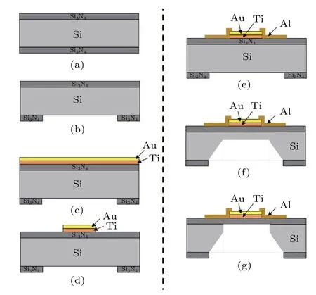
Fig. 2. The principal processing steps for TES fabrication. (a) First, stoichiometric silicon nitride layers with a thickness of 500 nm are deposited on both sides of the silicon wafer using low-pressure chemical vapor deposition(LPCVD).(b)Second,the Si3N4 layer on the back is patterned using reactive ion etching(RIE).(c)Third,two layers of Ti and Au with the same thickness of 25 nm are continuously deposited in turn using DC magnetron sputtering.The thickness of the bilayer is carefully selected to achieve a suitable superconducting transition temperature. (d) Fourth, lithography and wet etching steps are used to pattern the bilayer. (e)Fifth,a layer of Al with a thickness of 300 nm is sputtered and patterned via a lift-off process. (f)Sixth,the Si on the backside is etched to a depth of 385µm using KOH solution. (g)Finally,the remaining 15-µm-thick Si is etched out by anisotropic Si etch(ASE)to form a Si3N4 suspended membrane.
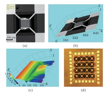
Fig.3. Images of the TES.Panel(a)shows the front optical image of TES.The length and width of the beam are 50µm and 25 µm, respectively, and the Ti/Au area of the suspended structure is 150 µm×150 µm. Panels (b)and (c) show significant deformations of the TES. The beams are slightly concaved,and the Ti/Au bilayer mildly convexed. Panel(d)shows the TES photo of the prepared 4×4 arrays. All the pixels are completely suspended,and the structure is intact.
3. Results and discussion
3.1. Morphology and components of the Ti/Au bilayer
The surface topography and element compositions of the grown Ti/Au bilayer are characterized by performing SEM and EDS, and the results are presented in Figs. 4(a) and 4(b), respectively. Grains on the surface have good homogeneity,and their sizes are distributed between 15 nm and 86 nm.The EDS spectrum in Fig.4(b)shows that Ti and Au are the two dominant elements,in addition to the wafer material silicon.
Figure 5 shows the cross-section morphology of the Ti/Au bilayer obtained using SEM.The thickness of the Si3N4layer deposited by LPCVD is 539.5 nm,which is close to the desired thickness of 500 nm. Moreover,the thickness of the Ti/Au bilayer is 41.6 nm, which is close to the desired thickness of 50 nm.
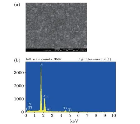
Fig.4. Analysis results of the Ti/Au bilayer obtained using SEM.Panel(a)shows the surface morphology of the Ti/Au bilayer. Grains on the surface have good homogeneity,and their sizes distribute between 15 nm and 86 nm.Panel(b)shows the EDS spectra of the Ti/Au bilayer. Ti and Au are the two dominant elements,in addition to the wafer material silicon.

Fig.5. Cross-section morphology of the Ti/Au bilayer obtained using SEM.
The surface morphology of TES is characterized using the Olympus LEXT OLS 4500 scanning probe microscope(SPM)in various stages of TES preparation. Firstly, the Si substrate and low-stress stoichiometric Si nitride surfaces deposited by LPCVD are measured and observed. Figure 6(a) shows that the surface roughness of the Si substrate is 0.151 nm,indicating that the average height fluctuation of the double polished Si wafer surface is of the order of 1 ˚A.Figure 6(b)shows that the surface roughness of low-stress Si3N4is 0.934 nm. Compared with the Si substrate, the increase in roughness is< 1 nm,which can be ignored compared with the thickness of 500 nm of Si3N4. The surface roughness of Ti/Au films prepared by sputtering is 1.601 nm,which increases further compared with that before growth.Both the silicon nitride growth process and the Ti/Au film-sputtering process can significantly increase the surface roughness.However,compared with the film thickness of 50 nm,the surface roughness of 1.601 nm is acceptable.
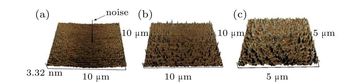
Fig.6.The surface topography by Olympus LEXT OLS 4500 scanning probe microscope (SPM). Panel (a) shows the surface topography of the doublesided polished silicon wafer. Panel(b)shows the surface topography of the non-suspended Ti/Au bilayer.
3.2. Morphology and components of the Ti/Au bilayer
Laser confocal microscopy(LCM)is used to observe the 3D morphology of TES with suspended structure, and the height difference between the culmination of the suspended film and the wafer reference plane is measured. Figure 7 shows the structure pattern of TES. The directionO →Bis vertical to the metal electrode,and the directionO →Ais parallel to the metal electrode. As all Ti/Au bilayers mildly arch,the center of the bilayer is the culmination, and the edge of the bilayer is the bottom. The altitude differences between the culmination and bottom with the reference plane referring to the wafer are measured both vertically and horizontally, respectively. Figure 7 shows that the altitude difference between the pointsOandAand the pointsOandBrefers to the altitude difference of the culmination with the reference plane horizontally and vertically,respectively. Similarly,the altitude difference between the pointsCandD, and the pointsEandFrefers to the altitude difference of the bottom with the reference plane horizontally and vertically,respectively.

Fig. 7. The microscopy photo and height measurement diagram of Ti/Au TES.
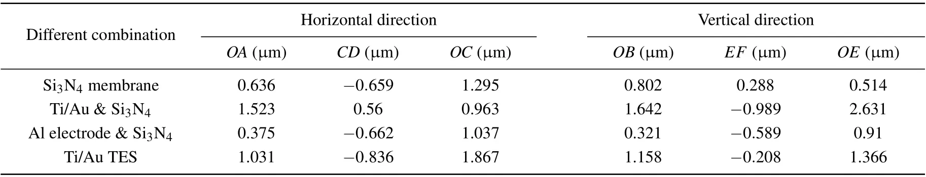
Table 1. Influence of the Ti/Au bilayer and Al electrode on the deformations of TES.
The Ti/Au bilayer and Al electrode on the deformations of TES are evaluated by measuring the deformation of four suspended structures, including Si3N4, Ti/Au/Si3N4, Al/Si3N4,and Ti/Au/Si3N4with an Al electrode. Table 1 shows the results of deformations. Slight deformations occur in every direction on the Si3N4membrane with a suspended structure because of the stress of materials. The deformation effect of the Ti/Au bilayer is greater than that of the Al electrode.Vertically,the altitude differences between the point O and the point E on the suspended Si3N4film-deposited Ti/Au bilayer and Al electrode are 2.631 µm and 0.91 µm, respectively. However,the altitude difference vertically becomes 1.366µm after both the Ti/Au bilayer and the Al electrode have been deposited in turn. The reason for this phenomenon is that the action directions of Al and Ti/Au bilayers on Si3N4vertically is opposite such that the deformation of the TES film vertically becomes smaller. Similarly, horizontally, the depositions of the Ti/Au bilayer and Al electrode on the suspended Si3N4film present the altitude difference of 0.963 µm and 1.037 µm, respectively,and the result becomes 1.867µm when both the Ti/Au bilayer and Al electrode have been deposited. The reason for the larger deformation of TES horizontally could be that the stress action direction of the Ti/Au bilayer and Al electrode on Si3N4is the same such that they overlap, increasing the deformation of TES horizontally.
Next,the influence of the cantilever beam size on the deformation of suspended TES is analyzed. Firstly, the lengths of the cantilever beams are changed with the width of the beams and the size of the suspended membrane are fixed at 25µm and 150µm×150µm,respectively. Table 2 shows the results of the deformations of the TES using different beam lengths. Vertically and horizontally,with the increase in beam length,the change rule of height difference between the highest and lowest points of the membrane is not obvious. However,the shorter the beam length is,the smaller the device deformation is.Similarly,Table 3 shows the influence of cantilever beams with different widths on the deformation of the suspended TES.The widths of the beams and size of the suspended membrane are fixed at 100µm and 150µm×150µm,respectively.Table 3 shows that the height differences between the vertex pointOand the edge points of the membrane decrease with the increase in beamwidth. Table 3 shows the same trend that the height differences betweenOAandOBdecrease with the increase in beamwidth. Hence,the wider the width of the cantilever beam is, the smoother the TES is and the lower the stress is.

Table 2. Influence to the deformations of TES with different beam length.

Table 3. Influence on the deformations of the TES with different beam widths.

Table 4. Influence on the deformations of the TES with different dimensions of the Ti/Au bilayer.
Furthermore,the deformation of TES in different areas of the Ti/Au bilayer is analyzed when the length and width of the cantilever beam are fixed at 100µm and 25µm,respectively.
Table 4 shows that with the increase in the film area,the height differences between the vertex pointOand the other edge points increases. Because the increase in the film area might enlarge the deformation of TES to some extent, the height difference is converted into the radius of curvature for comparison (Table 5). Table 5 shows that the larger the area of the Ti/Au bilayer is, the larger the curvature radius of the suspended film is. Therefore, the relative deformation of the TES is lesser with the area increase in the Ti/Au bilayer.
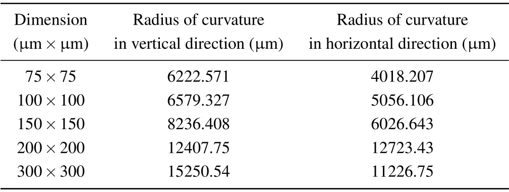
Table 5. Values of the radius of curvature under different dimensions of the Ti/Au bilayer.
3.3. Measurement and analysis of electrical characteristics
The electrical characteristics of TES are characterized by conducting four-lead[26]and two-lead electrical transport measurements. The resistance test instrument is an HP 4156b semiconductor parameter analyzer combined with an MM probe station. The current scanning range is−1 mA to+1 mA, and the scanning step is 10 µA. The resistance obtained from the four-lead arrangement denotes the resistanceRTESof the TES.The resistanceR2−leadobtained from the twolead arrangement is the sum of the contact resistanceRcont,the lead resistanceRlead,and theRTES.
The effect of the suspended structure on the electrical properties of TES is evaluated by measuring the resistances of the Ti/Au bilayer for suspended and non-suspended,respectively.The size of the suspended film is fixed at 150×150µm.The lengths of the beam with the same width of 25µm are 50,400, and 600 µm, respectively. Figure 8 and Table 6 show theI-Vcurves of the TES obtained using the four-lead and two-lead arrangements,respectively.
Table 6 shows that the resistances measured using the four-lead arrangement are similar in the case of the suspended and non-suspended structures. Although significant TES deformations with suspended structure are observed, the results show that the suspended structure has less influence on the resistanceRTESof TES.The difference in the resistancesR2−leadmeasured using the two-lead arrangement is small,indicating that suspended or not has little influence on the resistances of lead and contact. Furthermore, the sum of the contact resistancesRcontand lead resistancesRleadcan be calculated usingRTESandR2−lead(Table 6).RTESandR2−leadvary with the size of the beam and suspended film. With increase in cantilever beam length,the resistanceR2−leadcorrespondingly increases.

Fig.8. The I-V curves of the TES.Panel(a)shows the results from the fourlead arrangement.Panel(b)shows the results from the two-lead arrangement.
3.4. Superconductivity measurement
Figure 9 shows the inside of the Leiden MNK-126-450 dilution refrigeration(DR).It provides a low-temperature environment for testing superconductivity. The resistance is measured using the AVS-47B AC electric bridge. The sizes of the Ti/Au bilayer and the Si3N4beam are 150µm×150µm and 100µm×25µm,respectively.
The transition temperature of superconductivity is related to the Fermi surface topology.[27]Figure 10(a) shows the results of the resistance-temperature curve of the suspended TES. Figure 10(b) shows that the transition temperature is 253 mK,which is close to that reported in Ref.[1].The normal resistanceRnormalof the Ti/Au bilayer is 1.12 Ω,and 10%and 90%ofRnormalare selected as the lower and upper limits of the superconducting transition width, respectively. Accordingly,the temperature transition region is[249 mK,255 mK],and the transition width is 6 mK.The sensitivity,α,for a detector can be described asα= d(lnR)/d(lnT).[28]Figure 10(b) shows that the linearity of d(lnR) and d(lnT) is good. The relationship between the resistance and temperature in the normal logarithm form can be expressed as lnR=95.1×lnT −527.2.Thus,the temperature sensitivityαis 95.1.

Fig.9. Image of the Leiden MNK-126-450 DR.
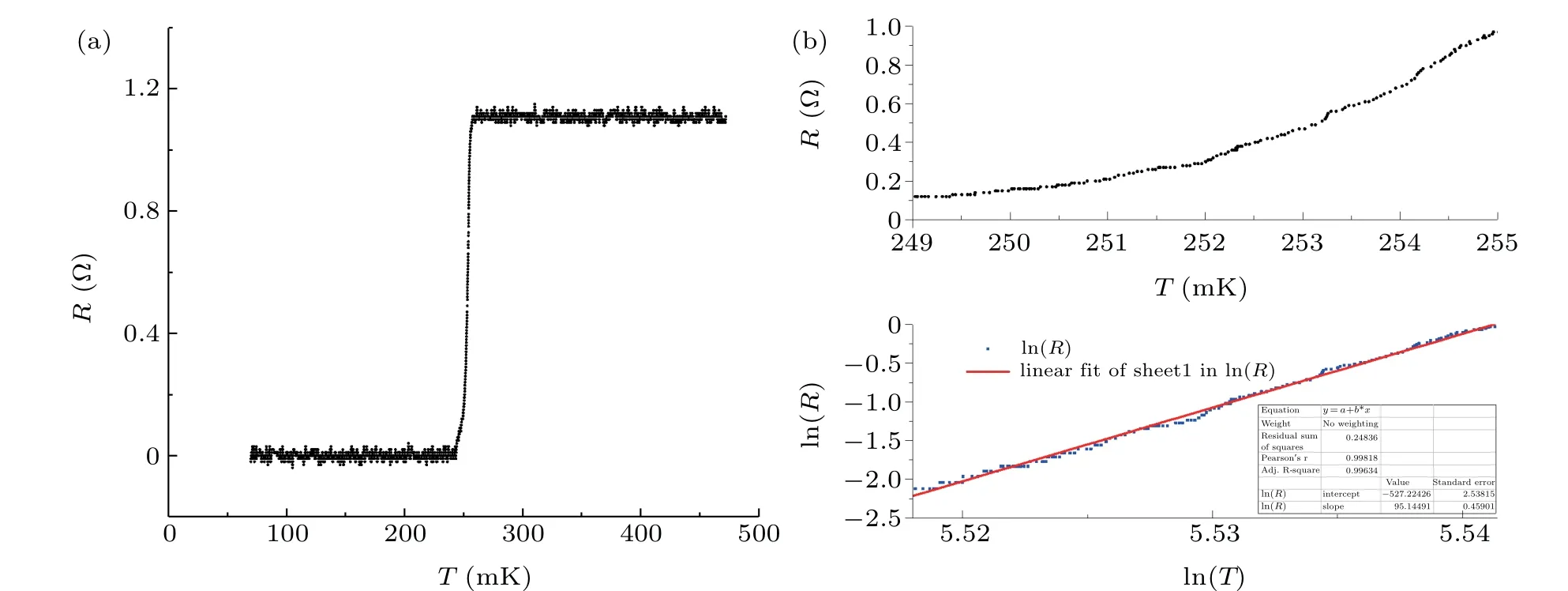
Fig. 10. The superconductivity of the Ti/Au bilayer. The sizes of the Ti/Au bilayer and Si3N4 beam are 150 µm×150 µm and 100 µm×25 µm,respectively. Panel(a)shows the curve of R-T. The superconducting transition temperature is 253 mK.The normal resistance Rnormal of the Ti/Au bilayer is 1.12 Ω. Panel(b)shows the details of the superconducting transition process. The transition width is 6 mK.
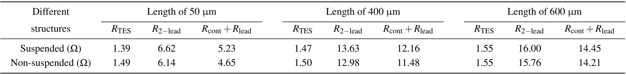
Table 6. The resistance of TES with different structures of TES.
4. Conclusion
In this study,Ti/Au TES devices with different suspended structures were designed and fabricated using micromachining. The properties of TES were measured and compared,including surface morphology,the 3D deformation of the suspended structure,I-Vcharacteristics,and low-temperature superconductivity. Compared with the surface of the Si substrate, the surface roughness of low-stress Si3N4and Ti/Au bilayers was significantly increased; however, they were still within an acceptable range,and the quality of the bilayer was good. The TES device with a suspended low-stress Si3N4film had a slight deformation. The sputtering Al electrode had a limited effect on the deformation of the TES device. The deformation of the TES device was predominantly attributed to the Ti/Au bilayer.The shorter the beam length was,the smaller the device deformation was, and the wider the support beam was,the smoother the suspended film was. As the area of the suspended Si3N4film increased,the curvature radius increased and the deformation decreased. The resistance of TES devices with different structures was~1.68 Ω whether suspended or not. With increase in beam length or decrease in beamwidth,the resistance of the TES device increased. The superconducting critical transition temperature was 253 mK, with a width of~6 mK and the value of the temperature sensitivityαwas 95.1. In the future,the thermal response and low temperature characteristics of these structures will be measured, and the effects of morphology and stress on the characteristics of TES devices will be discussed in detail.

- Chinese Physics B的其它文章
- Numerical investigation on threading dislocation bending with InAs/GaAs quantum dots*
- Connes distance of 2D harmonic oscillators in quantum phase space*
- Effect of external electric field on the terahertz transmission characteristics of electrolyte solutions*
- Classical-field description of Bose-Einstein condensation of parallel light in a nonlinear optical cavity*
- Dense coding capacity in correlated noisy channels with weak measurement*
- Probability density and oscillating period of magnetopolaron in parabolic quantum dot in the presence of Rashba effect and temperature*