
Magnetic two-dimensional van der Waals materials for spintronic devices*
2021-11-23 07:32YuZhang张雨HongjunXu许洪军JiafengFeng丰家峰HaoWu吴昊GuoqiangYu于国强andXiufengHan韩秀峰
Chinese Physics B 2021年11期
Yu Zhang(张雨) Hongjun Xu(许洪军) Jiafeng Feng(丰家峰) Hao Wu(吴昊)Guoqiang Yu(于国强) and Xiufeng Han(韩秀峰)
1Beijing National Laboratory for Condensed Matter Physics,Institute of Physics,Chinese Academy of Sciences,Beijing 100190,China
2Center of Materials Science and Optoelectronics Engineering,University of Chinese Academy of Sciences,Beijing 100049,China
3Songshan Lake Materials Laboratory,Dongguan 523808,China
Keywords: magnetic two-dimensional van der Waals materials,spintronic devices
1. Introduction
Two-dimensional (2D) van der Waals (vdWs) material refers to a layered system,where a single atomic layer or several atomic layers are stacked by vdWs force bonding. The research field of 2D materials has grown rapidly since the successful exfoliation of the single-layer graphene in 2004.[1]The intriguing properties of graphene have inspired researchers from different research areas to explore the emerging phenomena in the 2D systems,and,to date,huge amounts of novel 2D vdWs materials have been proposed and discovered. The 2D vdWs materials have also attracted special attention from the spintronics community due to their prominent properties of 2D spin transport. For example,graphene-like materials that consist of light elements have a long spin lifetime and a long spin diffusion length, which make them a perfect spin transport medium. The transition metal dichalcogenides (TMDs) with strong spin-orbit coupling serve as a new platform for spincharge interconversion and interplay with other pseudo spins(like valley spintronics). Moreover,integrating 2D vdWs materials into spintronic devices allows adding exotic functionalities,such as the gate-,pressure-,and strain-tunability,[2-7]mechanical flexibility,[8]and even new functionalities,i.e.,stacking order or twist angle-dependent properties.[9-11]Although there have been many types of 2D vdWs materials, including semiconductors, metals, insulators, superconductors, and topological insulators, one of the most critical pieces of the jigsaw puzzle, i.e., the intrinsic long-range magnetism, was still missing before 2016.
According to the Mermin-Wagner theorem,[12]the longrange magnetic order is dynamically unstable in the 2D limits. It was predicted that the strong thermal fluctuations inhibit the long-range magnetic order by exciting spin waves. Fortunately, a magnetic anisotropy can induce an energy gap for the spin wave in low dimensional systems and thus forbid the spin wave excitation, which allows stabilizing the long-range magnetic order in the 2D materials.[13]In 2016, the first evidence of the stable atomically-thin magnetic vdWs material was revealed by the Raman spectrum in FePS3crystals.[14,15]Subsequently, Gonget al.and Huanget al.found the direct evidence of spontaneous magnetization in single-layer Cr2Ge2Te6and CrI3by magnetooptic Kerr effect (MOKE), respectively.[13,16]The experimental results of Cr2Ge2Te6and CrI3support the intrinsic long-range magnetic order in the vdWs systems at the 2D limit. Since then, a great number of magnetic vdWs materials, including ferromagnetic (FM) and antiferromagnetic(AFM) materials, have been studied from bothab initiocalculations and the experiments. The typical 2D FM materials include Cr2X2Te6(X= Si, Ge, Sn),[13,17,18]FexGeTe2(x=3,4,5),[2,19-21]CrBr3,[22]1T-CrX2(X=S,Se,Te),[23-27]MX2(M=Mn, V;X=Se, Te),[28-31]PtSe2,[32,33]etc.; the typical 2D AFM materials include CrX3(X= Cl, I),[16,34]MPS3(M= Cr, Ni, Fe, Mn),[14,35,36]MnBi2Te4,[37]etc.Moreover, other complex magnetic structures, such as helical magnetism,[38]topological magnetic structure, multiferroics,spin glass,and frustrated magnetism,have also been reported in the 2D vdWs systems, enriching the family of the magnetic vdWs systems. The representative magnetic vdWs materials, which have been demonstrated in experiments, are summarized in Table 1.[20,21,23,26-29,33,39-49]It is worth mentioning that, in addition to the intrinsic magnetism, orbital magnetism was also reported in some nonmagnetic TMD materials. Sonet al. demonstrated that monolayer MoS2can generate valley orbital magnetization under an in-plane electric field due to the symmetry broken induced Berry curvature dipole.[50]Subsequently, Qinet al. realized orbital magnetization in monolayer WSe2via applying uniaxial strain and electric field.[51]
Table 1. Representative vdWs magnetic materials which have been demonstrated in experiments.
There are several methods for preparing 2D magnetic materials, such as growing single-crystal bulk materials combining with mechanical exfoliation to obtain atomically thin flakes, molecular-beam epitaxy (MBE), and chemical vapor deposition (CVD). These methods can be divided into two categories: top to down methods and bottom to up methods.The mechanical exfoliation method was initially used to obtain 2D magnetic vdWs materials by taking advantage of the weak vdWs force between layers.[13,16]Feiet al.[19]further adopted the Au-assisted mechanical exfoliation method to obtain thinner and larger Fe3GeTe2crystals. Denget al.[2]further developed this method by changing Au into Al2O3, and obtained monolayer Fe3GeTe2. Nevertheless, the traditional mechanical exfoliation method is very difficult to obtain largearea thin 2D magnetic materials, which limits the application of 2D magnetic materials. The MBE and CVD have also been adopted to grow 2D magnetic materials on a large scale. For example,monolayer Fe3GeTe2and Cr2Te3can be synthesized by using the MBE method.[52,53]At the same time, Cr2Te3,Cr2S3,and other materials were also synthesized by the CVD method.[54,55]
The discovery of magnetic vdWs materials seamlessly introduces a spin degree of freedom to conventional vdWs materials,which provides new material options for the development of spintronic devices. It is of importance to look back to the progress in this emerging research area and give an outlook to future research. We point out that there have been a few reviews, which mainly focus on the study of magnetic properties of 2D materials.[8,39,56-58]In this review,we provide an overview of recent experimental progress on the 2D magnetic materials and focus more on their applications in spintronic devices. This review includes three parts. In the first part,we focus on recalling the studies on the control of the 2D ferromagnetism. The attempts of 2D magnetic materials in spintronic devices are then reviewed. At last, we give an outlook to the future direction in this research area.
2. Control of 2D magnetic materials

Fig.1. (a)Crystal structure(side and top views)of Cr2Ge2Te6. (b)Optical image of exfoliated Cr2Ge2Te6 atomic layers and the emergence of a Kerr rotation signal for the bilayer.[13] (c)View of the in-plane(out-of-plane)atomic lattice of a single CrI3 layer. (d)Layer-dependent magnetic ordering revealed by Kerr rotation in atomically thin CrI3.[16] (a),(b)Reprinted with permission from Ref.[13]. Copyright 2017,Springer Nature.(c),(d)Reprinted with permission from Ref.[16]. Copyright 2017,Springer Nature.

Fig.2. (a)Schematic of a dual-gated bilayer CrI3 device. (b)Gate-induced transition from layered AFM to FM states at different magnetic field.[62](c) MCD versus magnetic field at 4 K at representative gate voltages.[63] (d) The schematic of the Fe3GeTe2 device structure and longitudinal conductance as a function of the gate voltage Vg measured in a Fe3GeTe2 device. (e)Phase diagram of the Fe3GeTe2 sample as the gate voltage and temperature are varied.(f)Rxy of a FGT flake under a gate voltage.[2](g)Schematic of the Fe3GeTe2 Hall-bar device gated by proton.(h)Gate-tuned ferromagnetism in Fe3GeTe2 nanoflake.[67](a),(b)Reprinted with permission from Ref.[62]. Copyright 2018,Springer Nature. (c)Reprinted with permission from Ref.[63]. Copyright 2018,Springer Nature. (d)-(f)Reprinted with permission from Ref.[2]. Copyright 2018,Springer Nature.(g),(h)Reprinted with permission from Ref.[67]. Copyright 2020,American Physical Society.
The pioneering studies on the direct observation of magnetic properties were performed on Cr2Ge2Te6and CrI3.[13,16]Cr2Ge2Te6is a vdWs FM material, and its crystal structure is shown in Fig. 1(a). The magnetism of Cr2Ge2Te6can be described by a 2D Heisenberg model with perpendicular magnetic anisotropy, and the Curie temperature (TC)of the bulk material is~61 K. It was found that its magnetic order remains in the bilayer Cr2Ge2Te6with a lowerTC(~22 K in Fig. 1(b)). Different from Cr2Ge2Te6,CrI3(crystal structure shown in Fig. 1(c)) is an A-type AFM material, which possesses the FM intralayer coupling(odd layers) and the AFM interlayer coupling (even layers). Therefore, the net magnetism of a CrI3flake depends on the number of layers (Fig. 1(d)). Cr2Ge2Te6and CrI3are semiconductors, and therefore their carrier concentration can be relatively easily tuned by the electric field.[59-64]More interestingly, it was found that the AFM coupling between layers of CrI3can be tuned through electrostatic doping.[62-64]Schematic diagram of the device is shown in Fig. 2(a) (Note that the dual-gate structure enables the electric field effect and the carrier doping effect independently). It can be seen from Figs.2(b)and 2(c)that the mutual transformation between the AFM state and the FM state of the bilayer CrI3can be achieved by adjusting the gate voltage(with the assistant of an external magnetic field). In addition to conventional electrostatic doping, ionic liquid gating can significantly enhance the electric field effect and even change the transport properties of metals. Denget al.[2]used the ionic liquid gating method for metallic Fe3GeTe2(as shown in Fig. 2(d)), and the electron doping of about 1014cm−2magnitude in each layer was realized, which can increase theTCof Fe3GeTe2to room temperature. As shown in Fig. 2(f),the Fe3GeTe2remains in a FM state up to 310 K after a gating voltage of 2.1 V is applied. This phenomenon was explained by the change of the density of states at the Fermi level of Fe3GeTe2.Compared to ionic liquid gating,the proton doping technique was developed recently, which may relieve the structure change or chemical reaction of ionic liquid gating by producing a similar doping level.[65,66]Zhenget al.[67]found that the proton doping produces a strong exchange coupling between adjacent layers in Fe3GeTe2(see Figs.2(g)and 2(h)). It can be seen from Fig. 2(h) that the gating voltage has a significant modulation on the coercivity field (Hc) of Fe3GeTe2,and a rarely seen zero-field cooled exchanged bias was achieved at the same time.
Because of the atomic thickness and the weak coupling between different layers, the structure and property of vdWs materials can be controlled by strain. Qiuet al. reported that patterned µm-size Fe3GeTe2shows the vortex domain structure at room temperature, which was ascribed to the straininduced effect by patterning(Figs.3(a)and 3(b)). The authors suggested that the vortex domain structure at room temperature is induced by the finite size effect or the Ga+ions injection during the fabrication process.[68]Wanget al.realized the adjustment of coercivity andTCof Fe3GeTe2through the selfmade strain test platform, as shown in Fig. 3(c). A dramatic increase ofHcby more than 150%was observed with a strain of 0.32%. Meanwhile, itsTCincreased almost linearly with the stress, rising from 180 K to 210 K (Fig. 3(d)). Density functional theory calculation results suggested that a highly symmetrical Fe3GeTe2bulk structure could undergo transitions with broken structural symmetries when the strain is applied,which contributes to the enhancement ofTC.[7]Besides the FM system,a strain-modulated AFM system was also reported. Niet al. observed that the N´eel vector could be tuned by the in-plane strain in atomically thin MnPSe3.[69]As shown in Figs. 3(e) and 3(f), the N´eel vector in MnPSe3is roughly along the nodal direction of the two-fold crossed pattern of the second-harmonic generation,which is controlled by the strain along different directions,e.g.,0°and 90°with respect to thexaxis. In fact, in atomically thin MnPSe3, the N´eel vector could be rotated to any in-plane direction by the strain,which is due to the strain-locked Ising order. Songet al. and Liet al. reported the static pressure tuning of the magnetic order in the 2D magnet CrI3.[4,5]And the interlayer coupling in CrI3was modulated from AFM to FM by applying a pressure of 2.7 GPa(Fig.3(g)). In addition to the above-mentioned studies, optical injection, chemical doping, dielectric regulation,and proximity effect were also employed to tune the magnetic properties of the magnetic vdWs system, such as it has been demonstrated that magnetic vdWs materials are susceptible to external stimulus manifesting the interface engineering for structures and properties adjustments. For the atomicallythick vdWs systems, it is actually a double-edged sword that might bring controllability but lose stability at the same time.

Fig. 3. (a) Enhanced TC in Fe3GeTe2 and its corresponding magnetic domain structures by pattern-induced strain. (b) Schematic diagram of a device in the strain adjustment experimental.[68] (c)Phase diagram of Fe3GeTe2 with temperature and strain involved. (d)A schematic of the method to control the in-plane strain.[7] (e)A schematic of the in-plane AFM N´eel order and second-harmonic generation measurement on MnPSe3. (f)N´eel vector in MnPSe3,which is close to the nodal direction of the two-fold crossed pattern of second-harmonic generation,was controlled by the strain along different directions,e.g., 0° and 90° with respect to the x axis.[69] (g)Magnetization tuned by pressure.[4] (a),(b)Reprinted with permission from Ref.[68]. Copyright 2018,American Chemical Society. (c), (d) Reprinted with permission from Ref. [7]. Copyright 2020, John Wiley and Sons. (e), (f) Reprinted with permission from Ref.[69]. Copyright 2021,Springer Nature. (g)Reprinted with permission from Ref.[4]. Copyright 2019,Springer Nature.
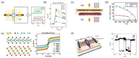
Fig.4. (a)Emergence of exchange bias in CrCl3/Fe3GeTe2 bilayer and(b)the exchange bias modulated by the thickness of CrCl3.[70](c)Magnetic ordering in vdWs Fe3GeTe2 and FePS3 thin flakes;(d)extracted Kerr rotations as a function of the temperature for Fe3GeTe2 (red curve)and FePS3/Fe3GeTe2 (blue curve), respectively.[73] (e) Geometric structure diagram and anomalous Hall resistance at different temperatures of Bi2Te3/Fe3GeTe2 heterostructure.[75](f) Schematic of a three-terminal spin valve measurement geometry and independent switching of the MCo and MCrSBr (and so MGr) under an external magnetic field.[76] (a),(b)Reprinted with permission from Ref.[70]. Copyright 2020,American Chemical Society. (c),(d)Reprinted with permission from Ref.[73]. Copyright 2020,John Wiley and Sons. (e)Reprinted with permission from Ref.[75]. Copyright 2020,American Chemical Society. (f)Reprinted with permission from Ref.[76]. Copyright 2021,Springer Nature.
Since the layered 2D vdWs materials are binding together by the vdWs force, different (magnetic) vdWs materials can be integrated with each other without the lattice mismatching issue. Therefore, heterostructures based on (magnetic)vdWs materials provide a platform with tremendous opportunities which might emerge unique performances and novel physical mechanisms. For example, FM vdWs can be combined with various AFM materials. Zhuet al.[70]prepared CrCl3/Fe3GeTe2heterostructures,and the exchange bias-field of 50 mT at 2.5 K was achieved (Fig. 4(a)). The magnitude of exchange bias can also be modulated by the thickness of CrCl3(Fig. 4(b)). Huet al.[71]used the same approach to construct the MnPS3/Fe3GeTe2device, in which,besides the exchange bias, they observed an anti-symmetric magnetoresistance. Zhanget al.[72]used vacuum exfoliation approach to prepared Fe3GeTe2/IrMn heterostructure, which achieved an exchange bias-field up to 895 Oe. Zhanget al.[73]reported the increase ofTCof Fe3GeTe2from 150 K to 180 K(Fig.4(d))while realizing the exchange bias by utilizing the interface proximity-effect in the Fe3GeTe2/FePS3heterostructure(Fig.4(c)). Interestingly,except the combination of FM material and AFM material elevatesTC, the combination of vdWs FM material with traditional AFM material achieves a similar effect. Idzuchiet al.[74]constructed a Cr2Ge2Te6/NiO heterostructure with a significant increase ofTCof Cr2Ge2Te6after the deposition of NiO.With the thickness of NiO increasing to 50 nm, theTCof Cr2Ge2Te6can reach up to 115 K,which almost doubles compared to the bare Cr2Ge2Te6. In addition to the FM/AFM bilayer heterostructure, the heterostructure formed by magnetic vdWs materials and topological insulators(TI),graphene,and other vdWs materials also show unique properties. Wanget al. used MBE to grow the Bi2Te3/Fe3GeTe2heterostructure, in which theTCof Fe3GeTe2was raised up to 400 K, which is attributed to the interfacial exchange interaction of Bi2Te3/Fe3GeTe2(Fig. 4(e)). The author pointed out that after combining Fe3GeTe2with the topological insulator Bi2Te3,the intralayer interactions in Fe3GeTe2were dramatically increased compared to that in pure Fe3GeTe2byab initiocalculation,which contributed to the enhancedTCof Fe3GeTe2.[75]Ghiasiet al. fabricated a three-terminal transverse spin valve by using bilayer graphene/CrSBr heterostructure (Fig. 4(f)).[76]Here,CrSBr is a type-A AFM with much higher resistance than graphene. Surprisingly, the spin of conducting electrons in graphene became polarized(~14%)with the proximity effect of CrSBr, which was detected by the tunneling magnetoresistance of the junction of CrSBr/graphene/AlOx/Co. Similarly,the proximity of CrI3with monolayer WSe2produces a large effective exchange field to WSe2(~13 T), which lifts the valley degeneracy in WSe2and gives rise to the polarized photoluminescence.[77]Obviously, the heterostructures-based vdWs magnetic materials serve as an ideal system for the interfacial engineering of the unique spintronic properties.
3. Application of 2D magnetic materials in spintronic devices
In the research area of spintronics,one of the major topics is the manipulation of spin via an energy-efficient and dimension-scalable manner. The electrical methods, including the electric field and current, are the promising candidates. As has been discussed above, for bilayer CrI3, the electrical field can change the magnetization from antiparallel coupling to parallel one and vice versa with the assistance of an external magnetic field. However, this is not a general method for controlling the magnetization of other magnetic vdWs materials. For the next-generation magnetic random-access memory (MRAM), spin-orbit torque (SOT)has been widely used for the magnetization switching by the electrical current in conventional spintronics. Therefore, for spintronic applications of the vdWs magnetic materials, manipulation of the magnetization by current-induced SOT is a crucial step.[78-80]SOT-induced switching of magnetic vdWs materials was firstly realized in the Fe3GeTe2/Pt bilayer device (Figs. 5(a) and 5(b)),[81,82]where the spin current injection from Pt exerts a spin torque on the magnetization of Fe3GeTe2by way of spin Hall effect,and the magnetization of Fe3GeTe2can be effectively controlled by the electric (spin)current polarity. As shown in Fig. 5(b), the in-plane current can switch the two states between up and down (detected by the anomalous Hall signals) with an in-plane magnetic field of 50 mT at 100 K. Note that the SOT-induced switching, in this case, is partial switching (the saturated state is marked by the dashed line in Fig. 5(b)), where the in-plane assistant magnetic field is required at the same time. Subsequently,Ostwalet al.[83]realized the SOT switching of Cr2Ge2Te6in the Cr2Ge2Te6/Ta heterostructure (Figs. 5(c) and 5(d)). Surprisingly, the switching current density can be as low as 5×10⁵A·cm−2with an in-plane magnetic field of 20 mT,which is 1-2 orders of magnitude lower than that in traditional HM/FM heterostructures, e.g., around 107A·cm−2for Ta/CoFeB.[79]The current-induced magnetization switching was also realized in Cr2Ge2Te6/TI, where Mogiet al. fabricated a full vdWs heterostructure of Cr2Ge2Te6/(Bi1−xSbx)2Te3bilayer by MBE and realized the current induced nearly full magnetization switching by the topological surface states(Figs.5(e)and 5(f)).[84]Note that Cr2Ge2Te6is an insulator at low temperature, the switching of its magnetization by the interfacial spin injection implies the efficient spin transmission in the magnetic insulator. In addition, the magnetization was controlled by the electric current in 2D magnetic material systems with quantum anomalous Hall (QAH) effect. Serlinet al. found the QAH effect in twisted bilayer graphene system, which derived from the strong intrinsic interactions. It is more surprising that the switching of magnetization driven by a current of nA is realized in this system.[85,86]In addition to the FM vdWs materials, control of the magnetic order of AFM vdWs is also fascinating because of its ultrafast switching dynamics and robustness against the magnetic stray field. Current-driven AFM order switching was realized in the quasi-2D magnetic material Fe1/3NbS2(Figs. 5(g) and 5(h)).It is worth noting that switching was observed at a current density as low as 2.7×10⁴A/cm2and the pulse duration as short as 10 µs which are orders of magnitude lower than those in the non-vdWs AFM,e.g.,CuMnAs and Mn2Au.[87-89]In this case,the AFM switching differs from FM switching in two aspects: inversion symmetry breaking in the Fe1/3NbS2crystals can convert the charge current to the spin current and exert a torque on its N´eel order due to the inverse spin galvanic effect;the switching behavior does not require the external magnetic field and still works under a large magnetic field up to 12 T.The SOT switching in various vdWs materials demonstrates the possibility of integrating the vdWs system into the spintronic devices for the future applications.
Fig.5. Schematic view(a)and SOT-driven perpendicular magnetization switching(b)in the Fe3GeTe2/Pt bilayer device.[81] (c)3D schematic and optical image of a fabricated Hall bar device from a Cr2Ge2Te6/Ta heterostructure and measurement setup.(d)Magnetization switching of Cr2Ge2Te6.[83]Schematic illustration of magnetization switching(e)and current-induced magnetization switching(f)in Cr2Ge2Te6/(Bi1−xSbx)2Te3 bilayer.[84](g)A false-color SEM image of a Fe1/3NbS2 switching device. The transverse resistivity(R⊥)is measured using the yellow contacts. A 100µA AC probe current is applied along one yellow bar,while the voltage drop is measured along the orthogonal bar using standard lock-in techniques. Simultaneously,DC current pulses can be applied along the red and blue contacts in the[100]and[120]directions. (h)Electrical switching of Fe1/3NbS2.[87] (c),(d)Reprinted with permission from Ref.[83]. Copyright 2020,John Wiley and Sons. (g),(h)Reprinted with permission from Ref.[87]. Copyright 2019,Springer Nature.

Fig. 6. (a) Schematic of 2D spin-filter magnetic tunnel junction (sf-MTJ), with bilayer CrI3 functioning as the spin-filter sandwiched between few-layer graphene contacts. (b) Calculated sf-TMR ratio as a function of bias based on the It-V curves in the inset.[91] (c), (d) Schematic representation and tunneling resistance of the Fe3GeTe2/h-BN/Fe3GeTe2 spin valve.[97] (e), (f) Schematic view and band structure of a new type vdWs spin valve where a conducting 2D crystal is sandwiched between two insulating ferromagnets.[99](g),(h)Three-state spin valves and junction resistance based on Fe3GeTe2.[100](a),(b)Reprinted with permission from Ref.[91].Copyright 2018,American Association for the Advancement of Science.(c),(d)Reprinted with permission from Ref.[97].Copyright 2018,American Chemical Society.(e),(f)Reprinted with permission from Ref.[99].Copyright 2018,American Physical Society.(g),(h)Reprinted with permission from Ref.[100]. Copyright 2020,Elsevier.
Magnetic tunnel junction based on the tunneling magnetoresistance(TMR)is an important criterion for MRAM due to the efficient readout signals. The first MTJ device constructed by FM vdWs was reported by Araiet al., where the TMR between two relatively thick layered Fe1/4TaS2flakes and amorphous TaOxwas~7% at low temperature.[90]Songet al.[91]constructed novel spin-filter magnetic tunnel junctions(sf-MTJs)based on CrI3made of insulating AFM CrI3layers sandwiched between two graphite electrodes(Fig.6(a)). The remarkable spin-filter tunneling magnetoresistance (sf-TMR)up to 19000%was observed in the four-layer devices,which is 1-2 orders of magnitude larger than that of conventional MgObased MTJs (Fig. 6(b)).[92-94]This is becasue the even-layer CrI3with the fully AFM state is very effective for suppressing the tunneling current. Meanwhile,Kleinet al. and Kimet al. observed the phenomenon in a similar structure based on CrI3, respectively.[95,96]Wanget al. prepared Fe3GeTe2/h-BN/Fe3GeTe2heterostructures by using Fe3GeTe2as the FM layer and h-BN as the tunneling barrier(Fig.6(c)). In this spin valve,TMR can reach as high as 160%at 4.2 K(Fig.6(d)).[97]Spin valve with MoS2barrier has been reported as well, and the magnetoresistance of 3.1% was observed.[98]In addition,some new types of spin valves were proposed. Cardosoet al.predicted a spin valve based on CrI3/graphene bilayer/CrI3in theory,which can show a strong magnetoresistance(Fig.6(e)).In the antiparallel configuration,a bandgap opens at the Dirac point leading to a high-resistance off state,whereas in the parallel configuration, the graphene bilayer remains conducting(Fig.6(f)). It provides a new scheme to generate well-defined on/off states in bilayer graphene-based spin valves.[99]Huet al. proposed a homojunction based on Fe3GeTe2(Fig. 6(g)).Unlike traditional spin valves, this homojunction spin valve can realize multi-state magnetic states,which can be used for multi-state storage (Fig. 6(h)).[100]These spintronic devices based on magnetic vdWs materials might pave the way for the development of spintronics to the 2D limit.
4. Conclusion and perspectives on magnetic 2D vdWs materials
In this review,the latest experimental progresses of magnetic 2D vdWs materials are reviewed towards the potential applications in spintronic devices. It shows that the manipulation of the magnetic properties of 2D vdWs materials is more diversified than conventional magnetic materials mainly because of their atomic thickness and vdWs gap. The electrical approach to control the magnetization (i.e., writing the data)of the magnetic vdWs system has been proved to be highly energy-efficient. Reading of the magnetic moments status was realized by the MTJ devices based on vdWs systems. Although the field of magnetic 2D vdWs materials is developing rapidly,there are many scientific and technical challenges for the application in spintronics: 1. How to increase the longrange magnetic order transition temperature? How to prepare 2D magnetic materials that are stable in an atmospheric environment? What is the subtle relation between the enhancedTCand the inherent structure change? 2. How to improve magnetic stability? 3. What is the best way to control the magnetization and the spin in vdWs systems? 4. How to integrate the vdWs materials with convention spintronics? 5. How to build spintronic devices based on full vdWs stacks on a large scale?etc. Here we would like to raise some possible directions for future investigation.
1. Explore novel magnetic 2D vdWs materials. Note that most materials in Table 1 are not studied in detail for their layer-dependent magnetic properties. The mechanisms for highTCorTNare not elucidated,although many vdW systems were predicted (which also need experimental demonstrations). 2D magnetic materials which are stable under atmospheric also need exploring. It was reported that 2D magnetic materials containing oxygen element have highTCand may have high atmospheric stability, which need more experimental exploration.[101]It is crucial to obtain stable 2D magnetic materials with highTCfor the application of 2D spintronics. The possible magnetic transitions and topological structures require further studies. These works can enrich the understanding of the relationship between the structures of magnetic 2D vdWs materials and the magnetic properties in terms of symmetry,interlayer exchange interaction,magnetic anisotropy,and Dzyaloshinskii-Moriya interaction.
2. Investigate 2D materials with perpendicular magnetic anisotropy(PMA).The PMA materials and devices are much more suitable for scaling down devices regarding the density and energy performances for future magnetic memory applications.
3. Develop new detection methods. Probing the magnetism and dispersion relation of magnon in nanoscale with atomic thickness is challenging,especially for magnetic insulators and AFMs. The dynamical control and ultrafast relaxation of spin or magnetization in 2D vdWs systems are important phenomena that are still waiting to be discovered.
4. Discover novel physics and devices based on magnetic 2D vdWs materials and heterostructures. Note that the heterostructures based on magnetic 2D vdWs materials should be suitable for studying the interplay between the different degrees of freedom,e.g.,charge,spin,valley,space confinement,twist angle, etc. Moreover, the study of quantum anomalous Hall effect, topological magnon excitation, and spin liquid in magnetic 2D vdWs materials will pave the way for the development of the next generation information devices with lowpower,high-performance,and multi-functionality.
5. Fabricate room-temperature spintronic devices based on magnetic 2D vdWs materials which have stable long-range magnetic order at room temperature,together with the unique performances and relatively low manufactural cost.
猜你喜欢
Chinese Physics B(2022年7期)2022-08-01
中国典型病例大全(2022年13期)2022-05-10
课外语文·中(2022年3期)2022-04-21
当代工人(2020年17期)2020-10-09
华人时刊(2019年21期)2019-05-21
艺术评论(2019年9期)2019-01-26
——献给新的一年
中国火炬(2016年1期)2016-11-28
电影故事(2015年16期)2015-07-14
水动力学研究与进展 B辑(2014年4期)2014-04-05
- Chinese Physics B的其它文章
- Numerical investigation on threading dislocation bending with InAs/GaAs quantum dots*
- Connes distance of 2D harmonic oscillators in quantum phase space*
- Effect of external electric field on the terahertz transmission characteristics of electrolyte solutions*
- Classical-field description of Bose-Einstein condensation of parallel light in a nonlinear optical cavity*
- Dense coding capacity in correlated noisy channels with weak measurement*
- Probability density and oscillating period of magnetopolaron in parabolic quantum dot in the presence of Rashba effect and temperature*