Dual-wavelength narrow-bandwidth dielectric metamaterial absorber
2021-11-25 07:47FANGXiaominJIANGXiaoweiWUHua
中国光学 2021年6期
FANG Xiao-min,JIANG Xiao-wei,WU Hua
(1.Faculty of Information Engineering, Quzhou College of Technology, Quzhou 324100, China;2.College of Physics and Electronic Information, Gannan Normal University, Ganzhou 341000, China)
Abstract: In order to reduce the manufacturing cost of the narrow-bandwidth Metamaterial Absorber (MA)and broaden its application field, a dual-wavelength dielectric narrow-bandwidth MA, composed of Au substrate, SiO2 dielectric layer and Si dielectric asymmetric grating, is designed based on the finite-difference time-domain method using dielectric materials.It is found by simulation that the proposed narrow-bandwidth MA has ultra-high absorption efficiency at λ1 = 1.20852 μm and λ2 = 1.23821 μm, and the FWHM is only 0.735 nm and 0.077 nm, respectively.The main principle that MA achieves the narrow-bandwidth absorption at λ1 is mainly due to the formation of Fabry-Pérot (FP) cavity resonance in the SiO2 layer, while the narrow-bandwidth absorption of MA at λ2 is mainly due to the guided mode resonance effect of the incident light in the asymmetric grating.The theoretical calculations show that the absorption characteristics can be affected more significantly by changing the structural parameters of the MA.
Key words: metamaterial absorber; dual-wavelength; narrow-bandwidth; Fabry-Pérot cavity resonance;guided mode resonance
1 Introduction
Perfect absorption of electromagnetic waves is required in many applications, such as solar cells,thermal emitters, radiation cooling, communication[1-4].However, the absorbers made of natural materials can lead to impedance mismatch due to the lack of magnetic response, and therefore they cannot completely suppress light reflection, thus reducing the light absorption capacity of the absorber[5].Therefore, metamaterial-based absorbers have been proposed, and because the Metamaterial Absorber (MA) has high absorption efficiency for electromagnetic wave, and has the advantages of compact size and settable operating wavelength, it is gradually gaining attention and becoming one of the research hotspots[6].
With further in-depth research, different types of MA have been gradually designed and fabricated,such as wide-bandwidth MA, narrow-bandwidth MA, terahertz MA, and tunable MA[7-9].The reason why narrow-bandwidth MAs have received attention is that narrow-bandwidth MAs are more efficient in detection and thermal emitters compared to wide-bandwidth MAs[10-11], and only narrow-bandwidth in optical modulation, optical detection, and tailoring of thermal radiation MA can meet the requirements[12-13].Different structures of narrowbandwidth MA have been proposed, such as narrowbandwidth MA based on Split Ring Resonator(SRR) arrays, metal/dielectric periodic gratings, and metal/dielectric slits (narrow slits).In 2014, Min Qiu et al.(KTH Royal Institute of Technology) proposed etching metal grating on a silver (Ag) metal substrate, and based on the surface plasmon excitonic resonance formed by Ag grating and air medium they successfully enabled MA with narrow-bandwidth absorption at wavelength 1400 nm, and its linewidth (Full Width Half Maximum, FWHM) can reach 0.4 nm[14]; in 2018, FENG A et al.(the Chinese University of Hong Kong) proposed a narrow-bandwidth MA consisting of asymmetric metal grating and metal substrate, and a SiO2transition layer was added between the grating and the substrate, and the narrow-bandwidth MA was found to achieve ultranarrow absorption in the optical communication band with a FWHM of 0.28 nm[15]; In 2019, KANG S et al.(Southeast University) proposed to etch a cross-shaped nanoarray composed of gold (Au) on a silicon dioxide substrate, while growing a thin layer of Au on the other side of the silicon dioxide to suppress transmission, and the MA was tested and found to achieve narrow-bandwidth absorption in the terahertz band[16].
From the above, it can be found that the materials used in the micro-nano structures in these narrow-bandwidth MAs are metallic materials, but metallic materials have ohmic losses and there are processing problems for fine metallic materials at high frequencies, both of which will affect the application promotion of MAs in the future to some extent.For this reason, some research groups have proposed to design and fabricate narrow-bandwidth MAs using dielectric materials.In 2019, Zhibin Ren et al.(Harbin Institute of Technology) designed and prepared MAs with narrow-bandwidth absorption in the infrared band using silicon nitride and indium tin oxide materials, which were tested to have a FWHM of up to 2.6 nm[17]; in 2020, Yan Zhao et al.(Anhui University) proposed a dielectric grating composed of silicon material etched directly on a metal substrate, and the FWHM of this narrow-bandwidth MA was calculated by simulation up to 0.38 nm[18].
Although the design and preparation of narrowbandwidth MAs using dielectric materials can reduce fabrication costs and improve absorption efficiency, and the absorption bandwidth can be maintained at the sub-nanometer level, it can be seen that few MAs that achieve multi-wavelength narrowbandwidth (sub-nanometer level) absorption are currently available.This can limit the application of narrow-bandwidth MAs in some applications, such as in spectral detection and gas detection, where multi-wavelength narrow-bandwidth MAs are more efficient in improving their efficiency[19-20].To this end, a dual-wavelength narrow-bandwidth dielectric MA consisting of an asymmetric dielectric grating, a dielectric transition layer, and a metal substrate is proposed in this paper, and the MA is designed and analyzed using the Finite Difference Time Domain (FDTD) method.The differential form of Maxwell's equations can be numerically solved in the time domain through FDTD, in which the differential quotient can be substituted for the differential in the equation.In the solution, the electric and magnetic fields are alternately distributed,and the electric and magnetic fields in the simulation region are solved over time.Through simulation calculations, it is found that the FWHM of the dual-wavelength narrow-bandwidth MA is as low as 0.077 nm and the quality factor (figure of merit,FOM) is up to 1524/RIU, and it can also be found that the narrowest absorption bandwidth of the narrow-bandwidth MA designed in this paper decreased by an order of magnitude compared to the reference [14-18].This study can provide high-quality dual-wavelength narrow-bandwidth dielectric MAs for biosensors, thermal emitters, light modulators, etc.
2 Device structure
A dual-wavelength narrow-bandwidth dielectric MA, as shown in Figure 1, consists of an Au substrate, a silicon dioxide (SiO2) dielectric layer,and an asymmetric grating formed by silicon (Si)material from the bottom up.The main function of the Au substrate is to suppress light transmission, so its thickness must be greater than the skinning depth of the incident electromagnetic wave, and the thickness of Au is set to 0.2 μm in this paper.It can be seen from Figure 1 that there are two gratings with the same heighthbut different widths,W1andW2,in a period, and the distance between the gratings in the same period isg, and the thickness of SiO2ist.In the future practical device preparation, the preparation process of the dual-wavelength narrowbandwidth dielectric MA in this paper is compatible with the current micro-nano processing process.First, SiO2and Si thin layers are grown successively on the Au substrate by magnetron sputtering,followed by spin-coating electron beam resist on the Si thin layer, forming asymmetric grating patterns on the resist after electron beam exposure and development, and then debonding and transferring the patterns to the Si thin layer using inductively coupled plasma etching to finally prepare the dualwavelength narrow-bandwidth dielectric MA[21].

Fig.1 Dual-wavelength narrow-bandwidth dielectric MA structure diagram图1 双波长窄带宽介质MA结构图
The dielectric constant of Au is represented by the Drude model as shown in Equation (1), whereωp,γandωare the plasma frequency, damping coefficient and incident light angle frequency, respectively.To ensure the correctness of the simulation calculation results,ωpandγare obtained from the experimental data, and according to the reference [22],ωp=1.32×10¹⁶rad/s,γ=1.2×1014rad/s.The refractive indices of SiO2and Si arenSiO2=1.45 andnSi=3.45, respectively.
3 Results and discussion
3.1 Realization of dual-wavelength narrowbandwidth and high absorption
Firstly, a two-dimensional physical model of a single period of the dual-wavelength narrow-bandwidth dielectric MA is established using FDTD, and then periodic boundary conditions are added in thex-direction, perfect matching layer boundary conditions are added in thez-direction, and they-direction is set to grating infinite length by default.Finally, a light source is added directly above the dual-wavelength narrow-bandwidth dielectric MA,the light source polarization is set to TE polarization, the incident angle is set to 0°, and the MA is surrounded by air with refractive indexn=1.
Figure 2 shows the absorption spectrum of the dual-wavelength narrow-bandwidth dielectric MA,whereP=1.05 μm,t=1.2 μm,h=0.78 μm,W1=0.2 μm,W2=0.3 μm andg=0.2 μm.The above grating parameters were obtained based on FDTD optimization.It can be seen from the figure that the MA has ultrahigh absorption efficiency at wavelengthsλ1=1.2085 μm andλ2=1.2382 μm, respectively, and the absorption linewidths FWHM are 0.735 nm and 0.077 nm, respectively.By comparing with references [14-15, 17], the linewidth of the dualwavelength narrow-bandwidth dielectric MA at wavelengthλ2is significantly decreased and narrowbandwidth absorption is achieved.All parameters mentioned above were kept constant for subsequent calculations if not otherwise stated.
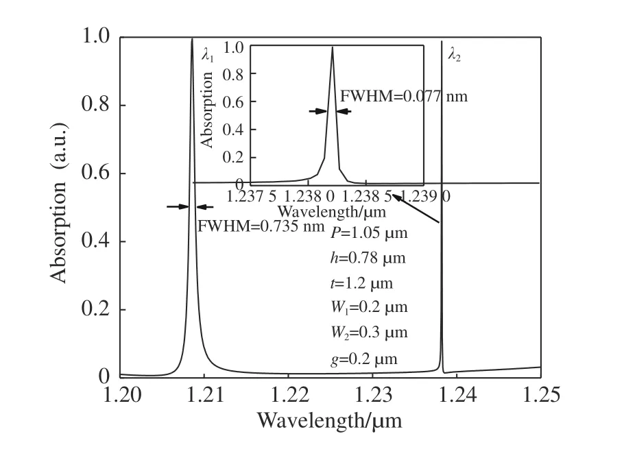
Fig.2 Absorption spectroscopy of dual-wavelength narrow-bandwidth dielectric MA图2 双波长窄带宽介质MA吸收光谱
MA can achieve ultra-narrow bandwidth high absorption at wavelengthsλ1=1.2085 μm andλ2=1.2382 μm because the effective impedance of MA at these two wavelengths just matches the free-space impedance and thus the reflection of MA at wavelengthsλ1andλ2can be effectively suppressed[23].Because the absorption efficiencyAof MA can be expressed asA=1-T-R, because the thickness of Au substrate is greater than the skinning depth of light, soT=0, and when the reflection of MA at wavelengthsλ1andλ2is suppressed, the absorption efficiency of MA at these two wavelengths can be close to 1.The effective impedanceZof MA can be expressed by Equation (2), whereS11andS21are the scattering matrix coefficients of reflection and transmission under vertical irradiation of TE polarized light, respectively, andR=(S11)2,T=(S21)2, and sinceT=0,S21=0.Figure 3 shows the effective impedance of MA calculated by Equation (2).
From Figure 3(a), it can be seen that the real part of impedanceZrealis close to 1 at wavelengthsλ1andλ2, while from Figure 3(b) it can be found that the imaginary part of impedanceZimagis close to 0 at wavelengthsλ1andλ2.


Fig.3 Effective impedance of dielectric MA.(a) Real part of impedance; (b) imaginary part of impedance图3 介质MA的有效阻抗。(a)阻抗实部;(b)阻抗虚部
In order to explore the intrinsic physical mechanisms of MA achieving dual-wavelength narrowbandwidth absorption, the electric field distribution of MA at wavelengthsλ1andλ2respectively, is calculated in this paper, as shown in Figure 4 (Color online).From Figure 4(a), it can be seen that the narrow-bandwidth dielectric MA has high narrowbandwidth absorption at wavelengthλ1because most of the light is confined in the SiO2dielectric layer, and a small portion of the light is confined in the asymmetric grating.It can be seen that the incident light forms a Fabry-Pérot (FP) cavity resonance in the SiO2dielectric layer.Figure 4(b) shows the electric field distribution of the narrow bandwidth dielectric MA at wavelengthλ2.Unlike the electric field distribution at wavelengthλ1, the light is no longer confined in the SiO2dielectric layer, but in the grating.Based on the electric field distribution,it can be judged that this is due to the formation of a guided mode resonance in the grating by the incident light[24], which also leads to a narrower bandwidth of the MA at wavelengthλ2.
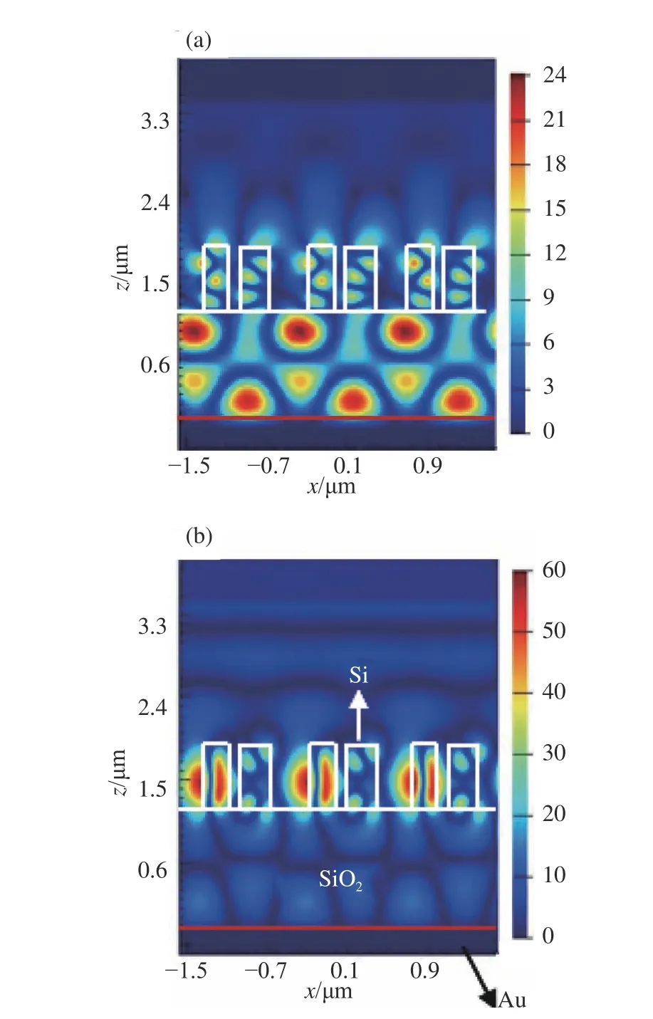
Fig.4 Electric field distribution of dual-wavelength narrow-bandwidth dielectric MA at different wavelengths.(a) λ1; (b) λ2图4 双波长窄带宽介质MA在不同波长处的电场分布。(a)λ1;(b)λ2
3.2 Effect of structural parameters on absorption characteristics of MA
In order to investigate the effect of MA structure parameters on the absorption characteristics of dual-wavelength narrow-bandwidth dielectric, the effect of MA structure parameters on its absorption characteristics is simulated and calculated in this paper.Figure 5 (Color online) shows the effect of different SiO2dielectric layer thicknesston MA absorption characteristics.From Figure 5(a), it can be seen that the absorption wavelengthλ1of MA is redshifted astincreases, however, the change inthas a very weak effect on the absorption wavelengthλ2.From Figure 5(b), it can be seen whentincreases from 1.2 μm to 1.215 μm, the absorption wavelengthλ1is red-shifted from 1.2085 μm to 1.2115 μm, an increase of 3 nm.The change inthas a significant effect on the MA absorption wavelengthλ1, which is due to the FP cavity resonance formed by the light in the SiO2dielectric layer as seen in Figure 4(a).The relationship between FP cavity resonance wavelength and SiO2layer thicknesstis shown in Equation (3)[25],

whereneqis the equivalent refractive index of FP cavity,Φis the sum of the phases of the upper and lower interfaces of the FP cavity, andNis an integer,λFPis the resonant wavelength of the FP cavity.According to Equation (3), it is known that an increase intincreases the FP cavity resonance wavelengthλFPwhich leads to a red shift in the absorption wavelengthλ1of MA.

Fig.5 Effect of t on the absorption characteristics of the dual-wavelength narrow-bandwidth dielectric MA.(a) Absorption spectra; (b) absorption wavelength图5 t对双波长窄带宽介质MA吸收特性的影响。(a)吸收光谱;(b)吸收波长
However, the reason why the increase inthas a weaker effect on the absorption wavelengthλ2of MA is that the narrow-bandwidth and high-absorption of MA at wavelengthλ2are caused by guided mode resonance, which can be seen from Figure 4(b).According to Ref.[26], the guided mode resonance wavelength is mainly related to the grating parameters and the incident angle.However, the absorption efficiency of MA at the absorption wavelengthλ2will gradually decrease astincreases,which can be explained by Figure 6 (Color online).Figure 6 is the electric field distribution of MA at wavelengthλ2whent=1.205 μm.Comparing Figure 6 with Figure 4(b), it can be found that the electric field focused in the grating in Figure 6 is significantly lower than Figure 4(b).Therefore, the absorption rate of MA will decrease aftertbecomes larger.
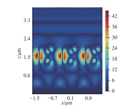
Fig.6 Electric field distribution of MA at wavelength λ2 when t = 1.205 μm图6 t=1.205 μm时MA在波长λ2处的电场分布
Figure 7 (Color online) shows the effect of grating widthW1on the absorption characteristics of dual-wavelength narrow-bandwidth dielectric MA.It can be seen from Figure 7(a) that the absorption wavelengthsλ1andλ2of MA both have red shifted asW1becomes larger, respectively.It can be seen from Figure 7(b) that whenW1increases from 0.2 μm to 0.202 μm, the absorption wavelengthλ2of MA is red-shifted by nearly 7 nm, while the absorption wavelengthλ1of MA is red-shifted by 1.46 nm.

Fig.7 Effect of W1 on the absorption characteristics of the dual-wavelength narrow-bandwidth dielectric MA.(a) Absorption spectra; (b) absorption wavelength图7 W1对双波长窄带宽介质MA吸收特性的影响。(a)吸收光谱;(b)吸收波长
The change ofW1can have an impact on the absorption wavelengthλ1because it can be known that the change of the grating width will lead to a change in the equivalent refractive index of the asymmetric grating, and the equivalent refractive index of the FP cavityneqis effectd by the equivalent refractive index of the asymmetric gratingnw.Moreover, it has been shown in Ref.[27] that the increase of the grating width will lead to the increase of the equivalent refractive index of the FP cavityneq.From Equation (3), it is known that an increase inneqwill increase the FP cavity resonance wavelengthλFP.And the increase ofλFPwill lead to the red-shift of the absorption wavelengthλ1of MA.Figure 8 showsneqvarying withW1and it is calculated by FDTD.From Figure 8, it can be found that whenW1increases from 0.2 μm to 0.202 μm,neqincreases from 1.510 to 1.512.

Fig.8 Effect of W1 on neq图8 W1对neq的影响
The grating, SiO2layer, and air form an optical waveguide, and according to the grating guidedmode resonance theory, it is known that the grating equivalent refractive index change will affect the guided-mode resonance wavelength[26], as shown in Equation (4).

whereλgis the guided-mode resonance wavelength andmis the diffraction order of the grating.According to the equivalent medium theory, an increase inW1will increase the grating equivalent refractive indexnw, and from Eq.(4), an increase innwwill redshift the guided-mode resonance wavelengthλgand thus the MA absorption wavelengthλ2will red-shift.The effect ofW2on MA absorption characteristics is not shown in this paper, because the effect of the change inW2on MA absorption characteristics is similar to that ofW1on MA, and the intrinsic physical mechanism of the effect is essentially the same.
The electric field distribution in Figure 4(b)shows that a part of the electric field is distributed among the slits of the dielectric grating, so it can be seen that the change of the surrounding gas will have an effect on the absorption wavelengthλ2of MA.Therefore, the narrow bandwidth dielectric MA proposed in this paper can be applied in the fields of gas or biological detection.In order to evaluate the performance of the narrow-bandwidth dielectric MA in gas detection, two parameters,sensitivity and quality factor, are defined, and the specific expressions are shown in equations (5) and(6).WhereSis the sensitivity of narrow-bandwidth MA,△nand△λare the amount of change in refractive index and the amount of change in absorption wavelength of the surrounding gas, respectively[18].
From Figure 9 (a) (Color online), it can be seen that the absorption wavelengthsλ1andλ2of MA are redshifted asnincreases.This is because a largernleads to a larger refractive indexnlof the grating's low refractive index material, which in turn leads to a larger equivalent refractive index of the grating for different wavelengths.And from the previous description, the grating refractive index will lead to a larger equivalent refractive indexneqof FP cavity,so according to Equation (3), the increase ofnwill lead to a red shift of MA absorption wavelengthλ1.Unlike the mechanism that causes the red shift of MA absorption wavelengthλ1,λ2is red-shifted asnbecomes larger, because the grating equivalent refractive indexnwincreases, which means that it increases the refractive index of the central layer of the optical waveguide, and this must lead to the red shift of the grating guided mode resonance wavelength according to the guided mode resonance theory and Equation (4)[27].

Fig.9 Effect of n on the absorption characteristics of the dual-wavelength narrow-bandwidth dielectric MA.(a) Absorption spectra; (b) absorption wavelength图9 n对双波长窄带宽介质MA吸收特性的影响。(a)吸收光谱;(b)吸收波长
From Figure 9(b), whennincreases from 1 to 1.03, the absorption wavelengthλ2increases from 1.2382 μm to 1.2417 μm, which is red-shifted by 3.5 nm, and according to Eqs.(5) and (6),S=117.3 nm/RIU and FOM = 1524/RIU.It can be found that the FOM in this paper is significantly improved compared to the references [14-15, 18].
Finally, the effect of the asymmetric grating periodPon the absorption characteristics of the dielectric MA was analyzed, and the specific results are shown in Figure 10 (Color online).From Figure 10, it can be found that the absorption wavelengthsλ1andλ2of MA are red-shifted with the increase ofP.WhenPincreases from 1.05 μm to 1.1 μm, the wavelengthλ1increases from 1.2085 μm to 1.2249 μm, while the wavelengthλ2increases from 1.2382 μm to 1.2525 μm.From Equation (4) we can know the reason why the wavelengthλ2increases with the increase ofP[24].When the period increases, if the guided mode resonance is to be maintained, the resonance wavelength must be shifted to the long wavelength direction.
AsPincreases, the phaseΦof the FP cavity decreases significantly because the effect of the change ofPonneqis not as significant as the phaseΦ.Therefore, according to Equation (3), it is known that the FP cavity resonance wavelengthλFPincreases with the increase ofP, which leads to the red-shift of the absorption wavelengthλ1of MA.The trend of the effect ofPon the phaseΦis calculated by FDTD and is shown in Figure 11, from which it can be seen thatΦdecreases from 4.64 rad to 0.22 rad whenPincreases from 1.05 μm to 1.1 μm.
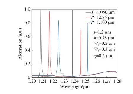
Fig.10 Effect of P on the absorption characteristics of the dual-wavelength narrow-bandwidth dielectric MA图10 P对双波长窄带宽介质MA吸收特性的影响

Fig.11 Effect of P on Φ图11 P对Φ的影响
4 Conclusion
In order to broaden the application field of narrow-bandwidth MA, a medium MA is designed in this paper that can achieve dual-wavelength narrowbandwidth absorption in the infrared band based on the finite-difference time-domain method.Through simulation analysis, the narrow bandwidth dielectric MA in this paper has ultra-high absorption efficiency at wavelengthλ1= 1.2085 μm andλ2= 1.238 2 μm, and the FWHM is only 0.735 nm and 0.077 nm, respectively.Because of the different mechanisms of MA forming narrow-bandwidth and high absorption onλ1andλ2, the study found thatλ1is very sensitive to the change of the thicknesstof the SiO2transition layer, whileλ2is very sensitive to the change of the dielectric grating widthW1.With the increase oftandW1, the absorption wavelengthsλ1andλ2of MA will red-shift respectively.When the grating periodPincreases, the absorption wavelengthsλ1andλ2of MA will shift to the long wavelength direction at the same time.From the electric field distribution of MA atλ2, a large part of its electric field is distributed in the gap between the gratings, so the change of air refractive index has a significant effect onλ2.This allows it to be used in the field of detection.It is calculated that the FOM of the narrow-bandwidth dielectric MA in this paper can reach 1524/RIU.
——中文对照版——
1 引言
在许多应用中都有需要对电磁波实现完美吸收,如太阳能电池、热发射器、辐射冷却、通信等[1-4]。但是由自然界存在的材料构成的吸收器因缺乏磁响应导致阻抗失配,因此它们不能完全抑制光反射,从而降低了吸收器光吸收能力[5]。因此,人们提出了基于超材料的吸收器,由于超材料吸收器(Metamaterial Absorber,MA)对电磁波具有高吸收效率,且具有体积小、可设定工作波长等优点,逐渐被人们所关注并成为研究热点之一[6]。
经深入研究,人们设计并制备出了不同类型的MA,如宽带宽MA、窄带宽MA、太赫兹MA、可调谐MA等[7-9]。窄带宽MA被人们所关注是因为窄带宽MA用在探测和热发射器上时相比于宽带宽MA效率更高[10-11],而且在光调制、光探测和热辐射剪裁中只有窄带宽MA才能满足要求[12-13]。目前已经有不同结构的窄带宽MA被提出,如基于裂环谐振器阵列(Split Ring Resonator,SRR)、金属/介质周期光栅、金属/介质狭缝(narrow slits)等。2014年瑞典皇家理工学院的Min-Qiu等人提出在银(Ag)金属衬底上刻蚀金属光栅,基于Ag光栅与空气介质形成的表面等离子激元共振成功使MA在波长1400 nm处实现了窄带宽吸收,其线宽(Full Width Half Maximum,FWHM)可以达到0.4 nm[14];2018年香港中文大学的FENG A等人提出一种由非对称金属光栅和金属衬底构成的窄带宽MA,而且在光栅和衬底之间添加了一层二氧化硅过渡层,经模拟计算发现该窄带宽MA在光通信波段实现了超窄吸收,FWHM仅 有0.28 nm[15];2019年,东 南 大学KANG S等人提出在二氧化硅衬底上刻蚀出由金(Au)材料构成的十字型纳米阵列,与此同时在二氧化硅另一面生长一层Au薄层抑制透射,经测试发现该MA可在太赫兹波段实现窄带宽吸收[16]。
从以上研究可以发现,这些窄带宽MA中的微纳结构所使用的材料都是金属材料,但是金属材料存在欧姆损耗,而且在高频处精细金属材料存在加工问题,这会在一定程度上影响MA在将来的应用推广。因此,一些课题组提出利用介质材料设计、制造窄带宽MA。2019年哈尔滨工业大学的Zhibin Ren等人利用氮化硅、氧化铟锡材料设计并制备出在红外波段具有窄带宽吸收的MA,经测试可得该窄带宽MA的FWHM可达2.6 nm[17];2020年,安徽大学的Yan Zhao等人提出在金属衬底上直接刻蚀出由硅材料构成的介质光栅,经模拟计算可知该窄带宽MA的FWHM可达0.38 nm[18]。
虽然利用介质材料设计制备窄带宽MA可以降低制造成本,提高吸收效率,而且吸收带宽可保持在亚纳米级别,但目前鲜有实现多波长窄带宽亚纳米级别吸收的MA,这会限制窄带宽MA在一些场合的应用,如在光谱探测、气体探测中,多波长窄带宽MA更能提高它们的工作效率[19-20]。针对上述需求,本文提出由非对称介质光栅、介质过渡层、金属衬底构成的双波长窄带宽介质MA,并利用时域有限差分法(Finite Difference Time Domain, FDTD)对该MA进行设计和分析。FDTD在时域中对麦克斯韦方程组的微分形式进行数值求解,以差商代替方程中的微分。在求解时电场与磁场交替分布,随着时间的推移求解出仿真区域的电场和磁场。经模拟计算发现双波长窄带宽MA的FWHM最低可达0.077 nm,品质因素(Figure Of Merit,FOM)可达1524/RIU,而且经对比可以发现本文设计的窄带宽MA最窄的吸收带宽相比文献[14-18]都下降了一个数量级。本文研究可为生物传感器、热发射器、光调制器等提供高质量的双波长窄带宽介质MA。
2 器件结构
图1是双波长窄带宽介质MA结构图,它自下而上由Au衬底、二氧化硅(SiO2)介质层、硅(Si)材料形成的非对称光栅组成。Au衬底的主要作用是抑制光的透射,因此它的厚度必须大于入射电磁波的趋肤深度,本实验中Au的厚度设为0.2 μm。从图1中可以看到,一个周期内具有两个同高度(h)、不同宽度的光栅,它们的宽度分别是W1和W2,同周期内光栅之间的间距为g,另外SiO2的厚度为t。在将来实际器件制备中,本文的双波长窄带宽介质MA的制备工艺与现今的微纳加工工艺兼容,通过磁控溅射在Au衬底上先后生长SiO2和Si薄层,紧接着在Si薄层上旋涂电子束抗蚀胶,经电子束曝光和显影后在抗蚀胶上形成非对称光栅图形,去胶并利用感应耦合等离子体刻蚀技术,将图形转移到Si薄层上,最终制备出双波长窄带宽介质MA[21]。
Au的介质常数由Drude模型表示,即

式中ωp、γ和ω分别是等离子体频率、阻尼系数和入射光角频率。为了保证模拟计算结果正确,ωp和γ均是从实验数据中获得,根据文献[22]可知,ωp=1.32×10¹⁶rad/s,γ=1.2×1014rad/s。SiO2和Si的折射率分别为nSiO2=1.45和nSi=3.45。
3 结果与讨论
3.1 双波长窄带宽高吸收的实现
首先利用FDTD软件建立双波长窄带宽介质MA单个周期的二维物理模型,然后在x方向添加周期性边界条件,在z方向添加完美匹配层边界条件,y方向默认为光栅无限长。最后在双波长窄带宽介质MA正上方添加光源,光源偏振设为TE偏振,入射角设为0°,并且MA周围为空气,折射率n=1。
图2所示的是双波长窄带宽介质MA的吸收光谱,此时P=1.05 μm、t=1.2 μm、h=0.78 μm、W1=0.2 μm、W2=0.3 μm、g=0.2 μm,上述光栅参数是基于FDTD优化后获得的。从图2中可以看到MA分别在波长λ1=1.2085 μm和λ2=1.2382 μm处具有超高吸收效率,吸收线宽FWHM分别为0.735 nm和0.077 nm。相比于文献[14-15, 17]结果,双波长窄带宽介质MA在波长λ2处的线宽明显下降,实现了窄带宽吸收。若无特殊说明,上述所有参数保持不变。
MA能在波长λ1=1.2085 μm和λ2=1.2382 μm实现超窄带宽高吸收,是因为MA在这两个波长处的有效阻抗刚好与自由空间阻抗相匹配,这可有效地抑制MA对波长λ1和λ2的反射[23]。因为MA的吸收效率A可表示为A=1-T-R,由于Au衬底的厚度大于光的趋肤深度,所以T=0,而当MA在波长λ1和λ2的反射得到抑制后,MA对这两个波长的吸收效率就接近1。MA的有效阻抗Z可由式(2)表示:

式中S11和S21分别是TE偏振光垂直照射下反射和透射的散射矩阵系数,其中R=(S11)2,T=(S21)2,由于T=0,所以S21=0。图3是由式(2)计算得到的MA的有效阻抗,从图3(a)中可知阻抗的实部Zreal在波长λ1和λ2处接近为1,而从图3(b)中可以发现阻抗的虚部Zimag在波长λ1和λ2接近为0。
为了探索MA实现双波长窄带宽吸收的内在物理机制,本文计算了MA分别在波长λ1和λ2处的电场分布,具体如图4(彩图见期刊电子版)所示。从图4(a)中可知,窄带宽介质MA之所以在波长λ1出现窄带宽高吸收是因为大部分光被限制在SiO2介质层当中,少部分光限制在非对称光栅当中。由此可知,入射光在SiO2介质层当中形成了法布里-珀罗(Fabry-Pérot, FP)腔共振。图4(b)所示的是窄带宽介质MA在波长λ2的电场分布,与在波长λ1的电场分布不同,此时光不再被限制在SiO2介质层当中,反而是被限制在光栅当中,依据电场分布可以判断这是由于入射光在光栅中形成了导模共振[24],也因为导模共振导致MA在波长λ2处的带宽更窄。
3.2 结构参数对MA吸收特性的影响
为了探究双波长窄带宽介质MA结构参数对其吸收特性的影响规律,本文模拟计算了MA结构参数对其吸收特性的影响。图5(彩图见期刊电子版)是不同SiO2介质层厚度t对MA吸收特性的影响。从图5(a)中可知,随着t的增加,MA的吸收波长λ1会出现红移现象,但是t的变化对吸收波长λ2的影响非常微弱。由图5(b)可得,当t从1.2 μm增加到1.215 μm,吸收波长λ1从1.2085 μm红移到1.2115 μm,增加了3 nm。t的变化能够对MA吸收波长λ1有显著影响,是因为由图4(a)可知光在SiO2介质层中形成了FP腔共振。FP腔共振波长与SiO2层厚度t的关系为[25]:

式中,neq是FP腔的等效折射率,Φ是FP腔上下界面相位之和,N是整数,λFP是FP腔共振波长。根据式(3)可知t增大会导致FP腔共振波长λFP增大,从而导致MA的吸收波长λ1出现红移现象。
由图4(b)可知,MA在波长λ2处实现窄带宽高吸收是因为导模共振效应,而根据文献[26]可知,导模共振波长主要与光栅参数、入射角等有关。但是可以发现随着t的增大,MA在吸收波长λ2的吸收效率会逐渐下降,这可由图6(彩图见期刊电子版)解释。图6是t=1.205 μm时MA在波长λ2处电场分布,将图6与图4(b)相比,可以发现在图6中聚集在光栅中的电场明显低于图4(b),故此导致MA在t变大后的吸收率会下降。
图7(彩图见期刊电子版)所示的是光栅宽度W1对双波长窄带宽介质MA吸收特性的影响。由图7(a)可知,随着W1的变宽,MA的吸收波长λ1和λ2都分别出现了红移现象。从图7(b)可知,当W1从0.2 μm增加到0.202 μm,MA的吸收波长λ2红移了将近7 nm,而MA的吸收波长λ1红移了1.46 nm。
W1的变化能够对吸收波长λ1产生影响是因为根据等效介质原理可知光栅宽度的变化会导致非对称光栅的等效折射率发生变化,而FP腔的等效折射率neq又受非对称光栅等效折射率nw的影响。而且文献[27]也已经证明,光栅宽度增加会导致FP腔等效折射率neq增大,由式(3)可知,neq增大,FP腔共振波长λFP也将会增大。λFP增大就会导致MA的吸收波长λ1红移。图8是当W1取不同值时neq的变化情况,它是由FDTD计算获得。从图8中可以发现,当W1从0.2 μm增加到0.202 μm,neq则从1.510增加到1.512.
光栅、SiO2层、空气形成了光波导,根据光栅导模共振理论可知,光栅等效折射率的改变将会影响导模共振波长[26],即

式中λg是导模共振波长,m为光栅的衍射阶数。由等效介质理论可知,W1增大将会使光栅等效折射率nw增大,而根据式(4)可知,nw增大则使导模共振波长λg红移,从而使MA吸收波长λ2红移。在本文中之所以没有展示W2对MA吸收特性的影响,是因为W2的变化对MA吸收特性的影响与W1对MA的影响相似,而且内在物理机理也基本相同。
通过图4(b)的电场分布可知,有一部分电场分布在介质光栅缝隙中,由此可知,周围气体的变化将会对MA的吸收波长λ2产生影响,因此本文提出的窄带宽介质MA可应用在气体或生物探测等领域当中。为了评估窄带宽介质MA在气体探测中的工作性能,定义了灵敏度和品质因素两个参数,即

式中S是窄带宽MA的灵敏度,△n和△λ分别是周围气体折射率的变化量和吸收波长的变化量[18]。
从图9(a)(彩图见期刊电子版)可知,随着n的增加,MA的吸收波长λ1和λ2都出现了红移的现象。因为n变大会导致光栅低折射率材料折射率nl变大,而nl变大又会导致光栅对不同波长的等效折射率变大。而由前面所述可知,光栅折射率变大会导致FP腔等效折射率neq变大,所以根据式(3)可知,n的增加会导致MA吸收波长λ1红移。与导致MA吸收波长λ1红移的机理不同,MA吸收波长λ2之所以会随着n变大而红移,是因为其增大了光栅等效折射率nw,这意味着增大了光波导中心层的折射率,而根据导模共振理论和式(4)可知[27],这必定会导致光栅导模共振波长的红移。
从图9(b)可知,当n从1增加到1.03,吸收波长λ2会从1.2382 μm增加到1.2417 μm,红移了3.5 nm,根据式(5)和式(6)可得,S=117.3 nm/RIU,FOM=1524/RIU。本文的FOM相比文献[14-15, 18]有了明显提高。
最后分析了非对称光栅周期P对介质MA吸收特性的影响,具体结果如图10(彩图见期刊电子版)所示。从图10中可以发现,随着P的增加,MA的吸收波长λ1和λ2都产生了红移现象。当P从1.05 μm增加到1.1 μm后,波长λ1则从1.2085 μm增加到了1.2249 μm,而波长λ2则从1.2382 μm增加到了1.2525 μm。由式(4)可知,波长λ2之所以会随着P的增大而增大[24],是因为周期增大时若要维持导模共振,则必须使得共振波长向长波长方向移动。
随着P的增加FP腔的相位Φ会显著下降,因为P的变化对neq的影响并无相位Φ的显著,所以根据式(3)可知,随着P的增加FP腔共振波长λFP会增大,从而导致MA的吸收波长λ1出现红移现象。P对相位Φ的影响趋势如图11所示,该结果由FDTD计算得到,从图11中可知当P从1.05 μm增大到1.1 μm,Φ会从4.64 rad下降到0.22 rad。
4 结论
为了拓宽窄带宽MA的应用领域,本文基于时域有限差分法设计了在红外波段上可实现双波长窄带宽吸收的介质MA,经模拟分析发现,本文的窄带宽介质MA在波长λ1=1.2085 μm和λ2=1.2382 μm具有超高吸收效率,而且FWHM也分别只有0.735 nm和0.077 nm。由于MA在λ1和λ2上形成窄带宽高吸收的机理不同,所以经本文研究发现,λ1对SiO2过渡层的厚度t变化非常敏感,但是λ2却对介质光栅宽度W1的变化非常敏感,随着t和W1的增加,MA的吸收波长λ1和λ2都会分别出现红移现象。而当光栅周期P增加时,MA的吸收波长λ1和λ2会同时向长波长方向偏移。从MA在λ2处的电场分布可知,其电场有一大部分是分布在光栅之间的空隙当中,因此空气折射率的变化对λ2有显著影响,这可使其应用在探测领域当中,经计算可得本文的窄带宽介质MA的FOM可达1524/RIU。
猜你喜欢
中国交通信息化(2021年1期)2021-06-11
数学年刊A辑(中文版)(2018年2期)2019-01-08
中国科技信息(2016年6期)2016-08-31
数学理论与应用(2016年4期)2016-05-17
山西大同大学学报(自然科学版)(2016年6期)2016-01-30
中国科技信息(2015年24期)2015-11-07
中国科技信息(2015年23期)2015-11-07
电测与仪表(2015年4期)2015-04-12
物理实验(2015年9期)2015-02-28
中国眼镜科技杂志(2014年8期)2014-09-08