
Hybrid-anode structure designed for a high-performance quasi-vertical GaN Schottky barrier diode
2022-05-16 07:12QiliangWang王启亮TingtingWang王婷婷TaofeiPu蒲涛飞ShaohengCheng成绍恒XiaoboLi李小波LiuanLi李柳暗andJinpingAo敖金平
Chinese Physics B 2022年5期
关键词:金平
Qiliang Wang(王启亮) Tingting Wang(王婷婷) Taofei Pu(蒲涛飞) Shaoheng Cheng(成绍恒)Xiaobo Li(李小波) Liuan Li(李柳暗) and Jinping Ao(敖金平)
1State Key Laboratory of Superhard Materials,Jilin University,Changchun 130012,China
2Shenzhen Research Institute,Jilin University,Shenzhen 518057,China
3National Key Discipline Laboratory of Wide Band-gap Semiconductor,School of Microelectronics,Xidian University,Xi’an 710071,China
4Institute of Technology and Science,Tokushima University,Tokushima 770-8506,Japan
Keywords: Schottky barrier diode,hybrid anode,dielectric,edge termination
1. Introduction
The GaN-based vertical power devices have emerged as the promising candidates for next-generation high-efficiency power electronics because they can realize higher breakdown voltage in small areas,free of surface traps,and good thermal properties.[1–3]Among the GaN-based power devices, Schottky barrier diodes (SBDs) possess the advantages of low forward turn-on voltage (Von) and no minority carrier storage,which are beneficial to realize low conduction/switching loss and fast-switching speed.[4,5]Although high-performance vertical GaN-on-GaN SBDs have been investigated extensively along with the development of the freestanding GaN substrate,the commercial GaN substrate is still limited by the high cost and the small diameter.[6]
On the other hand, GaN epitaxy on low-cost and largearea foreign substrates (silicon, sapphire, etc.) provides the feasibility of quasi-vertical GaN SBDs.[7,8]However, the breakdown voltage of the quasi-vertical SBDs at reverse bias is far below the GaN material limit.The premature breakdown is ascribed to some critical issues such as high dislocation density, high background doping concentration of the drift layer,leakage current from the etched mesa sidewall,and the termination techniques. The former issues can be effectively solved by improving the crystalline quality of GaN epitaxy material and optimizing the device fabrication process.In addition,different kinds of termination technologies are developed to improve the breakdown voltage in recent years.[9,10]
Generally,the junction barrier Schottky structure by partially replacing the drift layer with p+region is the most effective route based on the charge-coupling. The reversely biased p–n junction results in a lateral depletion of the drift layer,which can effectively shield the strong electric field at the Schottky contact. However, the p+region obtained by epitaxy growth or ion-implantation encounters significant technical challenge during the thermally activation.[11–13]Some alternative methods such as nitrogen or the fluorine plasma treatment, field plate (FP) structure, and trench metal-oxidesemiconductor (MOS) barrier-controlled Schottky have been developed.[14–16]The introduction of dielectric layer is effective to reduce the peak electrical field with a simple fabrication process.
In this work,we proposed a hybrid anode structure to realize the high-performance quasi-vertical GaN Schottky barrier diode. The SiN dielectric is not only used at the mesa edge, but also adopted in the main Schottky contact area. By optimizing the thickness and length of SiN,a balance between on-resistance and breakdown voltage is obtained. In addition,the SiN dielectric on the side wall is also covered by the anode metal as a FP structure. The effect of SiN dielectric on the performance of the diode has been evaluated extensively through Silvaco technology computer-aided design (TCAD)2-D device simulation.
2. Experiment
The SBDs structures used for simulation are shown in Fig. 1. The epi-wafer comprises a 2 μm n+-GaN layer (impurity density over 1×1018cm-3)and a 6 μm n--GaN drift layer (impurity density of 1×1016cm-3) on sapphire. The dimensions of the ohmic cathode contact, the cathode–anode distance,and the mesa width are 2 μm,10 μm,and 20 μm,respectively. For the reference diode,the anode metal is 18 μm without the SiN dielectric. While for the hybrid anode structure, the SiN dielectric (thickness of 20 nm) covers all the mesa area and patterned on the surface with different lengths(L=0.5 μm, 2 μm, and 4 μm, respectively). Furthermore,to fabricate the FP,the anode metal(Ni in our experiment)is expanded into 21 μm with 0.5 μm overlap at the two edges of mesa. The device width along thez-axis(perpendicular to the paper)is defaulted as 1 μm. The current–voltage(I–V)curves of the SBDs were obtained by the TCAD simulation, including the parallel-electric-field-dependent mobility model, the Auger recombination model,and the impact ionization model.A universal phonon-assisted tunneling model is also defined at the anode region.[17]
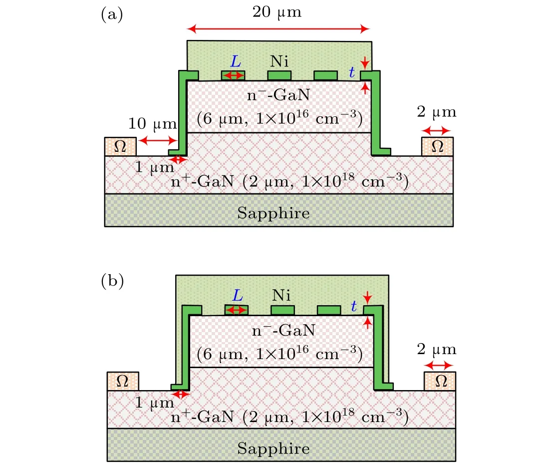
Fig. 1. The schematic structure of the hybrid anode SBDs without (a) and with(b)a side-wall field plate.
3. Results and discussion
Firstly,we evaluated the effect of the SiN dielectric layer on the electrical behaviors of the SBDs. The thickness and length of the SiN were set to 20 nm and 0.5 μm,respectively.The obtainedI–Vcurves were plotted in the linear and the semi-logarithm coordination as shown in Figs. 2(a) and 2(b),respectively. It demonstrates that theI–Vcurves at the forward bias region are nearly the same for two SBDs,implying the hybrid anode shows a weak effect on the current conduction path. The current density distribution of the reference and the hybrid-anode SBDs under 0.5 V,1.0 V,and 2.0 V bias were simulated by TCAD(Fig.3). It clearly shows that the current density is relatively smaller beneath the dielectric layer,[18]but this effect is very weak especially at a relatively high forward bias.
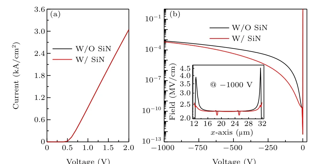
Fig.2. The forward I–V characteristics in linear(a)and semi-logarithm(b)coordinate of the reference and hybrid anode diode. The inset of (b) is the electric field obtained along cutline AA′ under-1000 V.
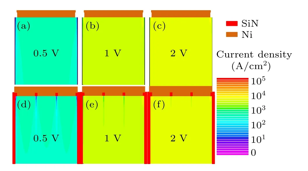
Fig. 3. The current density distribution at 0.5 V, 1 V, and 2 V forward bias for the diode without(a)–(c)and with SiN dielectric pattern(d)–(f).
On the other hand,the introduction of the SiN decreases the reverse leakage current effectively(approximately 2 orders of magnitude)(Fig.2(b)). The electric field distribution under-1000 V shows an obvious electric field crowding effect at the edge of anode for the diode without SiN (Fig. 4), presenting a maximum electric field of approximately 4.5 MV/cm (inset of Fig. 2(b)). This value is much higher than the critical electric field of GaN, implying the breakdown voltage of the reference SBD is smaller than 1000 V.For the diode with a patterned SiN dielectric,the electric field crowding is effectively suppressed with the maximum electric field of approximately 2.5 MV/cm. It is worth noting that the minimum electric field occurs beneath the SiN dielectric. The charge-coupling effect between the insulation layer dielectric and GaN generates a 2-D depletion in the drift layer,which could correspondingly reduce the electric field magnitude and enhance the breakdown voltage.[15]In addition, it can be found that the increase of SiN thickness could weaken this charge-coupling effect (not shown), which is consistent with previous reports.[15]Based on those results,the thickness of the SiN is set to 20 nm in the following investigations.
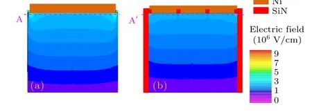
Fig.4. The electric field distribution of the reference diode(a)and the hybrid anode diode(b)under-1000 V.The electric field of both diodes are obtained along the cutline AA′ for comparison.
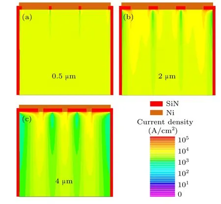
Fig.6. The current density distribution under 2 V forward bias for the diode with 0.5 μm(a),2 μm(b),and 4 μm(c)SiN dielectric layer.

Fig. 7. The electric field distribution of the reference (a) and hybrid anode(b)diode under-1000 V.
Another key parameter of the SiN is the length under the Schottky anode on the top surface. Herein,we evaluated three lengths of 0.5 μm,2 μm,and 4 μm when kept a thickness of 20 nm of SiN.The simulatedI–Vcharacteristics were plotted in the linear and the logarithm coordinate,showing good rectification characteristics for all the diodes(Fig.5). The current density at the forward bias region decreases obviously with the increasing SiN length, while the turn-on voltages are nearly the same(Fig.5(a)). The possible reason may be ascribed to the increasing series resistance as discussed in our previous work.[5,18]Based on the thermionic emission(TE)model,the series resistances are deduced as shown in inset of Fig. 5(b).To reveal the mechanism more detailly,the current density distribution at 2.0 V bias were simulated by TCAD to evaluate the SiN length on the current density of hybrid-anode SBDs(Fig.6). It clearly shows that the current density is relatively small beneath the dielectric layer. However,this effect is very weak when the dielectric layer is relatively short but became strong when the length is long especially for the 4 μm sample.At the reverse bias region,a longer SiN helps to suppress the leakage slightly until-1000 V(Fig.5(b)). This phenomenon can be attributed to the expending low electric field regions beneath the SiN with the increasing length. In addition, the electric field beneath the SiN is obviously smaller than that of Ni/Au metal contact(Fig.7).
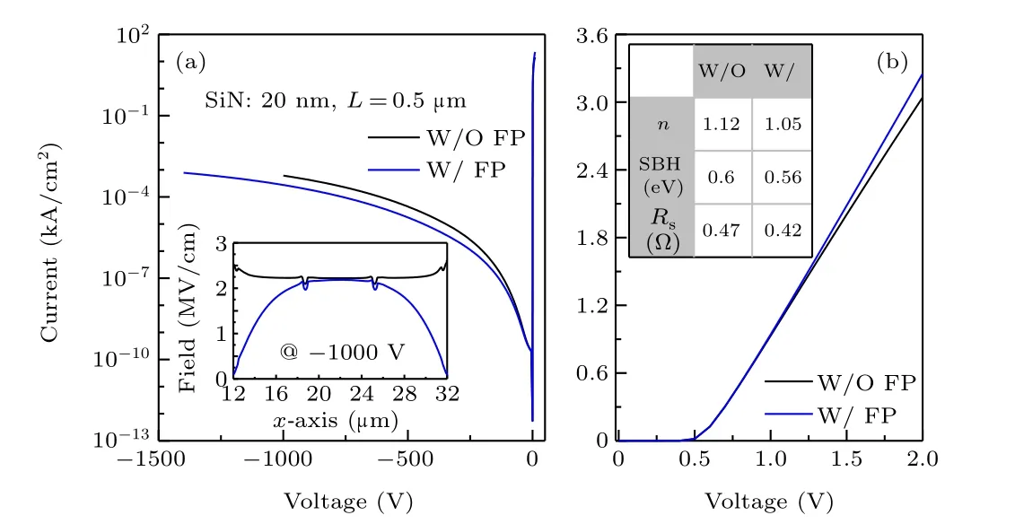
Fig.8. The forward I–V characteristics in semi-logarithm(a)and linear(b)coordinate of the hybrid anode diode with and without the FP. Inset of (a)is the electric field distribution under -1000 V and the inset of (b) is the corresponding parameters by fitting the curves with the TE model.
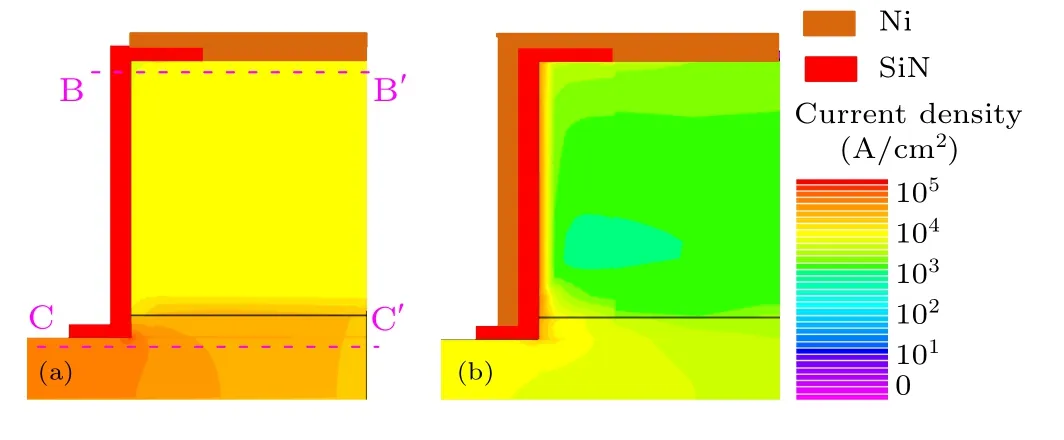
Fig.9. The current density distribution under 10 V forward bias for the diode without(a)and with(b)a sidewall field plate structure.
Figure 8 shows the effect of the field plate on the electrical behaviors of the SBDs. It demonstrates that theI–Vcurves of the SBDs without and with a field plate present comparable rectification characteristics excepting slight discrepancy. At the reverse bias region, the FP structure(20 nm SiN,LFP=0.5 μm)helps to suppress the leakage slightly until-1000 V (Fig. 8(a)). On the other hand, the two curves are nearly the same at the forward bias below 1.5 V,while the current density increases slightly at higher forward bias for the diode with the field plate(Fig.8(b)). By fitting the curves with TE model,the key parameters shown in inset of Fig.8(b)are comparable for both diodes. However,the introduction of the FP decreases the series resistance. The current density distribution for the two kinds of SBDs at a relatively higher forward bias(10 V)is also shown in Fig.9. Obviously,the diode with the FP structure forms a MOS channel along the side wall with a higher current density,while the current density in the central drift layer is suppressed. This phenomenon is also confirmed from Fig. 10 (obtained along cutline BB′and CC′). This appearance of the sidewall channel leads to a smaller resistance,especially when the forward bias is relatively larger.
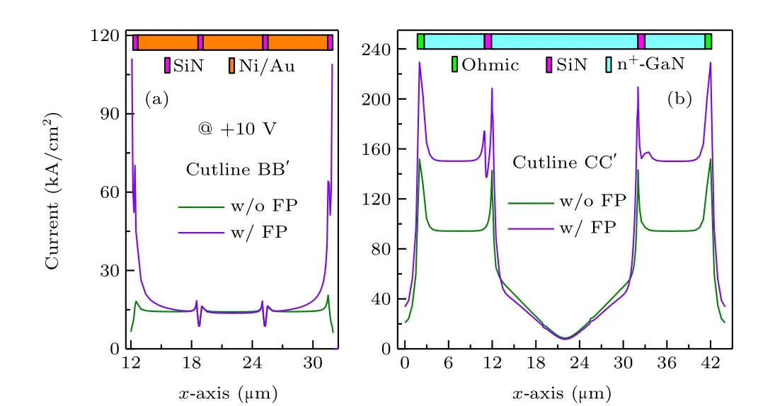
Fig. 10. The current density distribution around the top (a) and bottom (b)region of the mesa at 10 V forward bias for the diode without and with a sidewall field plate structure.
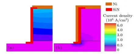
Fig.11. The electric field distribution under a reverse voltage of-1000 V of the diode without(a)and with(b)a sidewall field plate structure.
To understand the mechanism of those results,the distribution of the electric field was simulated by TCAD as shown in Fig. 11. At-1000 V, the electric field distribution in the diode without the FP is relatively even with slight crowding effect at the edge of mesa. In addition, the electric field beneath the SiN is obvious smaller than that of Ni/Au metal contact. This result can also be confirmed from inset of Fig.8(a)(obtained along cutline BB′),in which the maximum and minimum electric field are approximately 2.5 MV/cm and 2.0 MV/cm around the edge and the dielectric, respectively.For comparison,the FP structure can suppress the electric field effectively especially at the sidewall. However, the electric field distribution shows an obvious crowding effect at the bottom of mesa for the diode with the FP structure(Fig.4). In the vertical diode, it was reported that a deep mesa is beneficial to suppress the electric field.[16]The possible reasons for this discrepancy may be ascribed as follows. On the one hand,the conduction path and the electric field will generate a sharp turn at the bottom of the mesa due to the quasi-vertical structure.On the other hand, a vertical mesa is adopted in our simulation with an angle of 90°. A beveled mesa with a relatively small angle is required for the further optimization.[19]Owing to the lack of native dielectric for GaN-base materials. The introduction of the dielectric needs to cope with the inferior film bulk and interface quality,especially as many etching damages exist on the side wall during the mesa fabrication. The highquality LPCVD-SiN with a remote plasma treatment presents an obvious enhanced reliability,[20]which is promising for the device proposed in this work.
4. Conclusion and perspectives
In conclusion,a hybrid anode structure is proposed to improve the electrical properties of the quasi-vertical GaN Schottky barrier diode.For the conventional diode without a SiN dielectric layer,an obvious electric field crowding occurs at the edge of anode and decreases the breakdown voltage. The introduction of a small length SiN dielectric is beneficial to suppress the electric field crowding to enhance breakdown voltage. In addition, the forward current density is comparable although the dielectric layer diminishes the conduction path slightly. However, the conduction path decreases drastically for the diode with an increasing SiN dielectric length, resulting in a high on-resistance. Finally,the introduction of a field plate on the side wall forms a MOS channel and decreases the series resistance, but also shows an obvious electric field crowding effect at the bottom of the mesa. A beveled mesa with a relatively small angle is required for further optimization.
Acknowledgment
Project supported by the Key-Area Research and Development Program of Guangdong Province, China (Grant No. 2020B0101690001) and the Natural Science Foundation of Sichuan Province,China(Grant No.22YYJC0596).
猜你喜欢
Chinese Physics B(2022年10期)2022-10-26
Plasma Science and Technology(2022年8期)2022-09-14
意林彩版(2022年1期)2022-05-03
Chinese Physics B(2022年4期)2022-04-12
船电技术(2022年3期)2022-03-19
诗潮(2021年11期)2021-11-24
红河学院学报(2021年4期)2021-11-19
新农村(2017年20期)2017-09-28
今古传奇·故事版(2016年23期)2017-01-12
故事会(2016年21期)2016-11-10

- Chinese Physics B的其它文章
- A nonlocal Boussinesq equation: Multiple-soliton solutions and symmetry analysis
- Correlation and trust mechanism-based rumor propagation model in complex social networks
- Gauss quadrature based finite temperature Lanczos method
- Experimental realization of quantum controlled teleportation of arbitrary two-qubit state via a five-qubit entangled state
- Self-error-rejecting multipartite entanglement purification for electron systems assisted by quantum-dot spins in optical microcavities
- Pseudospin symmetric solutions of the Dirac equation with the modified Rosen–Morse potential using Nikiforov–Uvarov method and supersymmetric quantum mechanics approach