
Modulation of Schottky barrier in XSi2N4/graphene(X =Mo and W)heterojunctions by biaxial strain
2022-08-31 09:58QianLiang梁前XiangYanLuo罗祥燕YiXinWang王熠欣YongChaoLiang梁永超andQuanXie谢泉
Chinese Physics B 2022年8期
Qian Liang(梁前), Xiang-Yan Luo(罗祥燕), Yi-Xin Wang(王熠欣),Yong-Chao Liang(梁永超), and Quan Xie(谢泉)
College of Big Data and Information Engineering,Institute of New Optoelectronic Materials and Technology,Guizhou University,Guiyang 550025,China
Keywords: MoSi2N4,Schottky barrier height,heterojunction,biaxial strain
1. Introduction
Since the first exfoliation of graphene from graphite,[1]graphene — a two-dimensional (2D) allotrope of carbon —has ignited more and more interest from researchers because of its excellent mechanical properties[2]and ultra-high carrier mobility(∼2.5×104cm2/V·s in room temperature).[3]Soon after, a growing body of 2D materials, such as silylene,[4]hexagonal boron nitride(h-BN),[5]black phosphorus(BP),[6,7]and transition metal dichalcogenides (TMDCs),[8]have received much attention. Notably, MoS2,[9]WS2,[10]and WSe2[11,12]are all in a family of TMDCs, whose extraordinary potentials in electronic,[13,14]optoelectrical,[15]and valleytronic[16]applications have been studied. However, the zero band gap of graphene is the biggest problem,which limits its applications in electronic devices. Meanwhile, vdW heterojunctions composed of vertically stacked 2D materials have been put forward and have provided wide possibilities in band structure engineering projects. Especially, graphene can build weak interlayer coupling with other 2D materials because of unique properties of lacking dangling bonds.Symmetry breaking of graphene leads to an intrinsic built-in electric field,bringing many more unparalleled nanoelectronic and optoelectronic properties to graphene-based heterojunctions far beyond those of monolayers. Graphene-based vdW heterojunctions were studied not only in theory, but also in experiment all over the world. For example,Siet al.[17]studied the electronic structure and interface properties of the vdW heterostructure composed of single layers of GaSe and graphene,leading the Schottky barrier heights (SBHs) to be controlled by applying an external electric field. A MoS2/graphene heterojunction was successfully synthesized by Huanget al.,[18]and it exhibited excellent broad light absorption as well as high charge separation,hoping to be used as electrodes to fabricate photoelectrochemical-type photodetectors. In addition, Royet al.[19]demonstrated that graphene–MoS2hybrids can be used as high-sensitive gate-tunable photodetectors and optical switches.
Very recently, a newly graphene-like 2D material —MoSi2N4(MSN) — was synthesized by using chemical vapor deposition (CVD) method by Honget al.[20]TheMA2Z4family were also predicted to be dynamically stable in the air,whereMdenotes a transition metal (Mo, W, V, Nb, Ta, Ti,Zr, Hf, or Cr),Ais Si or Ge, andZrepresents N, P, or As.MA2Z4family exhibit exceptional piezoelectricity, high thermal conductivity, stiffness and promising photocatalysis.[21]Wuet al.[22]found that by applying biaxial strain and external electric field, band gaps of MSN and WSi2N4(WSN)can be tuned by both compress and tensile strain. Compress strain can even lead to the transition fom indirect bandgap to direct bandgap and external electric field can also give rise to the transition from semiconductor to metal. Jianet al.[23]reported that tensile MSN possesses the best optical absorption efficiency ever shown in the visible region, which has great potential applications in optoelectronic devices. In addition,Zanget al.[24]and Qianet al.[25]demonstrated that when introducing surface nitrogen vacancy, MSN, and WSN exhibit the highly desirable hydrogen evolution reaction (HER) catalytic activities, which highlights a family of potential HER electrocatalysts.
Generally,the electronic properties of graphene and other 2D materials are very sensitive to the external conditions,such as the induction of doping elements, external electric field, external strain and substrate interactions. In this work,given that the modulation of the SBHs of heterojunctions composed of graphene and MSN or WSN by biaxial strain has not been investigated yet, we construct MSN/graphene and WSN/graphene two heterojunctions. Firstly, we calculate the binding energy to ensure the stability of the heterojunctions.Then we study the electronic properties of two heterojunctions, including band structures and density of states (DOS).We also further investigate charge transfer between monolayer MSN or WSN and monolayer graphene. Finally,we modulate the SBHs of heterojunctions by applying external strain, realizing dynamic switching either between n-type and p-type Schottky contacts, or between Schottky contacts and Ohmic contacts.
2. Computational method
The structural optimization and electronic properties of isolated monolayer MSN,WSN,graphene,and two vdW heterojunctions were investigated by the Viennaab initiosimulation package (VASP)[24–27]based on the density functional theory(DFT).The projector augmented wave(PAW)[28]pseudopotential was employed to describe the electron–ion interaction, and the generalized gradient approximation (GGA)with Perdew–Burke–Ernzerho(PBE)[29]was used to describe exchange–correlation energy. The cut-off energy was set to be 500 eV and Monkhorst–Packk-point grids of 9×9×1 was adopted. The DFT-D3 method was also considered to compensate for the effect of vdW interaction.[30]The energy and force convergence standards were set to be 1×10⁻⁶eV and 0.01 eV/˚A.We also added a vacuum layer of 20 ˚A along thezdirection to avoid image interaction.
The values of cohesive energy(Ecoh)for MSN and WSN are used to describe their stability, and can be obtained from the following equations,respectively:
whereEtotis the total energy of MSN or WSN structure,EMo,EW,ESi,ENrepresent the ground state total energies of single Mo, W, Si, and N atoms, respectively. The values of the cohesion energy obtained were about−8.44 eV/atom and−8.50 eV/atom.

Fig.1. Phonon spectra of intrinsic(a)MSN and(c)WSN.Curves of energy and temperature fluctuation versus time at 300 K of(b)MSN and(d)WSN.
Phonon spectrum was also considered to confirm the dynamic stability, andab initiomolecular dynamics (AIMD)method of using NVT ensemble was used to optimize MSN and WSN at room temperature(300 K)to examine their thermal stability. Figures 1(a) and 1(c) show the phonon spectra of intrinsic MSN and WSN. The imaginary frequency is not found in the phonon spectrum branches of MSN nor of WSN, indicating the dynamical stability of both structures.Figures 1(b) and 1(d) show that in the total 9 ps (3000 steps,3 fs per step)simulation process,the total energy of MSN and WSN have not mutated in the process of AIMD,demonstrating the thermal stability of MSN and WSN at 300 K.
3. Results and discussion
3.1. Electronic properties of monolayer MSN, WSN, and graphene
The top views of isolated MSN,WSN,and graphene are shown in Figs. 2(d)–2(f), where red lines represent the primitive cells of MSN, WSN, and graphene, respectively. It can be seen from the top views of MSN and WSN that the Mo atoms or W atoms are in the center of the hexatomic rings which are composed of Si and N atoms. Similarly, graphene has the same hexatomic rings composed of six same C atoms.After the lattice relaxation, the optimized lattice constants of graphene area=b=2.46 ˚A and the optimized lattice constants of MSN and WSN are botha=b=2.91 ˚A,which are in good agreement with previous results.[31–34]
The band structures of the monolayer MSN, WSN, and pristine graphene are illustrated in Figs. 2(a)–2(c), respectively.Figures 2(a)and 2(b)show the band structures of monolayers MSN and WSN and they show many similarities. For instance,their conduction band minimum(CBM)and valence band maximum (VBM) are both located atKandΓpoints,respectively, indicating that they are both indirect band gap semiconductors. The trend of band lines of MSN also exhibits movement similar to that of WSN.After calculation,the band gap value of MSN and WSN are 1.80 eV and 2.09 eV, respectively,which are consistent with previous results.[20,22]As can be seen from Fig.2(c),the pristine graphene is a zero-gap semiconductor and a Dirac cone appears at the high symmetryKpoint.The Fermi energy level also passes rightward through the Dirac point. The energy and momentum of the electrons both show a linear dispersion relationship,which makes the effective mass of graphene’s relativistic electrons approximately equal to zero.

Fig.2. Band structures of monolayers(a)MSN,(b)WSN,and(c)pristine graphene, and top view of(d)MSN,(e)WSN,and(f)graphene, with red lines representing primitive cell.
3.2. Electronic properties of XSi2N4/graphene heterojunctions


The projected band structures of unstrained heterojunctions are shown in Figs.3(a)and 3(c),where the red line and blue line represent the contributions of monolayer graphene and MSN or WSN.We can easily see that the electronic properties of MSN, WSN and graphene are all well preserved in two heterojunctions and only minor changes occur.Dirac cone of graphene still appears at the high symmetryKpoint and graphene remains its Dirac cone linear dispersion properties.However,we find that MSN and WSN in MSN/graphene and WSN/graphene configurations undergo a shift from indirect bandgap to direct bandgap,with the CBM and VBM both located at the same point (Γpoint), as shown in Figs. 3(a) and 3(c). Moreover,owing to the symmetry breaking of graphene and the weak interaction between the two layers, we find a vanishingly small band gap opening in the two heterojunctions with values of about 5 meV and 1 meV,respectively.However,because the two values are both less thankBTat room temperature(kBis the Boltzmann constant andTis temperature)(26 meV),they are considered to be negligible.Before the formation of the heterojunctions, the Dirac point of graphene is rightly located at the Fermi energy level. After the formation of the heterojunctions, the Fermi energy level moves slightly below the Dirac point, which makes graphene become a pdoped system.

Fig.3. Projected band structures of(a)MSN/graphene and(c)WSN/graphene heterojunctions,with Fermi level set to be 0 eV.Top and side views of(b)MSN/graphene and(d)WSN/graphene heterojunctions,with red and blue lines representing contributions from monolayer graphene and MSN or WSN.
In order to explore the stability of MSN/graphene and WSN/graphene heterojunctions, we calculate the binding energy of two heterojunctions. The binding energyEbfor MSN and WSN are defined,respectively,as

whereEvdW,EGraphene,EMSN,andEWSNdenote the energy of heterojunction,energy of isolated monolayer graphene,MSN,and WSN, respectively. The calculated binding energy values of MSN/graphene and WSN/graphene are−4.07 eV and−4.32 eV,respectively. The negative values of binding energy thus ensure their stable existence. The calculated binding energy values are quite close to those from other graphene-based vdW heterojunctions DFT work.[35]The small binding energy values suggest that monolayer graphene interacts weakly with MSN and WSN.
Some specially selected density of states(DOS)diagrams near the Fermi energy level of unstrained heterojunctions are plotted in Figs.4(a)and 4(b). The results show that the electronic states of the CBM and VBM are mainly contributed from the Mo atoms or W atoms. They also indicate that the electronic properties near CBM and VBM of MSN/graphene and WSN/graphene are determined by inner heavy core atoms(Mo and W atoms), but two Si–N outermost layers tend to show inertia. In addition, in both the MSN/graphene configuration and the WSN/graphene configuration, the N atoms make the second largest contribution,which is the second only next to the contributions of Mo atoms or W atoms.

Fig.4. DOSs of(a)MSN/graphene and(b)WSN/graphene heterojunctions.
3.3. Charge transfer and modulation of Schottky barrier
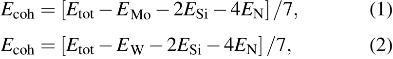
When a metal and a semiconductor are joined to form a metal-semiconductor interface, a significant charge redistribution behavior can be observed as a result of the overlap of wavefunctions from two layers. To further investigative the charge transfer between monolayer MSN and monolayer graphene and between WSN and monolayer graphene,we calculate the plane-averaged differential charge density of heterojunctions. And the plane-averaged differential charge density∆ρfor MSN and WSN are defined,respectively,as

whereρvdW,ρMSN,ρWSN,ρgrapheneare the plane-averaged charge densities of the MSN/graphene or WSN/graphene heterojunction, isolated MSN single layer, isolated WSN layer,and isolated graphene layer. As shown in Figs.5(a)and 5(b),it can be obviously observed that two diagrams show that they are similar to each other to a high degree. In regard to the reasons for this similarity, we can sum them up in three points:(i)the septuple-layered structures reduce the contact between the inner heavy atomic layer and the outer graphene layer;(ii) the electronic states of the CBM and VBM are mainly from the contributions of inner heavy core atoms(Mo and W atoms)rather than two outermost Si and N atoms;(iii)we only study the charge transfer properties between two layers but not in each monolayer. Hence, the atomic layer that contacts graphene plays a crucial role in determining the charge transfer properties and two configurations have almost equal quantity of charge transferring at the interfaces. We also notice that the charge densities around the graphene are no longer zero,which implies that although the interactions at the interface are weak,there is still charge transferring between graphene and MSN or between praphene and WSN monolayer. The charges are accumulated in the MSN monolayer or WSN monolayer,and the charges are depleted in the graphene monolayer, demonstrating that there exists charge transferring from the graphene monolayer to the MSN monolayer or WSN monolayer,which leads a built-in electric field to point from graphene to MSN or WSN monolayer.
As is well known, strain is an effective way to modulate the electronic properties of vdW heterojunctions, especially SBHs of vdW heterojunctions. In our work,we apply a strain to the heterojunction along thexdirection and a strain along theydirection simultaneously,and the strain coefficientεcan be obtained from
ε=(a−a0)/a0×100%,
whereaanda0are the strained lattice constant and the unstrained lattice constant, respectively. Ifε< 1 the strain is a compressive strain, and ifε> 1 the train is a tensile strain. In our work, we performed 10 groups of experiments per heterojunction,withεvalues ranging from−10%to 10%.The projected band structures of strained MSN/graphene and WSN/graphene heterojunctions under different strains are shown in Figs. 6 and 7. It can be observed that the CBM and VBM of two heterojunctions will move under compressive strain and tensile strain.
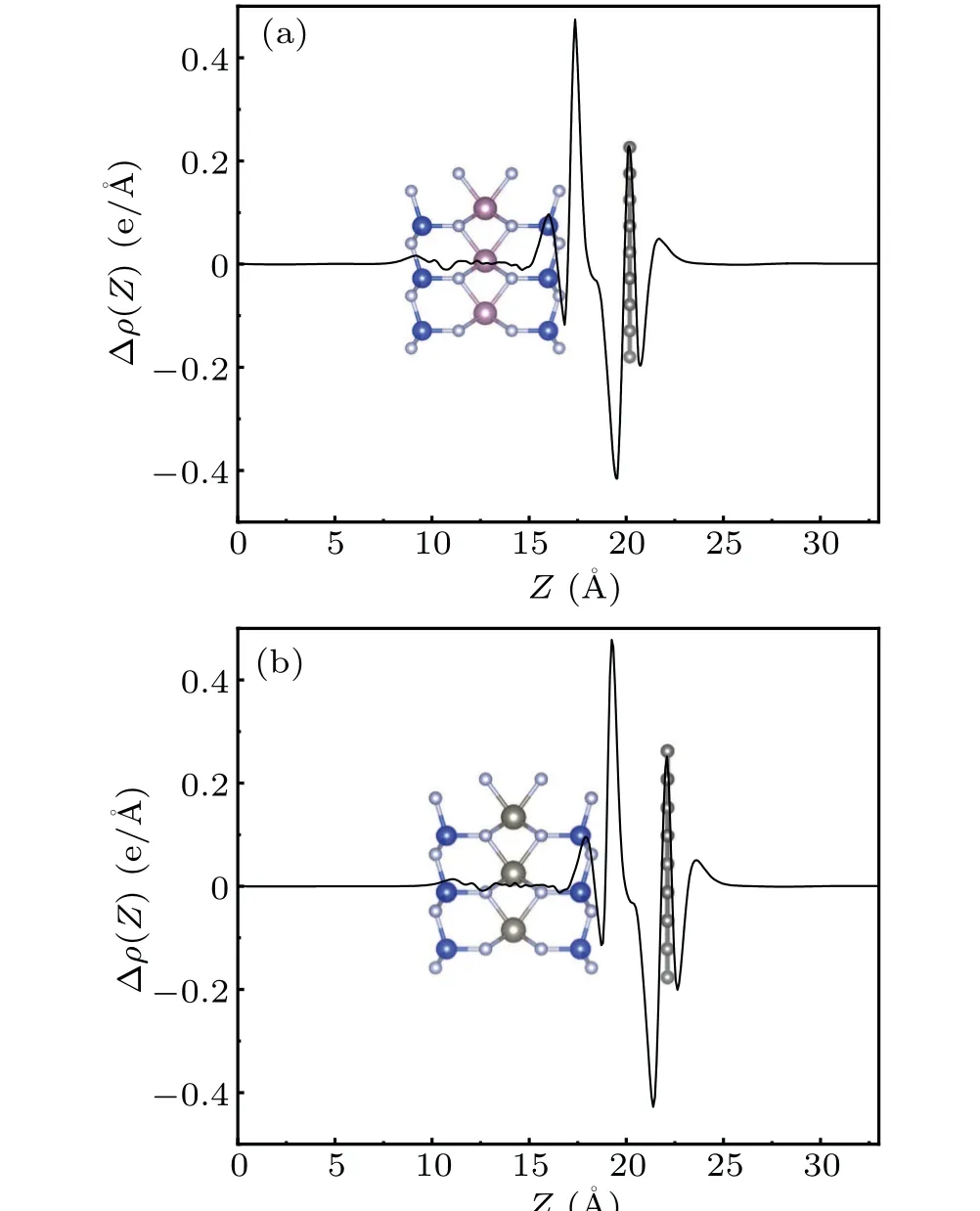
Fig. 5. Plane-averaged differential charge densities between two interfaces along vertical axis of (a) MSN/graphene heterojunction and (b)WSN/graphene heterojunction.
As seen from Fig.6,under compressive strainε=−2%,the MSN in MSN/graphene heterojunction maintains the same direct band gap characteristics under no strain.When the compression strain increases to−4%, the CBM is no longer located at the previousΓpoint but the VBM is still located at the previous point,proving that the transition from direct band gap to indirect band gap occurs with the compression strain increasing.
It can be observed from Fig.7 that unlike MSN/graphene heterojunction, the WSN is always an indirect band gap under the compressive strain in a range from−2% to−10%,which implies that the transition occurs under compressive strainε=−2%rather than−4%of MSN.We also found that under the tensile strain,the MSN or the WSN remains its original direct band gap characteristics no matter whether it is the MSN/graphene heterojunction or the WSN/graphene heterojunction.
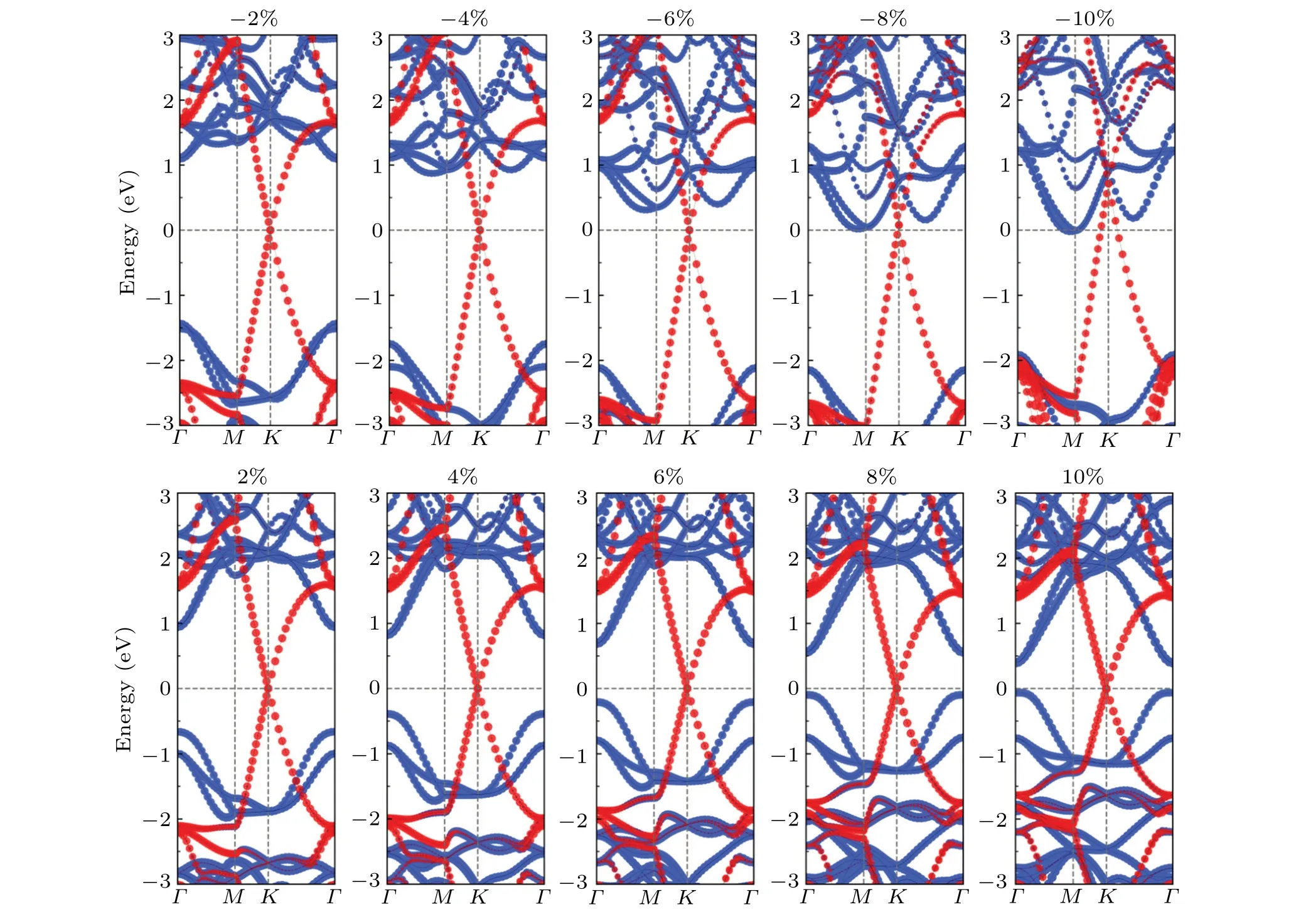
Fig.6. Projected band structures of MSN/graphene heterojunction with different values of biaxial strain ε (−10%to 10%).
The n-type and p-type Schottky barrier heights (SBHs)are calculated from

whereΦBnandΦBpare the barrier height for electrons and holes respectively.Here,ECBMandEVBMrepresent the energy of the conduction band minimum(CBM)and the valence band maximum(VBM),respectively,andEFis the Fermi energy.
Figure 8(a)shows the diagrammatic illustration of Schottky contacts and Ohmic contacts at the interface of heterojunctions. IfΦBnis smaller thanΦBp, it is said that n-type Schottky contacts are formed at the interface of the heterojunction. Similarly, ifΦBnis larger thanΦBp, it is said that p-type Schottky contacts are formed at the interface of the vdW heterojunction. WhenΦBnorΦBpdecreases to zero or further to negative, the n-type or p-type Ohmic contacts are formed. In other words,when the positions of CBM or VBM of MSN or WSN monolayer overlap with the Fermi energy level,it is said that Ohmic contacts are formed. The calculated SBHs of unstrained MSN/graphene areΦBn=1.027 eV andΦBp=0.979 eV,and the WSN/graphene areΦBn=1.557 eV andΦBp=0.776 eV, respectively. Thus, based on the above definition,the MSN/graphene and WSN/graphene heterojunctions both form p-type Schottky contacts at the interface of each heterojunction.
Furthermore,we calculated theΦBnandΦBpand plotted variation curves of barrier heights with strain, which can be seen in Figs.8(b)and 8(c). We can draw the conclusion from Fig.8(b)that when the compressive strain changes from 0 to−2%, the value ofΦBnincreases, and when the compressive strain increases from−4% to−10%, the value ofΦBnkeeps decreasing and eventually becomes negative(−22 meV).Figure 8(b) shows a decreasing trend ofΦBnunder compressive strain changing from 0 to−10%, and the minimum value is also smaller than zero(−15 meV).At this point,we claim that Ohmic contacts are formed at their interfaces. Ohmic contacts play a significant role in high-sensitively detecting the biomolecules and neural signals. When it comes to the reasons, we can attribute the transition to the fact that the electronic structure is controlled by the overlap of electron orbitals,which is strongly influenced by the magnitude of tensile strain or compressive strain. Orbital overlap behavior is found in the valence electron orbitals that dominate at the CBM and VBM in MSN/graphene and WSN/graphene heterojunctions of different atoms. Compressive strain induces the overlap of the valence electron orbitals to change, which further causes the electronic states in the conduction and valence bands to shift. When the compressive strain reaches−10%, the Fermi energy level crosses the conduction band,implying the formation of Ohmic contacts.

Fig.7. Projected band structures of WSN/graphene heterojunction with different values of biaxial strain ε (−10%to 10%).

Fig. 8. (a) Diagrammatic illustration of Schottky contacts and Ohmic contacts at the interface of heterojunctions. Variations of SBH with compressive strain and tensile strain in(b)MSN/graphene and(c)WSN/graphene heterojunctions.
On the contrary, when the tensile strain is applied, the value ofΦBnkeeps decreasing from 0 to 10%. When the applied tensile strain is increased to 10%, the valence band still lies below the Fermi energy level,proving that the Ohmic contacts have not yet been formed. When it comes to theΦBpto be considered,except under the compressive strainε=−10%,the value ofΦBndecreases from compressive strainε=−8%to unstrainedε=0% to tensile strainε=10%. The sum ofΦBnandΦBpof both MSN/graphene and WSN/graphene heterojunctions first increases from−10% to−4% and then decreases from−4%to 10%. Moreover,we also notice that for MSN/graphene heterojunction, under the compressive strain,the value ofΦBnbecomes smaller thanΦBp, implying that the Schottky contacts formed at the interface change from ptype to n-type. We observed the same phenomenon in the contact between WSN and graphene, except that it occurs at the compressive strainε=−4%. Under the tensile strain,both MSN/graphene and WSN/graphene heterojunctions remain their original p-type contacts. All these results indicate that the biaxial strain is effective to control not only the SBH but also the Schottky contacts from the n-type to the ptype and from Schottky contacts to Ohmic contacts,which are significant breakthroughs in designing novel Schottky devices based on MSN/graphene and WSN/graphene vdW heterojunctions, thereby realizing dynamic switching either between ntype and p-type Schottky contacts, or between Schottky contacts and Ohmic contacts.
Then, we plot the density of states diagrams of strained MSN/graphene and WSN/graphene heterojunctions under different strains in Fig.9. Here,for simplicity,we only plot four groups of DOS diagrams for each heterojunction at strain of−2%,−6%, 2%, and 6%, respectively. We can clearly see that under the compressive strain,the peaks around the Fermi energy level shift leftward and movements become more pronounced with compression strain increasing. Under the tensile strain,the peaks move towards the Fermi energy level. However,regardless of the compressive strain or tensile strain,the electronic states around the Fermi energy level are still mainly contributed from the Mo atoms or W atoms.

Fig.9. DOSs of(a)MSN/graphene and(b)WSN/graphene heterojunctions with different values of biaxial strain ε (−6%to 6%).
Fig.10. Schematic model of field-effect transistor based on MSN/graphene and WSN/graphene heterojunctions.
Finally,we design a schematic model of field-effect transistor as shown in Fig.10,in which both switching either between n-type and p-type Schottky contacts,or between Schottky contacts and Ohmic contacts can be realized by an external strain. In this transistor, MSN or WSN is used as the transistor channel and graphene as the metal contact. There are now a variety of practical solutions for how to induce strain in 2D materials nowadays. It has been well reported that flexible substrates can be used to apply axial tensile strains of up to 30% to graphene sheets.[36]We can use a flexible film as a substrate to induce a strain in the field-effect transistor by bending the substrate. The strain is then transferred through the substrate to the heterojunctions,resulting in tensile or compressive strain.
4. Conclusions and perspectives
In summary, we have investigated the electronic properties of MSN/graphene and WSN/graphene heterojunctions by using the first principles calculations. We can draw some conclusions below.
(i)After stacking heterojunctions,electronic properties of MSN,WSN and graphene are all well preserved in two heterojunctions. We also find a vanishingly small band gap opening in the two heterojunctions, which can be considered negligible.
(ii)The p-type Schottky contacts are formed at the interfaces of two heterojunctions. The plane-averaged differential charge density demonstrates that there exists charge transfer from the graphene monolayer to the MSN monolayer and also from the graphene monolayer to the WSN monolayer.
(iii) Applying strain is an effective way to modulate the SBHs of MSN/graphene and WSN/graphene heterojunctions.In our work, we show that when a compressive strain is applied to the heterojunction stacked by the MSN or WSN and graphene,its direct band gap can be converted into an indirect band gap;when tensile strain is applied to the heterojunction,its original direct band gap is maintained. For MSN/graphene heterojunction, when a compressive strain is applied to the heterojunction, the Schottky contacts formed at the interface change from p-type to n-type; And for WSN/graphene heterojunction,until the compressive strainε=−4%,the n-type Schottky contacts are formed.However,the application of tensile strain does not induce the transformation. Furthermore,when the compressive strain increases to−10%,the transition from Schottky contacts to Ohmic contacts is completed at the interfaces of both MSN/graphene and WSN/graphene heterojunctions.
As far as the study status ofMA2Z4monolayers andMA2Z4/graphene heterojunctions are concerned, it is of critical importance to understand their internal electronic and contact properties prior to putting those heterojunctions into practical applications in new Schottky devices. TheMA2Z4family shall bring more surprises to future electronic and Schottky devices and mayprovide more freedom for designingMA2Z4-based Schottky devices with novel functionalities. Only time will tell,but the more surprises are looming on the horizon.
Acknowledgements
One of the authors, Qian Liang, would like to thank his supervisor, Professor Quan Xie for guidance, and also his friends and colleagues for their cooperation.Project supported by the Industry and Education Combination Innovation Platform of Intelligent Manufacturing and Graduate Joint Training Base at Guizhou University, China (Grant No. 2020-520000-83-01-324061), the National Natural Science Foundation of China (Grant No. 61264004), and the High-level Creative Talent Training Program in Guizhou Province, China (Grant No.[2015]4015).

- Chinese Physics B的其它文章
- Direct measurement of two-qubit phononic entangled states via optomechanical interactions
- Inertial focusing and rotating characteristics of elliptical and rectangular particle pairs in channel flow
- Achieving ultracold Bose–Fermi mixture of 87Rb and 40K with dual dark magnetic-optical-trap
- New experimental measurement of natSe(n,γ)cross section between 1 eV to 1 keV at the CSNS Back-n facility
- Oscillation properties of matter–wave bright solitons in harmonic potentials
- Synchronously scrambled diffuse image encryption method based on a new cosine chaotic map