
Radiation effects of electrons on multilayer FePS3 studied with laser plasma accelerator
2022-08-31 09:57MengPeng彭猛JunBoYang杨俊波HaoChen陈浩BoYuanLi李博源XuLeiGe葛绪雷XiaoHuYang杨晓虎GuoBoZhang张国博andYanYunMa马燕云
Chinese Physics B 2022年8期
Meng Peng(彭猛) Jun-Bo Yang(杨俊波) Hao Chen(陈浩) Bo-Yuan Li(李博源)Xu-Lei Ge(葛绪雷) Xiao-Hu Yang(杨晓虎) Guo-Bo Zhang(张国博) and Yan-Yun Ma(马燕云)
1Department of Physics,National University of Defense Technology,Changsha 410072,China
2College of Physics and Optoelectronic Engineering,Shenzhen University,Shenzhen 518000,China
3Key Laboratory for Laser Plasmas(MoE),School of Physics and Astronomy,Shanghai Jiao Tong University,Shanghai 200240,China
4College of Advanced Interdisciplinary Studies,National University of Defense Technology,Changsha 410073,China
Keywords: space radiation,laser–plasma interaction,two-dimensional material,Raman spectroscopy
1. Introduction
Space radiation is one of the substantial threats to spacecraft and satellites because it can severely damage solar cells and electronics onboard.[1]With the continuous deepening of human space exploration, the demands on spacecraft performance are increasing. All space agencies around the world are constantly developing various countermeasures to deal with this threat. Space radiation, which has a plenitude of different types and origins,can be extremely versatile. Space radiation is usually composed of various particles, such as electrons,protons,ions,and photons. Moreover,the energy spectra of radiation belt are very broadband,spanning multiple orders of magnitude.[1,2]Space radiation belts exist in the five strongly magnetized planets in solar system, namely, Earth,Jupiter, Saturn, Uranus, and Neptune.[3–5]According to the model based on the measurements of Pioneer and Voyager detections, the electron energy in Jupiter’s radiation belt can reach 100 MeV,which is much higher than that in Earth’s radiation belt.[5–8]
In planetary radiation belts, energetic electrons are accelerated to form directional spectra fluxes characterized by a power-law or exponential decline towards higher energies.In contrast to space radiation,laboratory’s space radiation test facilities characterized by linacs or cyclotrons cannot produce broadband spectra, but instead monoenergetic beams,resulting in completely different energy deposition on the device.[9]Based on the chirped pulse amplification(CPA),[10]today’s laser system can generate power up to petawattregime to produce relativistic electron beam by laser–plasma interaction.[11,12]Electron beams with low energy divergence and exponential energy distribution emitted from laser-plasma accelerator (LPA) are similar to the conditions in space radiation, contributing to a booming research field, especially in the field of space radiation.[2,8,12]LPA is a workable advanced tool as a complementary source for space radiation testing. In 2017, Hiddinget al.[2]used LPA to reproduce the broadband Van-Allen belt level electron beam for systematically exploring the degradation of optocouplers,and a significant electronics degradation characterized straightforwardly by the current transfer ratio was acquired with such laboratory-made space radiation.
The harsh radiation environment has a severe impact on the reliability of conventional silicon-based devices. The undesirable phenomena such as single event effect, total dose effect, and displacement damage, can adversely affect their performance.[13–16]Now, quantum tunneling is setting a hard limit for further miniaturization of silicon-based electronics at nanoscale technology nodes, but the adoption of novel material and/or device structure is considered beyond this limit. Of particular interest is the two-dimensional (2D) material such as graphene,[17–20]transition metal dichalcogenide(TMD),[21–23]and black phosphorus(BP).[24–26]Their intrinsically large specific area,low power requirement,and chemical stability make devices based on 2D material a promising candidate for space instrumentation.[14]The 2D materialbased integrated electronics have a smaller sensitive volume, demonstrating stronger protection against single event effects.[27]However, zero bandgap limits the application of graphene in the field of optoelectronics.[17,18]BP(0.3 eV)and TMD(<2.0 eV)have a small bandgap that hinders the potential optoelectronic application at higher energy. Recently, 2D layered metal phosphorus trichalcogenides (MPS3,M=Fe,Ni, Mn, Zn, etc.)[28–31]have received enormous attention for the excellent electronic, optical and magnetic properties derived from their electronic structure and energy band. In this article, we study the exponential energy electron beam produced by LPA for the 2D material(FePS3)testing,which has potential space application. A series of characterizations have been performed on the FePS3sample before and after electron radiation for radiation damage analysis, and the detailed discussion and conclusion are given in Section 3.
2. Experimental details
2.1. Preparation and characterization of FePS3

Fig.1. (a)Schematic crystal structure of FePS3. (b)Brightfield microscope image of cleaved sheet samples exfoliated onto an oxidized silicon substrate.(c)AFM topography image of FePS3 sample,and the height profiles along line A.(d)The typical Raman spectrum of FePS3 sample showing Eu,E(3)1g,A(11g),E(14g),A(12g),Si-2TA,and Si-TO peaks.
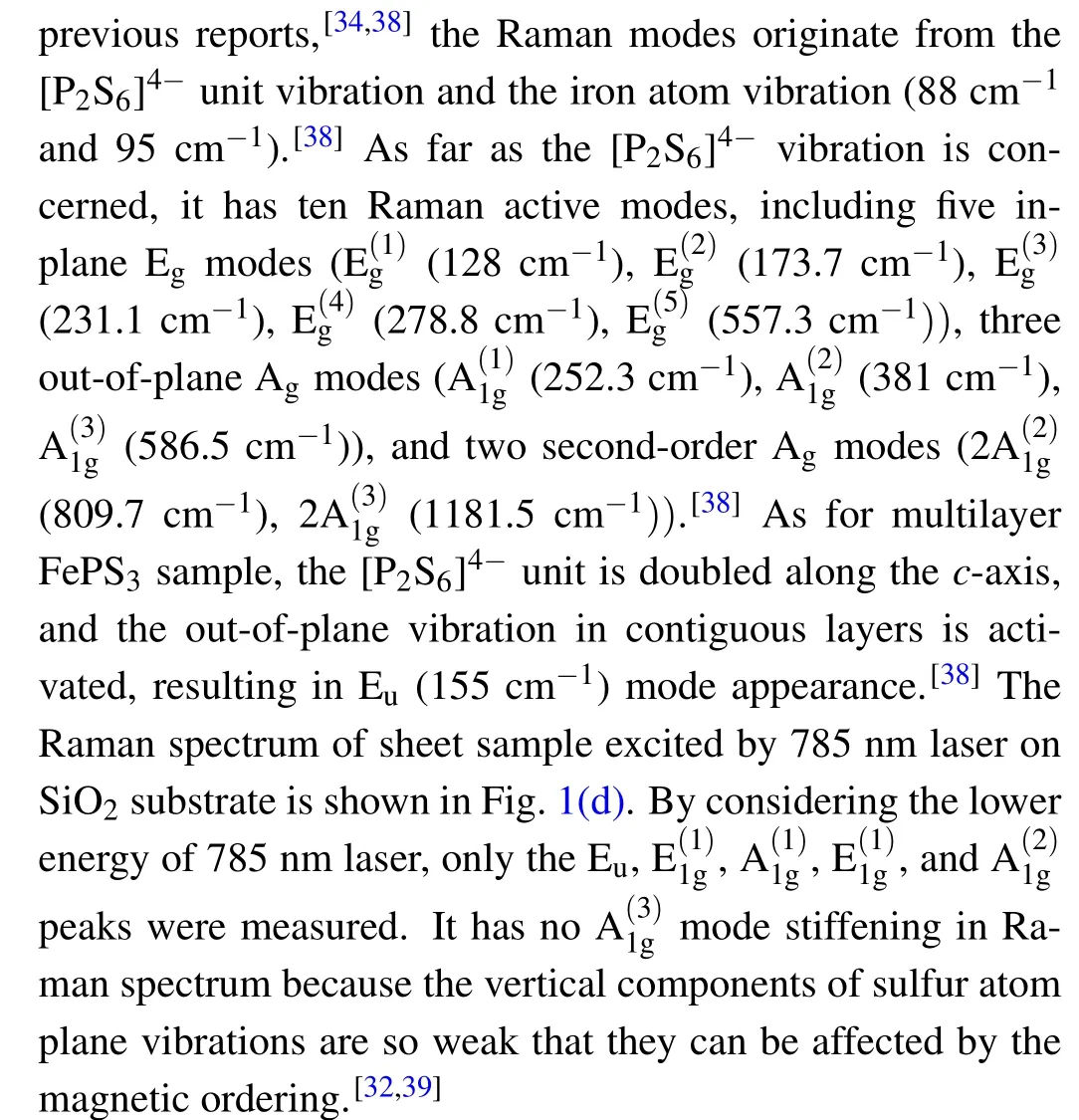
An optical microscope (BX41M-LED, Olympus) has been used to characterize the FePS3samples. In the case of exfoliated FePS3samples, the region edges and boundaries between different layers often run in parallel or are arranged at angles close to 60◦and 120◦[34](see Fig. 1(b)).This observation is due to the crack-propagation along the crystal axis of high-symmetry during exfoliation. The FePS3samples comprising areas of tens of layers with 2–20 µm lateral dimensions have been scanned by the atomic force microscopy (AFM, NT-MDT Solver SPM &SNOM). Figure 1(c) presents the AFM topography image along height profiles. Raman spectroscopy (Senterra, Bruker), as a nondestructive characterization technique, has been used to test the property of FePS3at room temperature. According to
2.2. Electron radiation
In 1979, laser electron acceleration was proposed by Tajima and Dawson.[40]In their theory, when an intense focused laser pulse(I ≥1018W/cm2)propagates through the underdense plasma, this plasma will excite a relativistic plasma wave with a field amplitude of 100 GV/m. This plasma wave passes through the plasma at the same speed of laser.[12,41]Massive charge displacements cause a high electric wake-field for electron acceleration to relativistic energy in a very short distance. The radiation damage experiment has been performed with a compact state-of-the-art Ti:sapphire laser system at Shanghai Jiao Tong University.[42]Here,the laser pulse with an energy ofE ∼5.8 J was delivered in 29 fs over a 30µm diameter focus. The laser was focused on a gas-jet target by off-axis parabola (OAP) where the gas-jet ejected the mixed gas (0.5% N2+99.5% He) at each shot to produce a broadband electron beam by self-truncated ionization injection.[42]The whole experimental process was carried out in a vacuum chamber,as described in Fig.2.
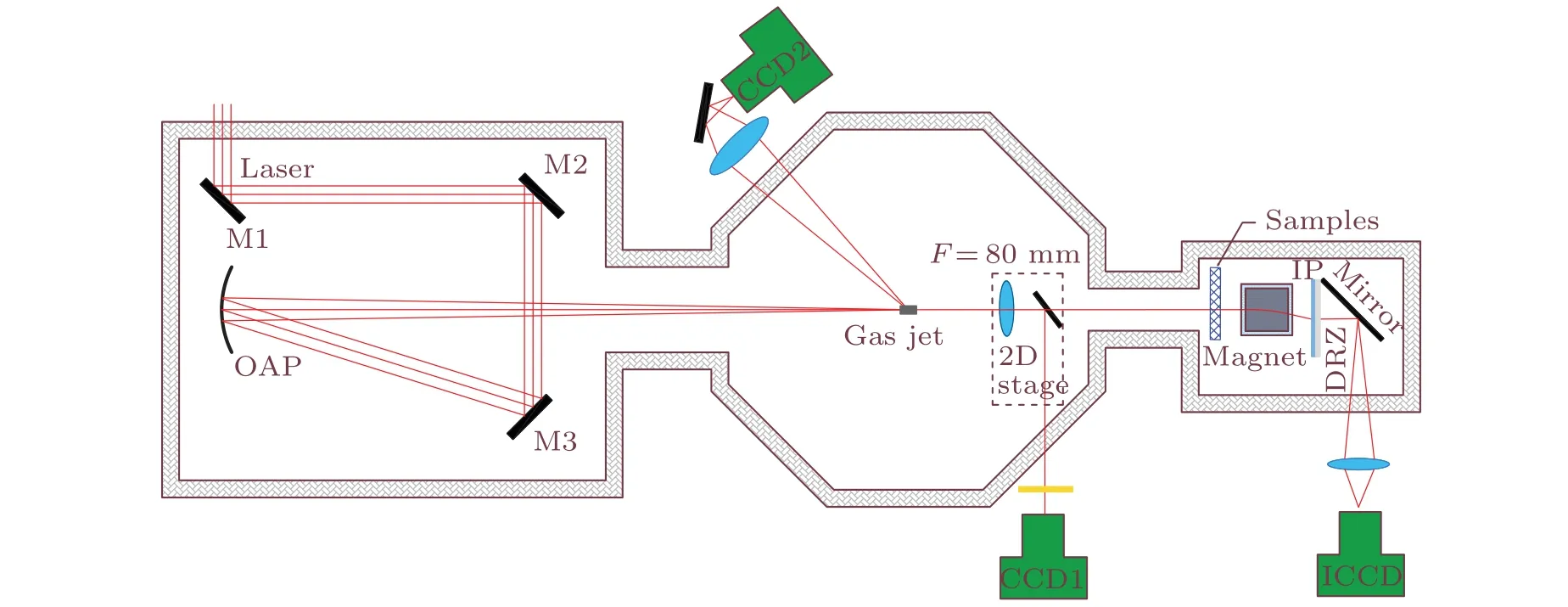
Fig.2. The setup of the radiation chamber for online monitoring electron beam. The indent laser system was strongly focused on the gas jet by OAP where the radiation was produced. Focus diagnostic microscope objective(2D stage),permanent magnet-based spectrometer,IP,and DRZ in the forward direction were positioned next to the gas jet.
An infrared camera(CCD1, Spiricon OPHIR Photonics)and 2D stage were used to monitor dynamically the focused laser spot when adjusting the laser path to maximize the laser intensity on the gas jet. The top-view image of plasma channel formed by laser–plasma interaction was captured by a 12-bit CCD camera (CCD2, Pixelfly). The electron beam was recorded by the magnetic spectrometer which consists of a permanent dipole magnet,an Image Stack(IP,Fusji),a scintillator screen (DRZ, Mitsubishi Chemical), and an intensified charge-coupled device (ICCD, Andor) camera. The dipole magnet was 16 cm long, 1.0 T magnetic field strength with a 1 cm gap. The direction of magnetic field in the gap was perpendicular to its horizontal plane during installation. The distance between the exit of dipole magnet and the IP was 16.5 cm, which fully resolves the peak electron energy up to∼400 MeV.The energetic electron flux could penetrate the IP to image on the DRZ,and then the fluorescence signals emitted from DRZ were recorded by ICCD online. A cumulative electron signals with 5 shots in IP are presented in Fig. 3(a).Based on the gyroradius of the electron trajectory in dipole magnet and electron signals recorded by IP, an average electron number of 1.2×10⁷per shot is produced. The fluence of LPA-produced electron beam per shot is approximately equivalent to the electron beams with energies greater than 0.2 MeV in Earth’s radiation belt. The broadband electron spectrum is depicted in Fig.3(b)(black line).
In order to make FePS3samples with cross-section of about 1×1 cm fully irradiated by an electron beam with a few milliradian divergence,an 8 mm thick aluminum foil has been used to enlarge the electron beam spot. Meanwhile, an InSe film has been used to monitor the uniformity and spot size of the electron beam,while the magnetic spectrometer and DRZ were positioned in the front of FePS3sample for dynamic monitoring electron beam.The schematic diagram of radiation test is depicted in Fig. 4(a), where the accumulated electron beams with 3 shots were irradiated on the FePS3samples. The transportation process of energetic electron beam in aluminum foil has been simulated with Geant4 (Version 4.10.7).[43,44]The“FTFP BERTGE”physics package was used to describe the transportation of energetic electrons and secondary particles. It was assumed that a plane particle source of 1 mm radius,50 milliradian divergence degree shot electrons to aluminum foil after 50 cm flight in vacuum. Based on the simulation results,the spot radius of the outgoing electron beam was expanded to 5 mm, fully covering the surface of testing samples(see Fig.4(b)).The simulated outgoing electron spectrum is presented in Fig.3(b)(red line).
The energetic electron beams produced by LPA are well beyond the energy limit of Earth’s radiation belt where the majority of electrons have energies up to 15 MeV. However, it shall be pointed out that the most important aspect is the exponential electron spectrum produced by LPA.[12]Moreover, based on the simulation results, the deposited energies to FePS3sample via electron–nucleus scattering are rather constant for electron energy range above 3 MeV (see Fig. 5). The total absorbed dose of FePS3sample irradiated by LPA-produced electron beams is about 1.2 mGy, which is 10% higher than that produced by electron beams at geosynchronous orbit at the same electron intensity.

Fig.3. The exponential electron beam produced from LPA.(a)The raw information of electron beams obtained by IP. (b) The induced broadband electron spectra before (black line, the experimental result) and after(red line,the simulated result)passing through Al foil.

Fig.4. (a)Schematic diagram of the electron beam for radiation test. (b)The spot size of electron flux after propagating Al foil.
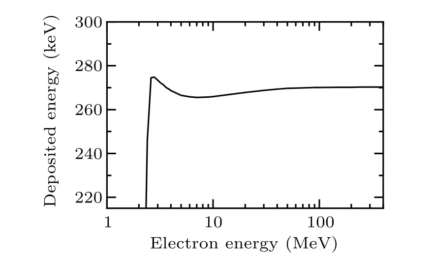
Fig. 5. The simulated results of deposited energy for electron energy from 3 MeV to 400 MeV in the FePS3 sheet sample.
3. Results and discussion
Electron stopping is mainly controlled by inelastic scattering between the incoming energetic electron beam and the electrons in the target.[45]Inelastic scattering can excite target electrons to relatively high energy(keV),which can transfer electron excitation energy away from the central region of the lattice, causing damage far away from the collision region. When the transferred energy is large enough to exceed the threshold for target atom displacing from lattice position,it causes to ionization and bond breakage. Once electron beams transfer enough energy, or numerous inelastic scatterings occur close to each other, the cascade process develops into a complex multi-body phenomenon,leading to the lattice breakup. The region of overlapping collisions can be regarded as “hot”, called a “heat spike”,[46–48]which may lead to intense heating of crystal lattice and damage to the cylindrical heat spikes.[49]Near the sample surface, the heat spike can lead to massive sputtering evaporation.[50]The optical image of InSe film exposed to the energetic electron beam is presented in Fig. 6(a). There are significantly light spots corresponding to the thinner area formed from the massive evaporation,whereas the optical characteristics of InSe film also indicate that the electron flux uniformity was good after propagating Al foil. The energies transferred to the FePS3sample were much larger than the bond energy and Van Der Waals gap,causing the bond to broke and massive particle evaporation.As a result,electron radiation led to bulk sample cleavage and damage between areas of uneven thickness (see Figs. 6(b)–6(c)).
The energy of electron beam far exceeds the threshold for knock-on damage,and hole formation to the crystal lattice can be initiated at energy as low as tens of keV.[51]The optical image of sheet sample after electron radiation is presented in Fig. 7(a). It has numerous cyan holes on the FePS3surface caused by electron sputtering. The electron radiation effect on the surface topography of FePS3was also characterized with AFM at ambient temperature,while the surface image and the height information of multilayer FePS3sample following radiation are shown in Figs.7(b)–7(c). The thin sheet sample has smaller average roughness (Ra) than the thick sample, which is ascribed to more average energy acquired by sample target atoms during radiation and impurities on the surface. During the preparation of sheet samples, H2O and O2molecules adhere inevitably to the sample surface. Electron radiation breaks the structure of [P2S6]4−, and the dangling bonds of S and P can combine H2O and O2molecules to form S=O and P=O bonds.

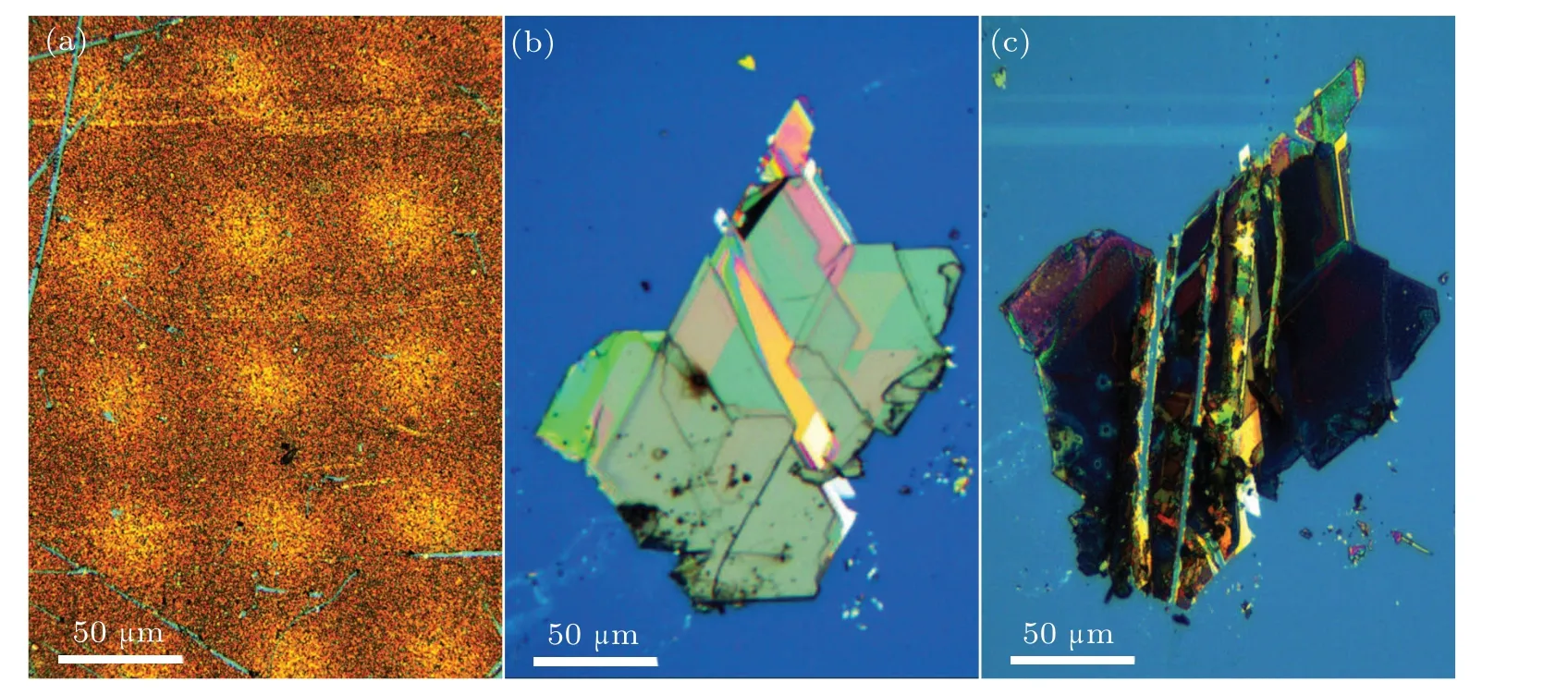
Fig.6. (a)Optical image of InSe with obvious light spots after radiation. (b)Optical image of bulk FePS3 sample before radiation. (c) The electron-induced cleavage of bulk FePS3 sample after radiation.
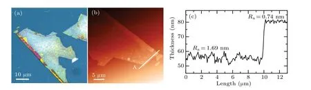
Fig. 7. (a) Brightfield microscope image of sheet samples after electron radiation. (b) AFM surface topography of FePS3 sheets following energetic electron radiation. (c)The cross-sectional height along line A in(b).
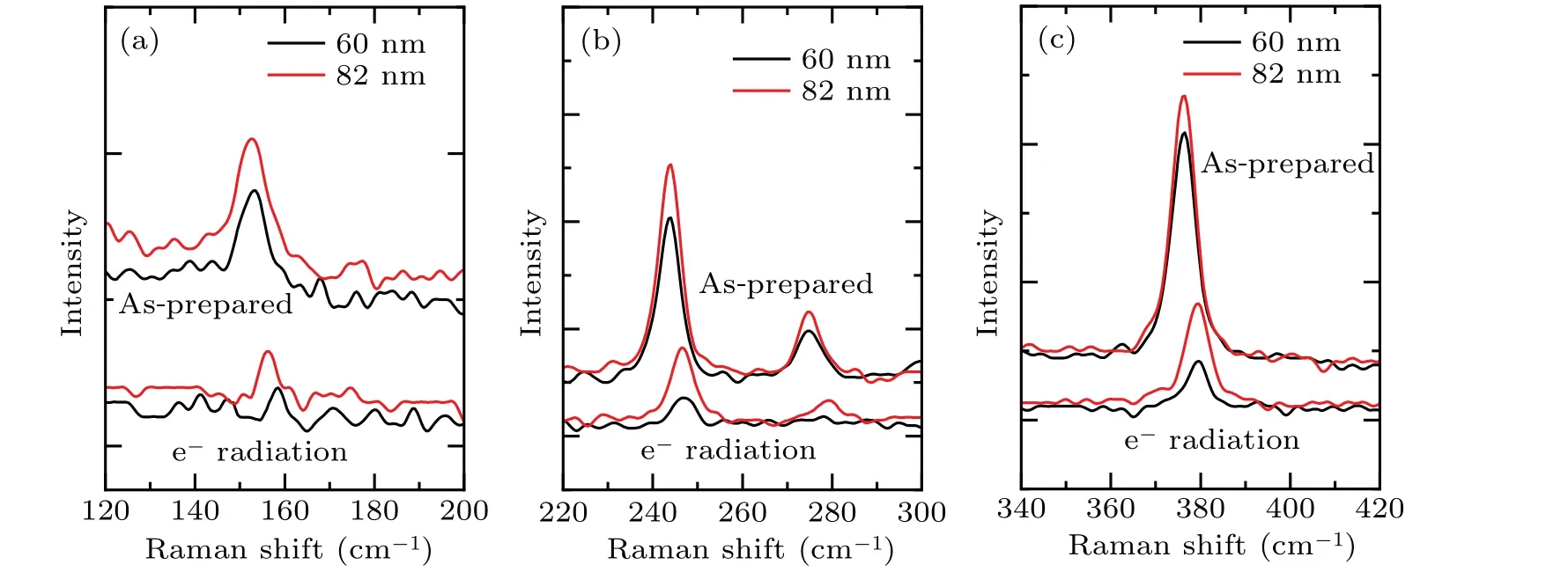
Fig. 8. The Raman spectra of FePS3 sample before and after electron radiation. (a) Out-of-plane vibration: Eu mode. (b) Out-of-plane vibration: A(11g) mode and in-plane vibration: E(14g) mode. (c)Out-of-plane vibration: A(12g) mode.
4. Conclusion
In combination with the established conventional radiation source, LPA, as a complementary radiation source, can allow us to reproduce space radiation for electronic tests. In this work, a compact state-of-the-art Ti:sapphire laser system at a laser intensity ofI=2.8×10¹⁹W/cm2has been used to produce broadband electron beams for studying space radiation effects on the 2D material. In this experiment of laserplasma interaction,we have produced an exponential energetic electron beam with an average intensity of 1.4×10⁷/shot.
The effects of electron beam radiation on tens of layers FePS3samples have been systematically investigated with different kinds of characterization tools. Electron radiation led to the bulk sample cleavage and damage between areas of uneven thickness, while the energetic electron beam caused massive sputtering and ablation of the FePS3sheet sample, resulting in the surface of FePS3samples rough dramatically. Electron radiation also caused severe damage on the bipyramid structure of[P2S6]4−unit and the cleavage of P–P and P–S bonds,resulting in all the characteristic peaks sharply weakened to some extent, or even disappearing. It has a radiation threshold on the 2D material and device for normal operation under such harsh electron radiation. Our results pave the way towards testing the property of 2D materials under intense radiation and the allowable radiation dose for the application of 2D material and device.
Acknowledgements
Project supported by the National Natural Science Foundation of China (Grant No. 11975308), the Strategic Priority Research Program of Chinese Academy of Sciences (Grant No. XDA25050200), and Science Challenge Project (Grant No.TZ2018001).
猜你喜欢
今日农业(2022年15期)2022-09-20
Plasma Science and Technology(2022年7期)2022-08-01
娃娃乐园·绘本(2021年9期)2021-09-13
诗潮(2019年11期)2019-11-23
红楼梦学刊(2019年2期)2019-04-12
大众文艺(2019年3期)2019-01-24
学校教育研究(2018年1期)2018-10-21
电子技术与软件工程(2016年24期)2017-02-23
商业文化(2016年16期)2016-09-05
扬子江诗刊(2015年3期)2015-11-14

- Chinese Physics B的其它文章
- Direct measurement of two-qubit phononic entangled states via optomechanical interactions
- Inertial focusing and rotating characteristics of elliptical and rectangular particle pairs in channel flow
- Achieving ultracold Bose–Fermi mixture of 87Rb and 40K with dual dark magnetic-optical-trap
- New experimental measurement of natSe(n,γ)cross section between 1 eV to 1 keV at the CSNS Back-n facility
- Oscillation properties of matter–wave bright solitons in harmonic potentials
- Synchronously scrambled diffuse image encryption method based on a new cosine chaotic map