
Synthesis of hexagonal boron nitride films by dual temperature zone low-pressure chemical vapor deposition
2022-08-31 09:57ZhiFuZhu朱志甫ShaoTangWang王少堂JiJunZou邹继军HeHuang黄河ZhiJiaSun孙志嘉QingLeiXiu修青磊ZhongMingZhang张忠铭XiuPingYue岳秀萍YangZhang张洋JinHuiQu瞿金辉andYongGan甘勇
Chinese Physics B 2022年8期
Zhi-Fu Zhu(朱志甫) Shao-Tang Wang(王少堂) Ji-Jun Zou(邹继军) He Huang(黄河)Zhi-Jia Sun(孙志嘉) Qing-Lei Xiu(修青磊) Zhong-Ming Zhang(张忠铭)Xiu-Ping Yue(岳秀萍) Yang Zhang(张洋) Jin-Hui Qu(瞿金辉) and Yong Gan(甘勇)
1School of Information Engineering,Zhengzhou University of Technology,Zhengzhou 450044,China
2Engineering Research Center of Nuclear Technology Application(East China University of Technology),Ministry of Education,Nanchang 330013,China
3State Key Laboratory of Particle Detection and Electronics,Institute of High Energy Physics,Chinese Academy of Sciences,Beijing 100049,China
4Engineering Department,Lancaster University,Lancaster,LA14YW,United Kingdom
Keywords: ammonia borane,dehydrogenation,h-BN,dual temperature zone
1. Introduction
Hexagonal boron nitride (h-BN), SiC, and diamond[1,2]are representatives of the third-generation wide-bandgap semiconductor materials. The h-BN is a white crystal, and its crystal structure is very similar to graphite, so the h-BN is also called “white graphite”. The h-BN has attracted much attention due to its high-temperature resistance,low coefficient of thermal expansion, high thermal conductivity, low dielectric constant, reliable electrical insulation,and excellent optical properties.[3]It has important applications in thermal conductivity,[4]high-temperature oxidationresistant coating,[5]photoelectric devices,[6]graphene electronic devices,[7]nuclear radiation detection,[8]and other fields.[9,10]
There have been various methods to synthesize h-BN,such as mechanical exfoliation, liquid-phase exfoliation, and chemical vapor deposition.[11]Among them, chemical vapor deposition (CVD) is a technique for growing large-area film with low manufacturing cost. The chemical vapor deposition synthesis of h-BN has also been reported. For example, with Ni,[12]Cu,[13]Pt[14]or Si/SiO2[15]used as the substrates, the h-BN films are synthesized by LPCVD or APCVD.
At present,the growth of h-BN films by CVD is developing mainly toward two directions: the first growth direction is for growing two-dimensional materials(single layer or several atomic layers of h-BN films)and the second growth direction is for growing thick films,which is used to fabricate semiconductor devices.
There are many precursors for the synthesis of h-BN thin films by CVD,such as ammonia(NH3)and boron trichloride BCl3,[16]triethyl borane (TEB) and ammonia (NH3),[17]diborane (B2H6) and ammonia (NH3),[18]urea (CH4N2O) and boric acid(H3BO3),[19]borazine,[20]ammonia borane,[21]etc.However, due to the toxicity of BCl3, TEB, H3BO3, B2H6,etc.,and the flammability of borazine,the ammonia borane is chosen as the precursor to prepare BN thin films in this work.
For applications such as nuclear radiation detection and optoelectronic devices, the high-quality large-area and thick h-BN films are required,which still faces huge challenges. In addition, the temperature has a great influence on the synthesis of thin films by CVD.Growth at low temperatures is limited by chemical reactions, and at high temperatures, growth is limited by decomposition. Therefore,the temperature field is very important for the synthesis of h-BN films,and there is still a lack of research in this aspect. In this work,we use solid ammonia borane as the precursor to study the synthesis of h-BN on the surface of the sapphire substrate under low-pressure condition. The h-BN film grown on a catalytic metal substrate needs to be transferred. Whereas, the direct epitaxial growth of h-BN on non-catalyzed sapphire substrates more efficiently obtains wafer-scale h-BN and overcomes the surface damage and organic contamination that occurs during transfer. The synthesis of h-BN film is carried out in a tube furnace with a dual temperature zone,and the effect of dual temperature zone on the growth rate of the film and the quality of the film crystal are studied. This study will provide an experimental basis for growing large-area high-quality h-BN films.
2. Experimental process
In this study,h-BN films were synthesized by the LPCVD method. As shown in Fig. 1(a), the precursor ammonia borane was heated by an independent box furnace,and using Ar as the carrier gas, the product of the thermal decomposition of ammonia borane was introduced into a dual temperature zone high-temperature tubular furnace for BN film growth. As shown in Fig.1(b),five different positions were taken to study the influence of the dual temperature zone on the film growth rate and the film crystal quality.Positions 1 and 5 were located in the center of the two high-temperature zones,respectively.
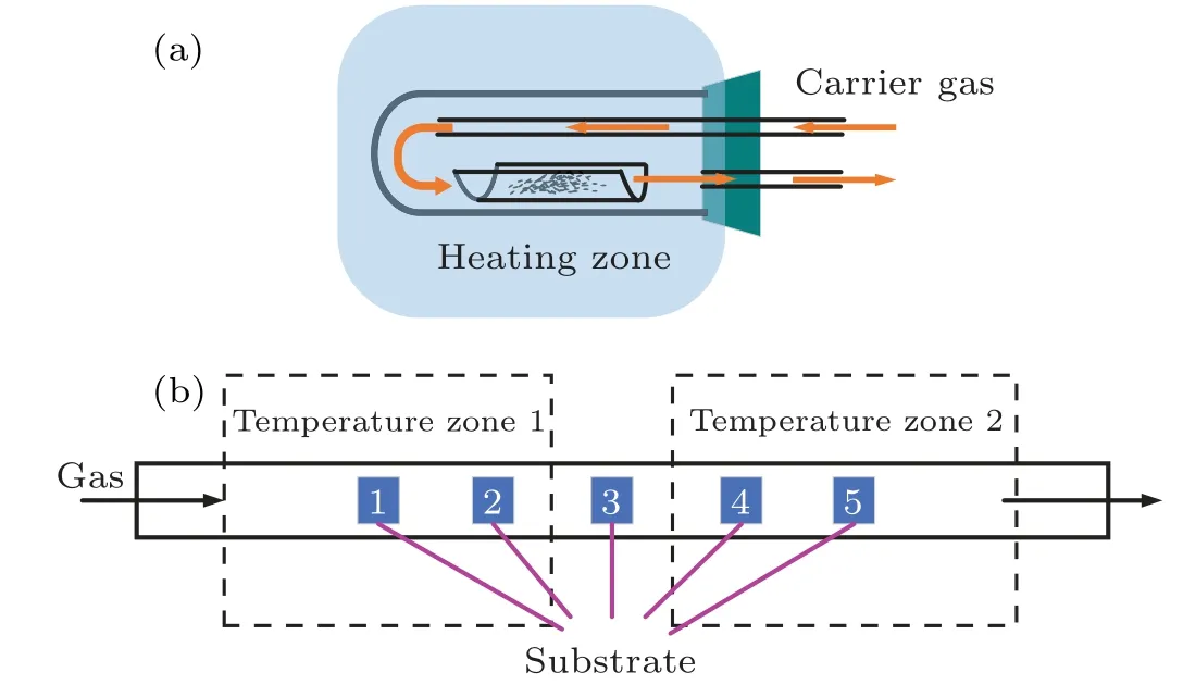
Fig.1. Schematic diagram of(a)precursor heating device and(b)five substrate positions in the dual temperature zone.
The substrate used in the experiment was 1 cm×1 cmcplane(0001)sapphire(Al2O3). First,the five substrates were ultrasonically cleaned with acetone, anhydrous ethanol and deionized water for 10 min,and then the substrates were taken out and dried with nitrogen (N2), placed in the sample boat and sent to the 5 positions as shown in Fig.1(b)sequentially,the constant temperature length of the two temperature zones was 290 mm,the distance between each substrate was 80 mm,and the substrate 1 and substrate 5 were located in the center of two temperature zones respectively. Then, the reaction chamber was evacuated to below 1 Pa to remove the air in the tube furnace. The heating was started through programmed control,and N2(80 sccm)was introduced. The two temperature zones of the tube furnace were heated to 1250◦C. After the temperature reached 1250◦C,30-min-annealing was performed to remove oxides on the surface of the substrate. After 1000 mg of ammonia borane was placed into an independent box furnace(KSL-1100X),heating was started,and the heating temperature rose up to 120◦C, while 20 sccm of Ar as the carrier gas was passing through the decomposed product of ammonia borane into the tube furnace, and N2flows in at the same time. with the growth pressure maintained at 500 Pa.After the growth ended,the tube furnace temperature was lowered to room temperature with the help of 50-sccm N2gas flow,and finally the samples were taken out.
The surface morphology and thickness for each of the h-BN films were characterized by scanning electron microscopy(SEM, Zeiss Merlin Compact). The elemental composition and quantitative analysis of the film were determined by xray electron spectroscopy (XPS, Bruker D2 PHASER). The crystal structure and composition of the film were characterized by an x-ray diffractometer (XRD, Thermo Scientific Escalab 250Xi). In this work, an atomic force microscope(AFM, Bruker Dimension XR) was used to characterize and analyze the surface roughness of the h-BN film. In this work, the transmittance and absorptivity of h-BN film were tested by ultraviolet-visible spectrophotometry (UV-Vis, Agilent Cary 60). In this work, Raman spectroscopy (Raman spectra, Thermo Scientific DXR2) was used to characterize the material composition and crystal quality of the film. In addition,Fourier transform infrared spectroscopy(FTIR)was used to characterize the chemical bonds present in the sample and the chemical structure of the molecule of the film sample.
3. Results and discussion
First, the chemical states of the grown film samples are characterized by XPS,the characterization results of sample 2 are shown in Figs. 2(a) and 2(b). The XPS results show that the binding energy(BE)values of B and N are 190.49 eV and 398.16 eV, respectively, corresponding to the B–N bond.[22]This also proves that the synthesized films are BN films. The degree of dehydrogenation of NH3–BH3is related to the pyrolysis temperature and time,and incomplete dehydrogenation at lower growth temperatures will result in some H atoms remaining to form a small amount of BNH polymer,which shifts the binding energy to the lower energy region. Therefore,the B and N binding energy peaks of the h-BN film samples are slightly lower than the 190.98 eV and 398.78 eV of the single crystal h-BN film.
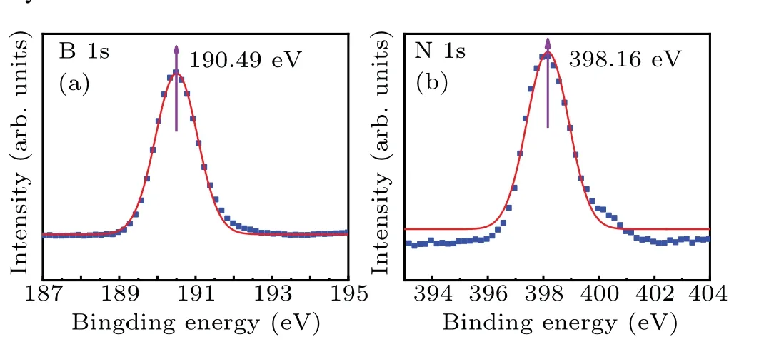
Fig.2. All five samples presented consistent XPS results of(a)B 1s spectra and(b)N 1s spectra.
The crystalline quality for each of the h-BN sample films is characterized by Raman scattering spectroscopy. As shown in Fig. 3, the five film samples each have a Raman scattering peak at 1366.9 cm−1,which corresponds to the E2gvibration mode of the B–N bond in the h-BN film,which indicates that the synthesized film is h-BN film with hexagonal phase.Compared with the peak of 1365 cm−1for a single crystal h-BN, the peaks of the samples are shifted towards the highfrequency direction, which is caused by the in-plane tensile stress generated by the lattice mismatch between the sapphire substrate and the h-BN film. The analyses of the full width at half maximum (FWHM) of the five samples show that all samples but for sample 1 have relatively good quality. It may be due to the fact that when the precursor is transported to the No.1 position,the dehydrogenation is not complete,resulting in a relatively poor film quality; and as the precursor transport process goes on,the degree of dehydrogenation becomes higher and higher,and the quality of the subsequent films turns relatively good.
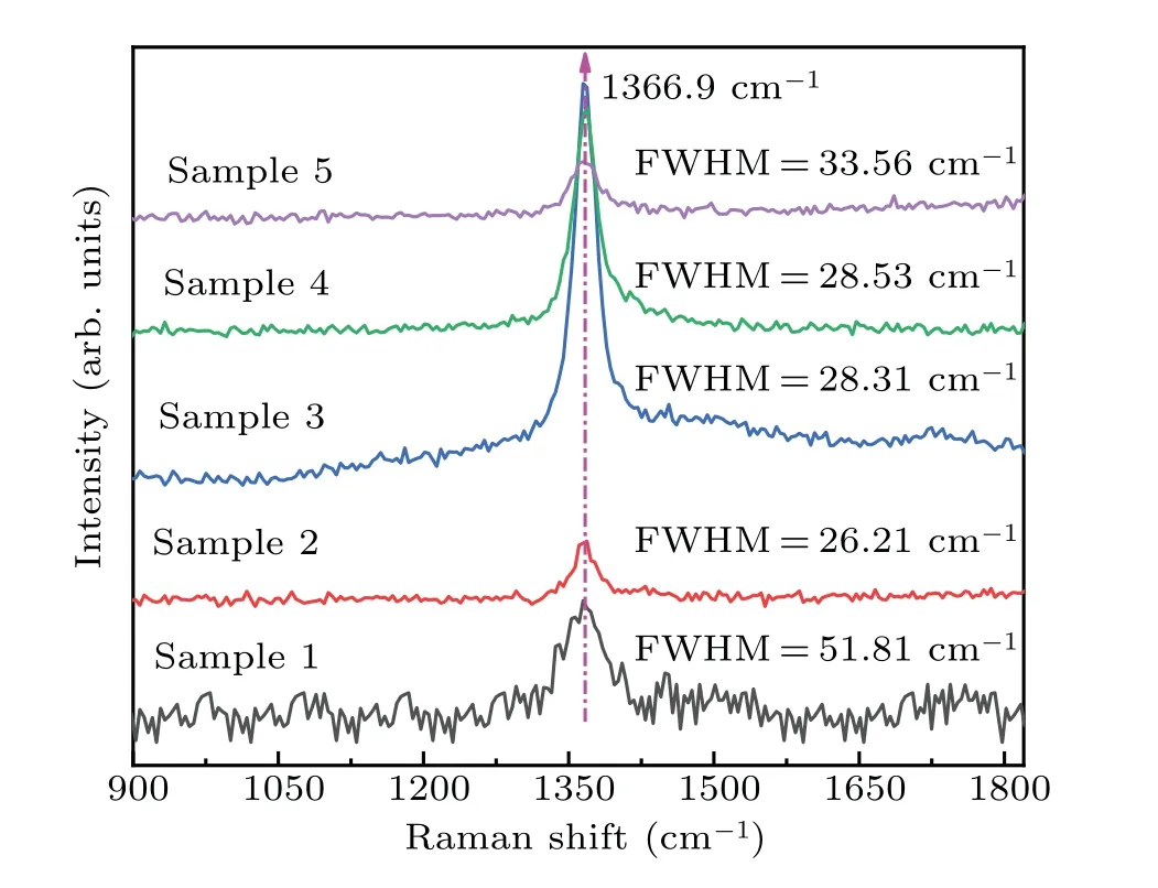
Fig.3. Raman spectra of five samples in dual temperature zone.
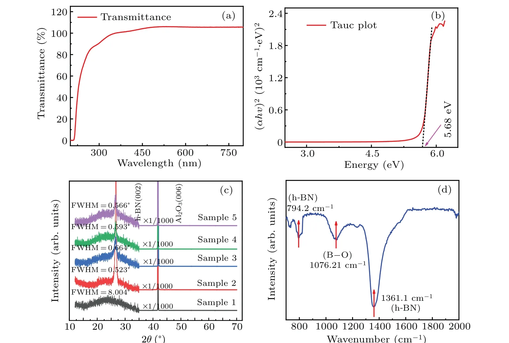
Fig. 4. (a) Transmission spectrum of film sample, (b) curve of (αhv)2 versus photon energy, (c) XRD diffraction patterns of fvie samples in dual temperature zone,and(d)FTIR spectrum of film sample.
The optical properties of sample 2 are characterized by UV-Vis spectrophotometer. As shown in Fig.4(a),the change of the transmittance of the sample film with the incident wavelength is tested, and the transmittance of the sample is close to 100% in the visible light region, indicating that the surface of the film sample is relatively flat and the quality of the film crystal is good. There is a steep absorption edge at 210 nm,which corresponds to h-BN.According to the fitting formula of the bandgap width of the direct bandgap semiconductor,by extending the tangent of the curve of(αhv)2versusphoton energy. The value of the intersection with the photon energy axis is the corresponding optical bandgap as shown in Fig. 4(b). The optical bandgap of the sample is 5.67 eV,which is consistent with the experimental value reported by others.[23]The crystal structure of the synthesized h-BN film was characterized by XRD.The XRD results of the five sample films in the dual temperature zone are shown in Fig.4(c).The diffraction peak near 41.77◦is from the Al2O3(006)plane diffraction,while the diffraction peak near 26.65◦comes from h-BN(002) plane diffraction. Sample 1 at position 1 in the dual temperature zone has only one broad peak, which may be due to the poor crystal quality caused by incomplete dehydrogenation. As the precursor continues to transport, the dehydrogenation is more complete, so the remaining 4 samples have relatively sharp diffraction peaks. The XRD peaks shown in Fig.4(c)are further analyzed by the full width at half maximum (FWHM), and it is found that the FWHM of sample 1 is significantly higher than those of the other samples,which indicates that all samples but for sample 1 have relatively good quality. Since the center of the diffraction peak is located at 26.65◦, the interplanar spacing calculated from the Bragg diffraction formula (2dsinθ=nλ) is 0.3344 nm,which is principally consistent with the 0.3328-nm interplanar spacing of single-crystal h-BN(002), confirming what we have synthesized is h-BN film.In addition,the h-BN film sample is also characterized by FTIR,and the results are shown in Fig.4(d).The two main bands at 794.2 cm−1and 1361.1 cm−1are attributed to B–N stretching and B–N–B bending respectively,which are typical features of h-BN,while the emission band near 1076.21 cm−1may be caused by oxygen atoms introduced in the testing process or the growth process under low vacuum.[24]
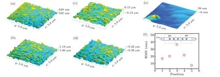
Fig.5. (a)–(e)AFM results of five samples in dual temperature zone, and(f)roughness of five samples in dual temperature zone, with inset showing positions of five samples in dual temperature zone.
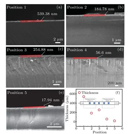
Fig. 6. (a)–(e) SEM cross-sectional views of five samples in dualtemperature zone, and (f) thickness of h-BN film varying with position in dual-temperature zone,with inset showing positions of five samples in dualtemperature zone.
The surface morphology for each of the film samples is characterized by AFM,as shown in Figs.5(a)–5(e). From the results, it can be seen that the roughness of the sample surface is closely related to the temperature. Samples 1 and 5 are located in the center of the two temperature zones respectively. The high growth temperature enhances the ability of surface adatoms to migrate, so the surface is relatively flat,while sample 3 is the farthest from the center of the two temperature zones,it has a rougher surface.The overall roughness presents the tendency of going up first and coming down second as shown in Fig.5(f).
The SEM is used to observe the thickness values of the five sample films in the dual temperature zone as shown in Figs. 6(a)–6(e), the growth rates of the five samples at five different positions are 4.49 nm/min, 1.540 nm/min,2.124 nm/min,0.472 nm/min,and 0.150 nm/min,respectively.The overall thickness shows a downward trend, as shown in Fig. 6(f), which is mainly due to the fact that with the consumption of the precursor,the precursor concentration gradually decreases and the nucleation rate decreases, resulting in a decrease in the growth rate. From the SEM results, the h-BN thin films with a thickness of 540 nm are heteroepitaxially grown on the sapphire substrates,but no h-BN film is found to be peeled off from the sapphire substrate. This situation is most likely due to the formation of a thin AlxNylayer at the interface between h-BN and Al2O3when the sapphire substrate is annealed at high temperature before h-BN growing.The nitrogen atoms in N2replace oxygen atoms on the surface of the sapphire substrate, and then form N–Al bonds at high temperatures(greater than 1200◦C).The formation of AlxNylayer reduces the lattice mismatch and thermal mismatch at the interface between h-BN and Al2O3, and thus effectively relieving the stress at the interface between h-BN and Al2O3.Therefore, we did not find h-BN peeling from the sapphire substrate in this study.
4. Conclusion
In this work, BN films are synthesized on sapphire substrates by the LPCVD method. Various characterization results confirm that the synthesized films are h-BN films with hexagonal phases. The effects of the temperature field on the growth rate and quality of h-BN films are studied through samples at five different positions in the dual temperature zone. It is found that sample 1 has poor crystal quality due to incomplete dehydrogenation, and with the gradual consumption of precursors,the growth rates of the five samples all show a general downward trend. In addition,by studying the variation of(αhv)2with photon energy,the optical bandgap of the synthesized film is 5.67 eV.This study will provide an experimental basis for growing large-area high-quality h-BN thin films.
Acknowledgements
Project supported by the National Natural Science Foundation of China (Grant No. 61964001), the Key Research and Development Program of Jiangxi Province,China(Grant No. 20212BBG73012), the Natural Science Foundation of Jiangxi Province, China (Grant No. 20192BAB207033), the Key Scientific Research Projects of Henan Higher Education Institutions, China (Grant No. 22A490001), the State Key Laboratory of Particle Detection and Electronics,China(Grant No. SKLPDE-KF-2019), and the Foundation of Engineering Research Center of Nuclear Technology Application (East China Institute of Technology)(Grant No.HJSJYB2021-4).
- Chinese Physics B的其它文章
- Direct measurement of two-qubit phononic entangled states via optomechanical interactions
- Inertial focusing and rotating characteristics of elliptical and rectangular particle pairs in channel flow
- Achieving ultracold Bose–Fermi mixture of 87Rb and 40K with dual dark magnetic-optical-trap
- New experimental measurement of natSe(n,γ)cross section between 1 eV to 1 keV at the CSNS Back-n facility
- Oscillation properties of matter–wave bright solitons in harmonic potentials
- Synchronously scrambled diffuse image encryption method based on a new cosine chaotic map