
Wake-up effect in Hf0.4Zr0.6O2 ferroelectric thin-film capacitors under a cycling electric field
2022-08-31 10:00YilinLi李屹林HuiZhu朱慧RuiLi李锐JieLiu柳杰JinjuanXiang项金娟NaXie解娜ZengHuang黄增ZhixuanFang方志轩XingLiu刘行andLixingZhou周丽星
Chinese Physics B 2022年8期
Yilin Li(李屹林) Hui Zhu(朱慧) Rui Li(李锐) Jie Liu(柳杰) Jinjuan Xiang(项金娟)Na Xie(解娜) Zeng Huang(黄增) Zhixuan Fang(方志轩) Xing Liu(刘行) and Lixing Zhou(周丽星)
1Faculty of Information Technology,Beijing University of Technology,Beijing 100023,China
2Institute of Microelectronics,Chinese Academy of Sciences,Beijing 100029,China
Keywords: wake up,HZO ferroelectric thin-film,cycling electric field,oxygen vacancy
1. Introduction
Recently, high-kdielectrics such as HfO2have been extensively implemented in the microelectronics industry. In 2011, HfO2-SiO2thin films were discovered to exhibit ferroelectric properties by B¨osckeet al.[1]HfO2exists in the form of three basic crystal structures, which are monoclinic,tetragonal and cubic. These structures are centrosymmetric and exhibit no ferroelectric polarization.[2,3]By doping HfO2with Si, Zr, Y, etc., an orthorhombic phase can be obtained.The structure exhibits asymmetric centrality,which is responsible for its ferroelectric properties.[4,5]Ferroelectric randomaccess memories using HfO2-based thin films exhibit fast read and write speeds (tens of ns), low operating voltages, and small power consumption. Furthermore, compared to traditional ferroelectric materials (such as PZT), HfO2-based thin films were compatible with existing CMOS semiconductor processes. They had a sufficiently strong polarization strength(15–45 µC/cm2) in the nanometer range (10 nm).[6–9]As a high-kmaterial, the leakage current of HfO2was low, giving it good retention properties (about 10 years).[10]This opens a new path for the development of ferroelectric field-effect transistors.[11]
A memory device undergoes continuous writing, reading, and data updating, and thus requires a ferroelectric thin film to withstand the large number of switching cycles. This brings about reliability problems, such as the wake-up effect, which refers to the increase in remnant polarization relative to the initial state at the beginning of 103–104switching cycles.[12]A number of wake-up mechanisms have been proposed, including an oxygen vacancy redistribution,[13]field-cycling-induced phase transitions,[14]and domain depinning mechanisms.[12]Oxygen vacancies play an important role because they are positively charged and are mobile at room temperature.[15,16]Under an electric field, a redistribution of oxygen vacancies (V¨O) within the oxide can occur,which de-pins the domain walls and increases the remnant polarization.[13,17]A phase transition from the tetragonal to the ferroelectric orthorhombic phase is another factor in the wake-up effect, and can be stabilized by redistributed oxygen vacancies.[12,18]Starschichet al. reported that the duration of the electric field was essential for the wake-up, indicating the importance of oxygen vacancy movement driven by the field.[13]To study the parameters affecting the wakeup effect in HfO2-based thin-film devices, and to understand the associated property changes, a deeper understanding of the mechanism is needed. Moreover, because oxygen vacancies are thought to play an important role, it is expected to provide valuable information for further discussion of the vacancy changes during the wake-up process. Here, we analyzed the wake-up behavior in the TiN/Hf0.4Zr0.6O2/TiN structure. Various switching waveforms were applied to investigate the dependence of the wake-up effect,and the variations in the remnant polarization, current–voltage(I–V)curve, and capacitance–voltage (C–V) characteristics were analyzed. A mechanism based on oxygen vacancies is proposed.
2. Experimental methods
To prepare samples for this work, Hf0.4Zr0.6O2(HZO)thin films with a thickness of 10 nm were deposited on silicon substrates at 300◦C under N2carrier gas atmosphere by atomic layer deposition. The deposition process used precursors of tetrakis-(ethylmethylamino)-(hafnium/zirconium) and H2O as the oxygen source. To serve as a bottom electrode, a 10-nm-thick TiN layer was deposited on the silicon substrate by magnetron sputtering. Square TiN top electrodes, with a side width of 100 µm, were deposited on the HZO films by physical vapor deposition. To prevent the top electrode from being oxidized in air,a 75-nm-thick W electrode was DC sputtered on top of it. The TiN/HZO/TiN structures were annealed at a high temperature of 450◦C. Polarization–voltage (P–V)hysteresis loops were measured with a radiant precision workstation.I–VandC–Vcurves were acquired with a semiconductor parameter analyzer(Agilent Technologies B1500A).In all tests,the bottom electrode was grounded,and the top electrode was biased with a drive voltage.
3. Results and discussion
The HZO thin film was cycled with 1-kHz,±3 V square waveforms. Changes in theP–Vcurves during the cycling are shown in Fig. 1(a). The initial state displayed a double hysteresis, which is a signature of anti-ferroelectric behavior.[20]After repetitive switching, it is transformed into a single ferroelectric hysteresis loop. The evolution of the remnant polarization and coercive voltage as a function of switching cycles are plotted in Figs.1(b)and 1(c). Both the magnitude of remnant polarization(Pr)and coercive voltage(Vc)increased during the first 104cycles. This was consistent with the wake-up effect in the polarization hysteresis of HZO thin films. With a further increase in the number of field cycles,thePrandVcdecreased,which corresponded to fatigue generally observed in many ferroelectrics.In addition,the magnitude of the negative coercive voltageVc−was always less than that of the positive coercive voltageVc+, indicating the presence of an internal built-in electric filed in the HZO film pointing from the bottom to the top interface. We calculated the built-in voltageVbiby(Vc+–Vc−)/2[21]and plotted them as a function switching cycles in Fig.1(c). It can be seen that the magnitude of built-in voltage stayed stable in the wake-up stage,but increased obviously after 104cycles,which should contribute to the shift ofP–Vhysteresis loops.[31]
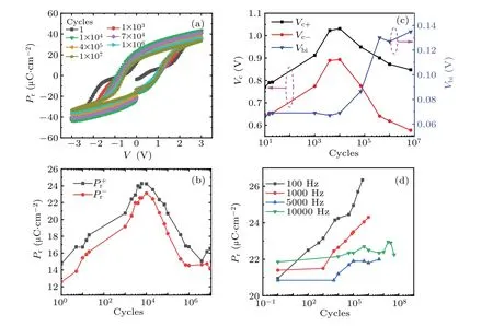
Fig. 1. Changes in (a) P–V hysteresis loops, (b) remnant polarization, (c) coercive voltage and built-in voltage with switching cycles under 1-kHz square waves. (d)Changes in remnant polarization as a function of switching cycles under square waves with various frequencies.
The wake-up test was also performed under various frequencies, as shown in Fig. 1(d). As the switching frequency decreased, fewer switching cycles were needed to reach the same polarization increase relative to that from higher switching frequencies. This was consistent with previous results that a higher number of cycles was necessary to acquire the same remnant polarization at higher wake-up frequencies.[13]
The dominant conduction mechanism for the HZO thin film was analyzed. It was firstly polarized with +3 V to preset the polarization state. Then theI–Vcurve was measured in the 0→3 V region, as illustrated in Fig. 2(a) with a double-logarithmic scale. As the voltage increased, theI–Vcurve exhibited a linear behavior (slopekof 1.1) at low voltage(<0.6 V),and then a quadratic behavior(k=2.2)at higher voltage.At 1.7 V,the current rose sharply and the slope was 6.9. The conduction behavior was consistent with trapcontrolled space-charge-limited(SCL)conduction,[22–24]with three regions corresponding to Ohmic, SCL, and trap-filledlimited conduction.[25]The origin of the space charges in the ferroelectric material is related to oxygen vacancies.They create trap energy levels in the bandgap for activated electrons to be mobile.[22]Thus, it is reasonable to assign oxygen vacancies as the physical origins for the traps in the film.Figure 2(b)displays theI–Vcurves for various numbers of switching cycles. It reveals that both the linear part (Ohmic conduction)and the SCL current remained stable up to 105cycles,indicating that the number of charge carriers associated with oxygen vacancies did not change in the wake-up process. This was consistent with previous results that no oxygen vacancies were generated in the wake-up stage.[12]
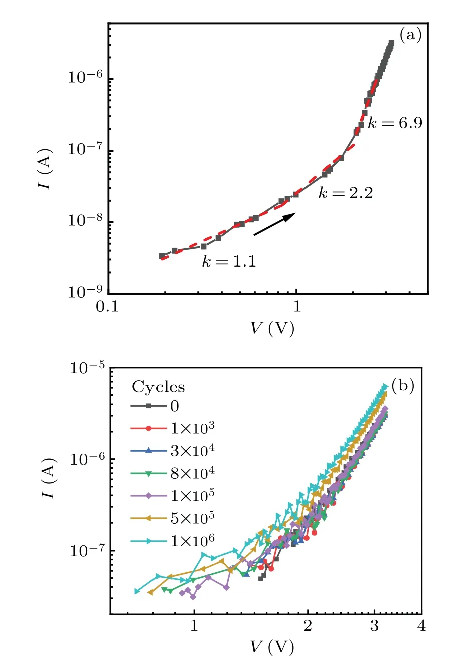
Fig. 2. (a) The I–V characteristics under positive bias. The arrow denotes the sweep direction. (b) Changes in I–V curves with respect to switching cycles.
The device was also repetitively switched with 1-kHz,±3 V pulsed waveforms. The pulse width ranged over 0.01–0.5 ms.It can be seen from Fig.3(a)that when the pulse width was less than 0.1 ms,the polarization did not exhibit a wakeup effect. Only when the pulse width was a certain length did the wake-up appear, which implied that the voltage application time in each switching cycle was an important factor. We plotted the remnant polarization over the total duration of the applied field for both square and pulsed waves in Fig. 3(b).The longer voltage application times in each cycle resulted in a faster wake-up. Furthermore,a wake-up also occurred when a DC voltage was applied. In Fig.3(b),the rise of remnant polarization under continuous DC voltage was close to that from the cycling wake-up for the equivalent duration. Hence, we can explain the wake-up effect in terms of the redistribution of oxygen vacancies,although there is no generation of new V¨Oat this stage. The positively charged oxygen vacancies moved under the external electric field. When the application time of each voltage cycle did not reach a certain limit,the vacancies just vibrated in their original positions and did not change their distribution. When the application time was sufficiently long,the V¨Oleft their initial positions, resulting in a net migration and redistribution that contributed to the wake-up process. In that case, both the voltage application time in each cycle and the cumulative electric field duration affected the wake-up process.
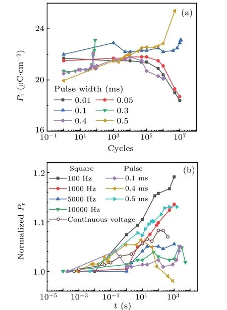
Fig. 3. (a) Change in remnant polarization as a function of switching cycles under 1-kHz waves with various pulse widths. (b) Normalized change in Pr over the duration of the switching electrical field for both square (#cycles/frequency) and pulse waveforms (#cycles×pulse width×2). The results are compared with the rise of Pr under a continuous DC electric field.
For further verification,C–Vloops were measured for the cycled samples. In Fig. 4(a), the capacitance decreased with the increasing number of electric field cycles. Lomenzoet al.[26,27]suggested that the decreased dielectric constant in the wake-up state was caused by the tetragonal-to-ferroelectric orthorhombic phase transition. Pintilieet al. proposed that theC–Vcurve of a ferroelectric material can be expressed by[17,28]
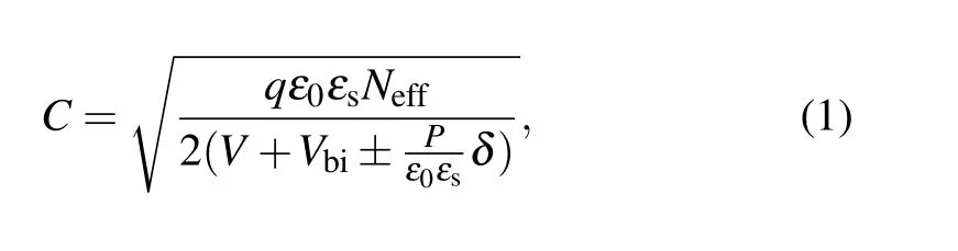
whereNeffis the effective charge density in the space-charge region of the Schottky diode,Vbiis the built-in potential in the absence of polarization,δis the distance between the polarization sheet of charge and the physical metal–ferroelectric interface,qis the carrier charge,ε0is the permittivity of free space, andεsis the static dielectric constant. The±sign indicates two possible orientations of polarizationP. TheC–Vcurve in the area enclosed by the green dashed line in Fig.4(a)was chosen and the corresponding slope of 1/C2–Vwas fit to extractNefffor the interface under reverse bias. The inset in Fig.4(b)displays the linear fit of such a relationship to derive the initial charge density near the top electrode/film interface.The dependence ofNeffon switching cycles is illustrated in Fig.4(b)for the top and bottom interfaces.
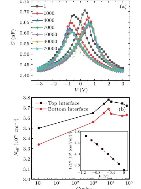
Fig.4.(a)Change inC–V characteristics for the HZO thin film with various switching cycles. (b)Change in free-carrier concentration at both top and bottom electrode/film interfaces with respect to the switching cycles. The inset shows the 1/C2–V plot of the initial sample.
It shows that the effective charge density at the interfaces increased during wake-up. This could also be understood in terms of oxygen vacancy migration which is shown in Figs. 5(a)–5(c). Because the V¨Owith positive charges can attract electrons, they usually act as electron-trapping centers.[17]Initially, the V¨Oaccumulated at the TiN/HZO interface (Fig. 5(a)), where a large number of electrons were needed to fill traps, causing a small density of free charge in the space-charge region. As the wake-up process continued during the initial 104cycles,the oxygen vacancies moved away from the interface and went into the bulk of the HZO film as shown in Fig. 5(b), reducing the amount of V¨Oat the interface. Therefore, the charged-carrier trapping was reduced,which resulted in an increased effective charge density at the interfacial space-charge region. It can also be derived that there should be a higher concentration of V¨Oat the bottom interface than that at the top interface from the comparison ofNeffbetween the two interface as shown in Fig.4(b).This gave rise to an upward built-in voltage[29]consistent with the result shown in Fig.1(c). After the wake-up stage, the film was fatigued to have an obvious reduction in polarization. On the basis of the long-term study of fatigue mechanism,the fatigue behavior is considered to be closely related to the generation of oxygen vacancies in the film.[30,31]The increase of oxygen vacancies caused the reduction of effective charge density after 104cycles as shown in Fig.4(b). It is possible that the difference between the concentration of V¨Oat the top and bottom interface became larger (Fig. 5(c)). As a result, the built-in voltage increased rapidly in the fatigue process as displayed in Fig. 1(c). However, the scenario requires for more investigation in future work.
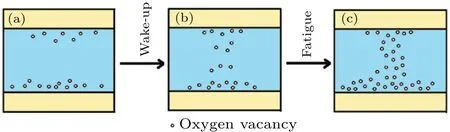
Fig.5. Schematic of the migration and generation of oxygen vacancies from(a)initial →(b)wake-up →(c)fatigue state under the repetitive switching process. The hollow circles represent the oxygen vacancies.
4. Conclusions
The wake-up effect in the TiN/Hf0.4Zr0.6O2/TiN structure was examined with various electrical cycling conditions. The total duration and the single length of an applied electrical field both affected the increased polarization. The current–voltage characteristics were consistent with space-charge-limited conduction. Both the stable Ohmic and SCL currents in the wakeup process indicated that the trap density in the film did not change during this period. The effective density of charge in the space-charge region demonstrated a decreased trap density at the interface. Considering the important role of oxygen vacancies as trap centers and their migration under an electric field, the wake-up effect and other property changes were attributed to the redistribution of oxygen vacancies.
Acknowledgements
Project supported by the National Natural Science Foundation of China (Grant No. 61201046) and the Natural Science Foundation of Beijing, China (Grant Nos. 4202009 and 4162013).
猜你喜欢
Plasma Science and Technology(2022年5期)2022-06-01
科教新报(2022年17期)2022-05-24
Plasma Science and Technology(2021年6期)2021-06-21
Plasma Science and Technology(2021年6期)2021-06-21
Plasma Science and Technology(2020年3期)2020-04-24
书法赏评(2019年2期)2019-07-02
北京文学(2018年9期)2018-09-13
美与时代·美术学刊(2018年2期)2018-04-12
民间故事选刊·上(2015年8期)2015-09-10
微型小说选刊(2014年14期)2014-05-17

- Chinese Physics B的其它文章
- Direct measurement of two-qubit phononic entangled states via optomechanical interactions
- Inertial focusing and rotating characteristics of elliptical and rectangular particle pairs in channel flow
- Achieving ultracold Bose–Fermi mixture of 87Rb and 40K with dual dark magnetic-optical-trap
- New experimental measurement of natSe(n,γ)cross section between 1 eV to 1 keV at the CSNS Back-n facility
- Oscillation properties of matter–wave bright solitons in harmonic potentials
- Synchronously scrambled diffuse image encryption method based on a new cosine chaotic map