
Photon-interactions with perovskite oxides
2022-08-31 09:55HongbaoYao姚洪宝ErJiaGuo郭尔佳ChenGe葛琛CanWang王灿
Chinese Physics B 2022年8期
关键词:王灿
Hongbao Yao(姚洪宝) Er-Jia Guo(郭尔佳) Chen Ge(葛琛) Can Wang(王灿)
Guozhen Yang(杨国桢)1,2, and Kuijuan Jin(金奎娟)1,2,3,†
1Beijing National Laboratory for Condensed Matter Physics,Institute of Physics,Chinese Academy of Sciences,Beijing 100190,China
2University of Chinese Academy of Sciences,Beijing 100049,China
3Songshan Lake Materials Laboratory,Dongguan 523808,China
Keywords: laser molecular-beam epitaxy,optical second harmonic generation,functional oxides
1. Introduction
The interactions of photon and condensed material systems involve a variety of physical processes and result in diverse effects.[1–4]Among correlated material systems, intensive attention has been paid to the perovskite oxides due to their ferroelectricity, ferromagnetism, and optical nonlinearity arising from the strong couplings among charge, lattice,orbital,and spin degrees of freedom.[5–8]In this paper,we focus on the following three effects of the interactions between laser and perovskite oxides: the ionization and nucleation in laser molecular-beam epitaxy (laser-MBE), the nonlinear responses in the second harmonic generation(SHG)technique,and the photoelectronic effect in oxides.With the development of modern smart devices, the size of computing unit shrinks significantly and the integration level enhances dramatically,thus the interfaces between different perovskite oxides gradually play a dominant role in the performance and functionalities of devices composed of those materials.[9–12]“The interface is the device,”Nobel laureate Herbert Kroemer famously claimed, refers to the remarkable ground-breaking properties to be found at the heterojunctions where layers of different materials meet.[13,14]Emergent phenomena at the interfaces between perovskite oxides, such as two-dimensional electron gas,[15,16]the interfacial superconductivity,[17–19]magnetoresistance(MR),[20,21]resistive switching,[22–24]and interfacial ferroic orderings,[25–27]have been discovered. These interfacial properties generate increasing interests for developing high-density, fast-response, and low-power-consumption device units.[23,28]The precise fabrication of atomically flat oxide interfaces is highly required not only in fundamental research, but also in the high-quality functional devices.Over decades, scientists found that the interfacial coupling effects, such as charge transfer, strain engineering, and spin reconstruction, decay severely with the increase of the layer thickness,[29]leading to the deterioration of interfacial modulations and device performance. Therefore, developing the detection methods to the interfacial structure and physical properties, especially the noninvasive detection means, is of great significance to understand the dynamic process of intercoupling mechanism and further to maximize their intriguing functionalities.
Over past decades, a variety of deposition schemes have been invented for the fabrication of desired low-dimensional thin films and heterostructures.[30]Molecular-beam epitaxy(MBE) has exhibited complete capabilities to nearly perfect crystalline quality,flat surface,and abrupt interfaces.[30]However, the MBE became overwhelmed in facing of complex perovskite oxides, which intrinsically manifest high melting point (∼2000◦C) and complex chemical compositions. To eke out from this disadvantage,researchers replaced the heating coils in MBE with the intense laser to evaporate the source materials, and thus developed the so-called laser-MBE.[31]By this technique, researchers have been granted the controllability over single atom of perovskite oxides, and have realized even monolayer-by-monolayer alternation of oxide materials.[32]The advances in synthesis of perovskite oxides,in turn, improve the functionalities of these materials. In the nondestructive detection of surface, interfaces, and interiors of perovskite oxide structures,the optical SHG technique has shown unique advantage over other means for its high sensitivity to the space-inversion symmetry breaking and the interactions among domains of perovskite oxides.[33–35]Utilizing SHG,the symmetry breaking at surface and interface,the polar state, the evolution of structure with strain or temperature, as well as the weak couplings among ferroelectric nanodomains, of perovskite oxides have been successfully unveiled. In this review, we firstly report the recent progress in the high-precision synthesis and functional optimization of low-dimensional perovskite oxide structures using laser-MBE assisted by excimer high-energy photons.The second part will highlight the applications of the SHG technique in the detection of surface/interface symmetry breaking, polar state, domain distribution,and weak couplings among nanoscale ferroelectric domains,of non-centrosymmetric perovskite oxides.
2. Laser molecular-beam epitaxy
The maximization of the functionalities originating from interfacial modulations requires the thin films with impeccable quality,atomically-flat surface,and precise thickness even down to the monolayer limit. Practically, there are three nucleation modes during the deposition of thin films: the Frank–van der Merwe(layer-by-layer)mode,the Volmer–Weber(island) mode, and the Stranski–Krastanov (layer-plus-island)mode. The Frank–van der Merwe (Volmer–Weber) mode occurs when the surface energy of the substrate surfaceγsis larger (smaller) than the sum of that of the filmγfand that of the interface between the substrate and the filmγsf.The Stranski–Krastanov mode initializes with layer-by-layer growth mode and alters to subsequent island growth mode when triggered by other energy contributions (e.g., strain energy).
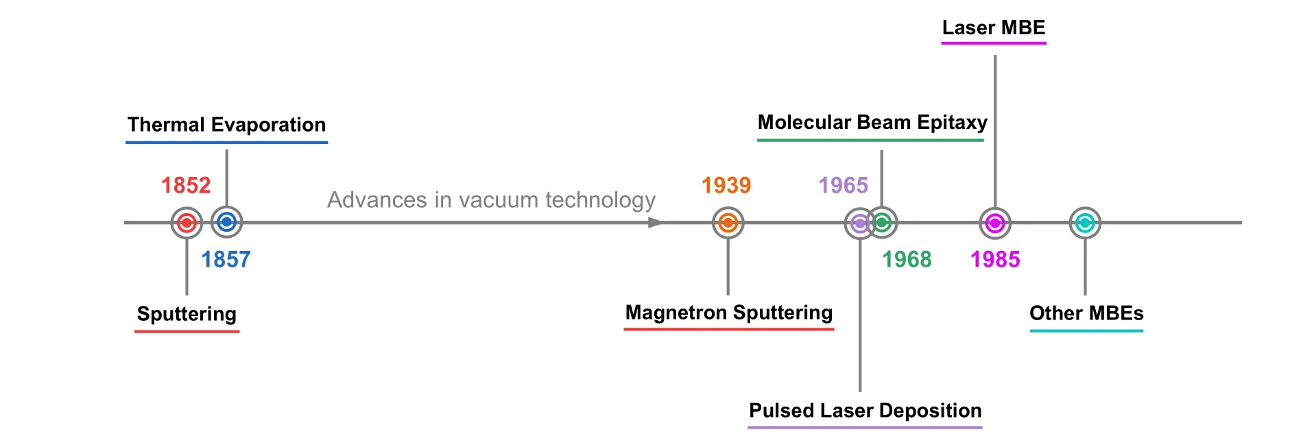
Fig.1. Timeline of the introduction of physical vapor deposition techniques.[30] Figure was reproduced from Ref.[30]with permission.
High-quality low-dimensional materials with exotic phenomena and maximized functionalities put stringent demands on the manufacturing techniques to possess a layer-by-layer integration mode, ideal controllability over the single atomic layer, and that over oxygen contents. In the past decades,a lot of vapor deposition methods have been invented for the synthesis of ideal low-dimensional condensed matter systems,[30]such as sputtering,[36]thermal evaporation,[37]magnetron sputtering,[38]atomic layer deposition,[39]pulsed laser deposition,[40]and MBE[41](Fig. 1). Among those methods, the MBE has been barged to the forefront since its first application at 1970s. As the MBE is a kinetic process, that is, the incident neutral particles are stacked one by one on the substrate for growth, rather than a thermodynamic process, so it is capable of growing thin films that are difficult for ordinary thermal equilibrium methods.[41]With MBE, researchers have even realized the synthesis of a series of one-unit-cell-thick monatomic (silicene, germanene,stanene, hafnene, borophene, phosphorene, bismuthene, and antimonene)and diatomic(hexagonal boron nitride,transition metal dichalcogenides, copper selenide, silver telluride, and FeSe) semiconductors and superconductors up to now.[42,43]However,the MBE falls short when coming to complex oxides with high melting point.In order to evaporate these source materials, researchers brought intense laser into MBE, and thus developed laser-MBE.[31]The laser pulse with nanosecond and hundred mJ energy is irradiated onto the ceramic target surface and excites the ionized plasma out of the targets. The plasma is sputtered onto the heated single crystal substrates,as shown in Fig.2(a),[44]and the sample can be subsequently harvested in the form of thin films,[45–51]heterostructures,[52–55]and superlattices.[56–59]Meanwhile,in order to identify theinsitugrowth process of low-dimensional structures,a variety of monitoring techniques have been elaborately developed,such as the oblique incidence reflectance difference,[60]surface photo-absorption,[61]spectral ellipsometry,[62]p-polarized reflectance spectroscopy,[63]and reflection high-energy electron diffraction (RHEED).[64]Among these advanced techniques,the RHEED outcompetes for its high sensitivity to variations of the surface topography andin-situmonitoring of the inplane crystalline structure simultaneously. The high-energy electron beam in RHEED glancingly incidents on the substrate at a small angle of 1◦–3◦and reflects to a fluorescent screen (Fig. 2(b)).[65]The intensity of the reflective electron beam changes accordingly with the roughness of substrates.Each intensity oscillation corresponds to the growth of an atomic layer. By counting the RHEED oscillations,we could monitor the layer-by-layer growth of thin films, as shown in Fig.2(c).[65]Using this method, the laser-MBE is able to accomplish unit-cell-by-unit-cell growth and real-time monitoring of the film thickness and their crystal structure. Specially,the laser-MBE is an ideal means to fabricate the high melting point,complex composition,and multiple elements materials,such as perovskite oxides. We will discuss the advantages of oxide thin film deposition using laser-MBE in the following sections.
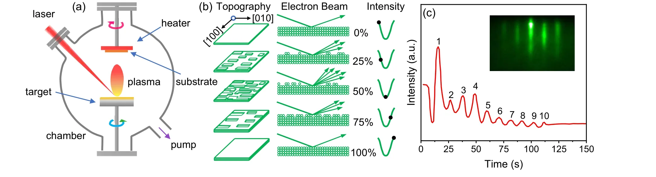
Fig.2.(a)Illustration of a laser-MBE system.[44](b)Surface morphology and diffraction intensity during the deposition of a single atomic layer.[64](c)Recorded RHEED oscillations during the deposition of La0.8Sr0.2MnO3 thin film. The inset shows the RHEED pattern of the film.[65] Figure was reproduced from Ref.[64]with permission.
2.1. Atomically precision structural engineering by laser-MBE
The state-of-the-art workmanship exploiting the laser-MBE in multifunctional perovskite oxides is the epitaxy of ultra-thick single-crystalline films[66,67]and the precision synthesis of monolayer-thick films with atomically abrupt surface and interface.[32]In 2001, G. Z. Yanget al.[66]had realized the homoepitaxy of a SrTiO3layer with a thickness more than 1000 u.c. on the(001)-oriented SrTiO3substrates. Figure 3(a)shows partial real-time RHEED oscillations during the film growth.[66]Atomic force microscopy and high-resolution scanning transmission electron microscopy(STEM)results revealed that the surface of the sub-micrometer thick SrTiO3film still maintained atomically smooth.[66]Such atomic-scale controlled epitaxy of oxide films can be used for constructing artificially designed oxides that exhibit unexpected physical properties and emergent phenomena,and therefore opens a door for investigating the underlying physical mechanisms and stimulates the potential applications based on oxides.[66]Except for the ultra-thick epitaxy, the single-unit-cell precision growth of perovskite oxides is also a world-class challenge,which requires the fine control of lots of growth parameters andin-situmonitoring of the layer growth extremely carefully.Figure 3(b) shows a STEM image of a single-unit-cell thick LaCoO3layer embedded in a matrix of SrCuO2layers.[23]The clear “dark stripes” in the superlattices represent the atomically thin LaCoO3, which exhibits different out-of-plane lattice constants compared to those of the SrCuO2layers. The atomic-precision-controlled growth can maintain up to 15 bilayer’s repeats with abrupt interfaces and uniform layer thickness.
Aside from the epitaxy of single layer of perovskite oxides, the laser-MBE technique has also made great progresses in creating new functionalities by stacking different perovskite oxides together. In order to examine the nature and length scales of charge screening in complex oxides, A. Ohtomoet al.[29]have fabricated an idealized heterostructure with one-unit-cell interlayer of LaTiO3embedded in SrTiO3layers. Despite the chemical abruptness of the interfaces, they found that a minimum thickness of five atomic buffer layers was required for the center titanium site to recover bulk-like insulating properties by fully screening the electronic gas generated at the LaTiO3/SrTiO3interfaces.Their work represented a framework within which the shortlength scale electronic response can be incorporated in thin film oxide heterostructures.[29]Moreover, by making the utmost of laser-MBE capability, S. Liet al.[32]succeeded in fabricating a superlattice composed of one-unit-cell-by-oneunit-cell alternation of LaCoO3and SrCuO2layers(Fig.3(c)).They achieved a surprisingly strong ferromagnetism in atomically thin cobaltite by local structural modification. The magnetic moment and Curie temperature of one-unit-cell LaCoO3layer were larger than those previously reported for any monolayer oxides. Thus, the strategy for creating functional quantum heterostructures by exploiting atomic interfacial engineering provides great opportunities for discovering novel interfacial physics and stimulating potential applications in the quantum heterostructure.[32]
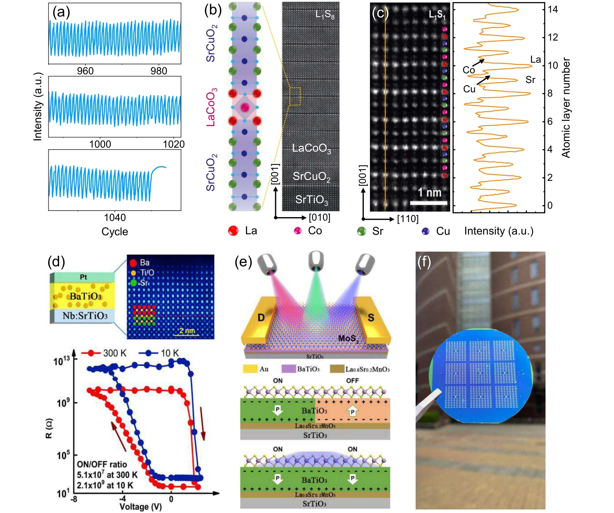
Fig.3. (a)The 950–1050th RHEED oscillations during the homoepitaxy of SrTiO3 on SrTiO3.[66] (b)STEM image and schematic of single-unit-cell precision controlled LaCoO3 layer embedded in 8-u.c.-thick SrCuO2 layers.[32] (c)STEM image and intensity profile of a superlattice with alternative single-unit-cell thick LaCoO3 and SrCuO2 layers.[32](d)Illustration of(upper)Pt/BaTiO3/Nb:SrTiO3 heterostructure and(lower)its resistance–voltage curve at different temperatures.[68](e)Schematic illustration of(upper)optoelectronic synapses stimulated by three types of light pulses and(lower)the photo-induced polarization switching in the BaTiO3 film underneath the monolayer MoS2.[69] (f)Photograph of the neuromorphic sensor array.[70,71]Panels(a),(b)–(c),and(e)were reproduced from Refs.[66],[32],and[69],respectively,with permission.
2.2. Maximizing the functionality of perovskite oxides by laser-MBE
Simultaneously, with the advances of laser-MBE technique,the functionalities of perovskite oxide heterostructures have been greatly improved. Taking ferromagnetic perovskite oxides as an example, numerous efforts have been devoted to the enhancement of the MR magnitude. Typically, MR is evaluated by (RH −R0)/R0, where theR0andRHrepresent the resistances under the magnetic fields of 0 andH, respectively. In the past decades, the giant negative MR down to four orders of magnitude reduction in resistivity had been achieved in manganite thin films.[21]Previously,the giant MR was obtained at relatively low temperatures(e.g.,60 K)under large magnetic fields (e.g., 80000 Oe). The extreme conditions limit the real device applications based on MR effect.K.J.Jinet al.[20]reported a distinct positive colossal magnetoresistance at the interfaces between p-type La0.9Sr0.1MnO3and n-type SrNb0.01Ti0.99O3near the room temperature. Surprisingly,the positive magnetoresistance can be even achieved with a tiny magnetic field of only 5 Oe.[20,72]The intriguing phenomenon and its underlying physics not only stimulate the further theoretical work, but also imply the potential applications of magnetic sensors and nonvolatile data storage devices with ultrahigh sensitivity and extremely low power consumption.Recently,with the improvement of laser-MBE technique,the long-range room-temperature ferromagnetic ordering has even been achieved at the interfaces of the antiferromagnetic oxides and the antiferromagnetic nitrides.[73]This finding not only opens new avenues for potential applications, but also provides an access to hidden phases at low-dimensional quantum heterostructures.[73]
In the research area of ferroelectric perovskite oxides,the key parameters (ON/OFF ratio) of ferroelectric tunneling junctions (FTJs) regarding to their future applications in the nonvolatile memory devices and neuromorphic computing devices have been greatly improved in recent years.[74–76]In 2017, C. Yoonet al.[9]fabricated a FTJ composed of Ag,PbZr0.52Ti0.48O3,and La0.8Sr0.2MnO3,and reached a recordhigh ON/OFF ratio up to 107. Meanwhile,the Ag ion migration in this ultrathin FTJ has enabled an ultralow energy consumption (potentiation energy consumption∼22 aJ and depression energy consumption∼2.5 pJ).Following this work,J. K. Liet al.[68]have achieved a giant ON/OFF ratio of 5.1×10⁷at room temperature and 2.1×10⁹at 10 K in a Pt/BaTiO3/Nb:SrTiO3FTJ (Fig. 3(d)), which functionalizes with ON and OFF states depending on the polarization direction of the BaTiO3layer. This result pioneers the design of high-performance resistive switching devices based on ultrathin oxide heterostructures using electric field controlled ionic engineering.[68]Exploiting the ON/OFF ratio, recently,J.Y.Duet al.[69]have successfully developed high-efficiency MoS2/BaTiO3optoelectronic synapses(Fig.3(e)). These neuromorphic vision sensors work on the multiple resistance states resulting from the photo-induced ferroelectric polarization reversal of the BaTiO3layer (Fig. 3(e)). Furthermore,based on the multiple resistance states of vanadium dioxides with the stimulation of light, G. Liet al.[70]have developed the optoelectronic neuromorphic sensors with both the high sensitivity for ultraviolet light and the nonvolatile multi-level storage characteristics. Benefitting from the simulations of these oxides prepared by laser-MBE to optoelectronic neuromorphic units, the artificial neural networks consisting of these optoelectronic sensors (Fig. 3(f)) are able to perform neuromorphic computing and image preprocessing, and significantly promote the image recognition accuracy from 24%to 93%.[70,71]These optoelectronic devices integrating sensing, memory, and processing functions can be integrated on silicon at the wafer-scale,and have greatly improved the efficiency of artificial vision systems,and offered new opportunities for near-sensor and in-sensor computing.[70,71]
The multifunctional perovskite oxides grown by laser-MBE have also demonstrated significantly improved performance in the high-density energy storage.[77]In 2021,H. Panet al.[78]reported a serial of dielectric supercapacitors with ultrahigh energy preservations. Specifically, the Sm-doped 0.3BiFeO3–0.7BaTiO3(Sm-BFBT) relaxor ferroelectrics exhibited an energy storage density of 152 J/cm3, a world record in the same type of oxide materials. This work demonstrates a generic approach to dielectric energy storages with high energy density and continuously improved efficiency by compositional control and polymorphic domain design through laser-MBE.Besides,a series of oxide films fabricated by laser-MBE are able to manifest better superconducting functionalities. For example, in the nickelate oxide films synthesized by laser-MBE technique,scientists have achieved a pressure-induced monotonic enhancement of critical temperature(Tc)to over 30 K in the superconducting Pr0.82Sr0.18NiO2thin films,[79,80]which is the highestTcamong nickelates so far.[79,80]
3. Optical second harmonic generation
Interface between different oxides plays a dominant role in their physical properties. Suitable detection methods on the surficial and interfacial structures and properties are highly demanded in both fundamental understandings and practical applications. Photon detections have unique advantages over other physical detection means. First of all, it is nondestructive and non-contact means. The sample quality and surface/interface largely preserve its virgin states after the measurements. Secondly, the optical detection is fast. Both static and dynamic processes of interfacial properties can be probed in a short time-frame, sometimes even in the femtoseconds. It allows us to investigate the ultrafast responses in the structural variations or magnetoelectric properties. Lastly, the photons with different energy and wavelength have high penetration depth. The structural changes buried under deep interfaces can be probed and this hidden information normally is important for the throughout understanding of their interfacial properties. By exploiting the interactions of photon and multifunctional perovskite oxides, serval techniques, such as the Raman spectra,[81]fluorescence spectrum, ultrafast optics,[82]and optical SHG,[83]have been developed for the nondestructive access of physical properties of multifunctional perovskite oxides. Among these different investigation methods, the SHG technique has outperformed for its splendid sensitivity and resolution to the symmetry and interactions among domains of perovskite oxides.[5,33,34,84]As the simplest nonlinear optical response,SHG is the process that a focused fundamental light (with frequency ofω)irradiates on the sample and emits a doubled frequency light (with frequency of 2ω).[85]Typical configurations of SHG scheme with far-field reflection and transmission modes are illustrated in Figs.4(a)and 4(b),respectively.The intensity of the SH componentI2ωat the fixed incident laser powerIωcan be described as
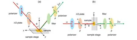
Fig.4. Illustration of far-field(a)reflective and(b)transmission SHG system.
By detecting the optical signals, SHG can be used to study the symmetry of non-centrosymmetric structures,[87]which manifest the removal of an inversion center due to the macroscopic discontinuities or microscopic symmetry breaking,[88–90]such as the sample surface,[83,91,92]the interfaces within heterostructures and superlattices,[93–96]and the intrinsic ferroelectrics.[97,98]In past decades, extensive attention has been paid to the symmetry determinations of surface and interfaces in perovskite oxide films using SHG where the SH polarimetry directly reflects the symmetry,and its intensity dominates the strength of the polarization within those structures. It has also been successfully applied to determine the polar state, domain distribution, and interactions among individual domains within many functional oxide films. Below we summarize several examples in which the SHG technique plays a determinative role in their functionalities.
3.1. Determining the surface/interface symmetry using SHG
The surface and interfaces in the complex oxide heterostructures exhibit the natural symmetry breaking due to the discontinuity of different materials. It contributes to the intrinsic nonlinear optical signals. Therefore, the SH components from the surface and interfaces can be accurately identified prior to complex structures of perovskite oxides.R. Q. Zhaoet al.[35]revealed that the surface of (100)-orientated cubic SrTiO3and(111)-orientated cubic Nb:SrTiO3substrates present an equivalent 4mmand 3mpoint group,respectively. By implanting an underneath buffer layer, the intensity of SH response of SrTiO3surface can be significantly enhanced through the interfacial effects.[35]Recently,H.Zhaoet al.[99]reported the emergence of the SH signals in AB-type superlattices where A and B represent centrosymmetric SrTiO3and LaTiO3, respectively. In these lattices, there are no macroscopic broken inversion symmetry, and thus the SH responses were assumed generated by the SrTiO3/LaTiO3interfaces.[99]They proposed that such interfaces composed of centrosymmetric layers demonstrated an equivalent 4mmsymmetry,in consistent with that of the(001)SrTiO3surface(which can be regarded as an interface between the SrTiO3and air/vacuum) revealed in previous work.[35]Furthermore, the SH polarimetry could be tuned in these superlattices by tailoring the number of SrTiO3/LaTiO3interfaces.These two examples provide inspirations for isolating the SH signals of material interiors from those of surface and interfaces in perovskite oxide structures with surface/interfaces exhibiting equivalent symmetry of4mmpoint group, in which the SH signal at the normal incidence scheme will only contain the SH response from the material bulk.
3.2. Quantifying the polar states using SHG
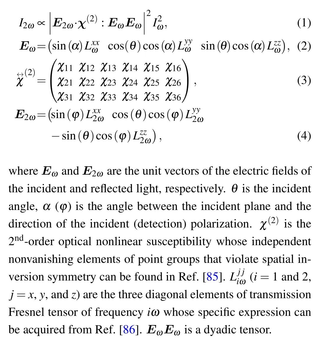
For the intrinsic ferroelectric materials possessing a remnant polarization,SHG is one of the most powerful techniques to analyze their polar states.[100]Because the SHG only probes the polar distortions projected on the plane perpendicular to the incident light,[101–103]it is, therefore, accessible to disentangle the SH component of in-plane orienteda-domains and out-of-plane pointedc-domains by changing the orientation of the polar axis with respect to the incident light.[100]Uniaxial tetragonal ferroelectric PbZr0.2Ti0.8O3shows a thicknessdependent domain distribution upon its complex domain variations.[104]A fully strained PbZr0.2Ti0.8O3thin film possesses the singlec-domain state(Fig.5(a)),whereas a relaxed thick PbZr0.2Ti0.8O3film presents a coexistence ofa- andcdomains.[105,106]Thec-oriented PbZr0.2Ti0.8O3whose polar axis is parallel to thec-axis exhibits no SH response at normal incidence(θ=0◦). If the incident beam tilts away from thecaxis,the SH signal increases with the tilting angle(Fig.5(b)).It is caused by the increasement of the projected polarization on the plane orthogonal to the incident light. As shown in Fig.5(c), the angular dependence of SH response(at an incident angle of 40◦)identifies the projection of the polar distortion to be along the direction of the double-lobe shape.[100]For the thick PbZr0.2Ti0.8O3films withc-domains and nanosized stripea-domains (Fig. 5(d)), the normal incidence configuration allows the discrimination of the in-plane (black) contributions from the out-of-plane (red) contributions to the nonlinear optical responses[107](Fig. 5(e)). Specifically, at the normal incidence, the SHG intensity associated with the outof-plane domains vanishes,but that from the in-plane domains remains. For instance, figure 5(f) shows the SHG results of a PbZr0.2Ti0.8O3thick film with normal incidence. The results clearly highlight the presence of a macroscopic in-plane polarization.[100]
In the presence of complex domain architectures where two sets of orthogonally orienteda-domains coexist,[106]the SH signals will not yield the spontaneous polarization of each domain. Instead,they reflect the direction of the macroscopic in-plane net polarization coming from the sum of alla-domain contributions.[100]Therefore,the correspondence between the angular dependence of the SH response and the orientation of the polar axis can be exploited further to identify the direction of a net polarization when more complex domain structures are considered. For example, the domain-engineered multiferroic BiFeO3films subjected to an in-plane anisotropic strain present two ferroelectric variants arranged in a stripe pattern[5](Fig. 6(a)). The in-plane projections of the polarization in adjacent domains differ by 90◦, as highlighted by the small white arrows in the piezoelectric force microscopy(PFM) scan (Fig. 6(a)). This difference produces an average net in-plane polarization orthogonal to the domain wall elongation,as indicated by the large white arrow in Fig.6(a).In the case of normal incidence (Fig. 6(b)), the angular dependence of the SH signal manifests as a two-fold symmetry oriented along the macroscopic net polar axis direction,[5]as shown in Fig. 6(c). In the absence of such in-plane polarization anisotropy(Fig.6(d))and in case of normal incidence(Fig. 6(e)), four equivalent ferroelectric variants nucleate.[5]These results are confirmed by the absence of an average macroscopic in-plane polarization(Fig.6(f)).
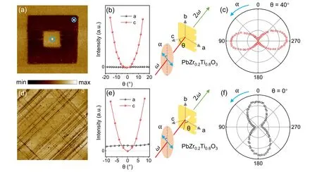
Fig. 5. (a) Piezoelectric force microscopy of PbZr0.2Ti0.8O3 thin film with out-of-plane polarization only.[100] (b) Second harmonic intensity on the angle θ between the incident light beam and a axis,and on that angle between the incident light beam and c axis.[107] The schematic diagram denotes the illustration of incidence. (c)SH polarimetry pattern at an incidence angle of 40◦.[100] (d)–(f)Corresponding result of PbZr0.2Ti0.8O3 thin film with coexisting in-plane and out-of-plane polarization to(a)–(c),respectively.[100,107]The incidence angle in(f)is 0◦.Panels(b),(d),and(e)were reproduced from Ref.[107]with permission.
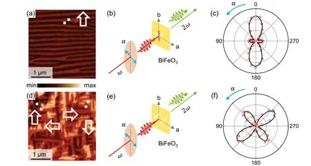
Fig. 6. (a) PFM of BiFeO3 thin film with two in-plane domains.[5] The two small arrows indicate the polarization direction of these two domains,and the big one denotes the net polarization. (b)Illustration of incidence. (c)Corresponding SH polarimetry to(b).[5] (d)–(f)Corresponding results of BiFeO3 thin film with random in-plane domains to(a)–(c),respectively.[5] Panels(a),(c),(d),and(f)were reproduced from Ref.[5]with permission.
Fig. 7. SH polarimetry patterns of BiFeO3 films of (a) T- and (b) R-like phase.[5] (c) SH intensity dependence on the angle θ between the incident light beam and c axis for BiFeO3 films of(red)T-and(green)R-like phase.[111] (d)–(f)SH polarimetry patterns of BiFeO3 films of 4 nm,100 nm,and 180 nm,respectively,grown on Nb:SrTiO3 substrate.[86]Panels(a)–(b)and(c)were reproduced from Refs.[5]and[111],respectively,with permission.
Furthermore,SHG is also capable of detecting subtle polar changes, such as strain-induced monoclinic distortions, in the epitaxial perovskite oxide films. In particular,the BiFeO3films will present a tetragonal-like(T-phase)crystalline structure under extremely large compressive strain.[108]As the compressive strain relaxes,BiFeO3film will maintain its bulk rhombohedral-like(R-phase)structure.[109]These two phases possess the same monoclinic point group(m),and the only difference between those two phases is that the R-phase BiFeO3rotates relatively its in-plane polarization by 45◦at the unitcell level.[110]To distinguish this subtle change in the crystal structure is a challenging task for many techniques. However,SHG methods can separate these two phases firmly by observing the direction of the double-sided lobes,[5]as shown in Figs.7(a)and 7(b).The R-and T-phases can also coexist in the same thin film. The SHG contributions associated with these two phases have different relative intensities as a function of the incident angle[111](Fig. 7(c)). The T-phase (red) has a symmetric behavior similar to a genuine tetragonal structure,
whereas the SH response of the R-phase (green) reflects its polarization anisotropy. These distinct behaviors allow associating the nonlinear optical output at different incident angles to the two ferroelectric phases.[111]Another effective way to investigate the strain effects on the epitaxial films is to compare the films with variable thicknesses on a substrate. The strain will relax with increasing film thickness, and this strain evolution results in a symmetry change between T-and R-phases in BiFeO3films with increasing film thickness. The ultrathin BiFeO3film (4 nm) grown on a Nb:SrTiO3substrate suffers from a compressive strain.[86]A four-fold rotational symmetry associated with the absence of in-plane anisotropy is subject to the T-phase BiFeO3,[86]as shown in Fig.7(d). As the film thickness increases to∼100 nm,both T-and R-phases present in a BiFeO3single thin film[86](Fig.7(e)). The SH signal exhibits a clear transition from four-fold to two-fold rotational symmetry. We could also identify that the polar axis of the R-phase is fully developed in a 180-nm-thick BiFeO3film,[86]as shown in Fig. 7(f). Therefore, the sensitivity of the SHG method allows us to precisely determine the subtle changes in the crystalline symmetry, even though the two variants are extremely close to each other.
3.3. Determining the domain distribution by SHG
Spatial arrangement of the same polar axis (state) identifies the single-polarized domain of ferroelectrics. Therefore, spatial scanning of the SH response is able to unveil the domain distribution of ferroelectrics. By switching the polarization of multiferroic BiFeO3films using in-plane PFM, J. Y. Chauleauet al.[112]created an area with fullya-oriented polarization. The polar axis is indicated by an arrow in Fig. 8(a). The SH intensity of this switched domain exhibits evident distinction to those of the as-grown one under SHG mapping, even at the normal incidence (Fig. 8(b)).Meanwhile, the uniform contrast inside this engineered domain further announces that the intensity of the polarization is approximately identical within this switched area. Aside from the domain originating from the ferroelectric polarization, SHG mapping is also capable of unmasking the ordering arising from antiferromagnetism (Fig. 8(c)).[112]In structures with simultaneous non-vanishing ferroelectric and magnetic orders, the SHG tensorχ(2)can be described asχ(2)=χ(f)+χ(m),whereχ(f)andχ(m)correspond to the tensor component associated with crystallographic(ferroelectric)and magnetic orders, respectively.[112]The SH signals from ferroelectric and magnetic orders usually manifest different dependences on the polarization of the incident light,and this difference results in small asymmetry in the SHG patterns of the structures with both non-zero ferroelectric and magnetic SHG tensors. Therefore,the best fitting of experimental SHG patterns by the combination of ferroelectric and magnetic SH contributions allows us to separate the SH signals from ferroelectric polarization and magnetic structures. In engineered domain with uniform in-plane polarization in Fig.8(a),the polarimetry of the SH response has shown three different patterns,[112]as shown in Figs. 8(d)–8(f), respectively.Two domain patterns present small asymmetry in the SHG signals (Figs. 8(d) and 8(e)). They believed that the subtle changes in the symmetry may come from the antiferromagnetic ordering in the films. Quantitative disentanglement of the total SH signal revealed the spatial distribution of antiferromagnetic ordering hidden below the ferroelectric ordering(Fig.8(c)). Moreover,the SHG mapping has been competent to distinguish the antiferromagnetic ordering outside the domain engineered area,as indicated by ellipses in Figs.8(b)and 8(c),where lacks a net ferroelectric polarization.Additionally,assessed by SHG, the ferroelectric and antiferromagnetic domains can behave independently, i.e., the ferroelectric (antiferromagnetic) switching does not necessarily generate evolution in the antiferromagnetic (ferroelectric) ordering, thus revealing that magneto-electric coupling can lead to various arrangements of the two orders.[112]Beyond the new insight provided on the intimate nature of magneto-electric coupling at the microscopic scale,this property permits one to envisage a two-level coding where classical ferroelectric information can be complemented by a built-in discrete antiferromagnetic message.[112]This work apparently strongly depends on the sensitivity of signals from distinct domains using SHG mapping technique. The clear visualization allows scientists to independently control ferroelectric and antiferromagnetic writing using external fields.
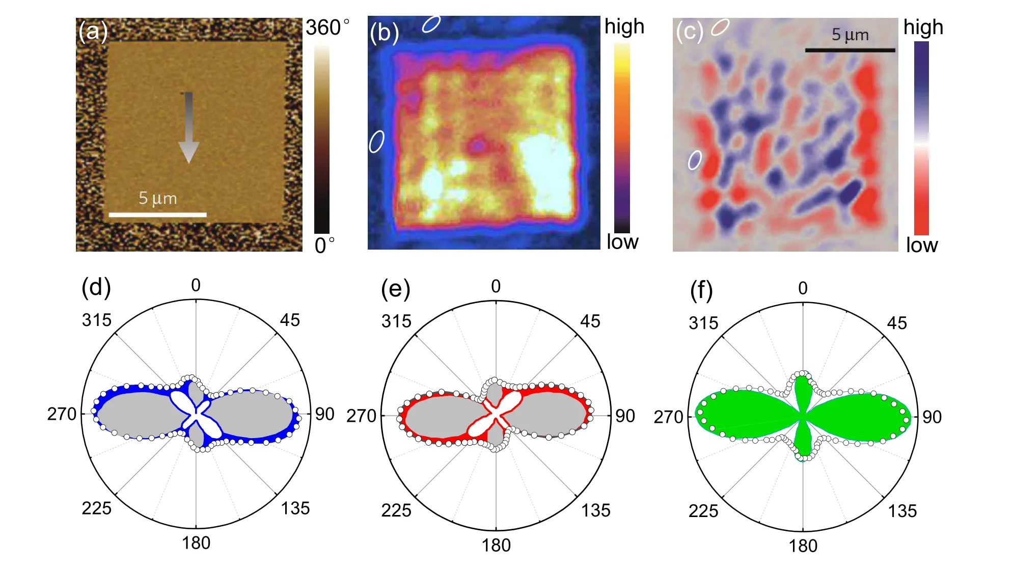
Fig.8. (a)PFM of BiFeO3 thin film with engineered in-plane domain,the polarization direction of which is indicated by the arrow.[112](b)SH response of areas in(a).[112] (c)The antiferromagnetic ordering hidden inside the ferroelectric domain.[112] (d)–(f)Three distinct SH polarimetry patterns within the switched domain in(a).[112] The opened dots are the experimental data. The blue,red,and green filled areas are the fits of the SH data,composed of the ferroelectric part(grey areas)and the antiferromagnetic part(white areas). Figure was replotted from Ref.[112]with permission.
3.4. Weak ferroelectric coupling illustrated by SHG

Fig.9. (a)–(b)STEM of Sm-BFBT films with Sm doping of x=0 and 0.3, respectively.[78] Green dashed lines delineate domain areas, in which red arrows denote the orientation of net polarization. (c)–(d)Phase diagram and SH intensity dependence on temperature of Sm-BFBT films with different doping,respectively.[78] The black lines around Tm in(d)indicate the change of the dependence of SH intensity on temperature for all Sm-BFBT films.(e)SH polarimetry of Sm-BFBT film with Sm doping of x=0.3 at different temperatures.[78] Figure was reproduced from Ref.[78]with permission and reanalyzed by the authors. We added SHG results of x=0.15 in(d)in addition to the published results in Ref.[78].
When scaling down to nanometer, the domains of ferroelectrics degenerate into polar nanoregions, i.e., local symmetry broken. The PFM and other scanning probe techniques have been successfully applied in the observation of polar state and domain distribution in the multifunctional perovskite oxides. However, they fell short when coming to the characterizations of weak ferroelectric couplings among nanoscale domains. In these systems with nanodomains, e.g., relaxor ferroelectrics[113]and molecular ferroelectrics,[114]the SHG technique has great advantage over the other means. Through varying doping concentration(x),H.Panet al.[78]elaborately modulated the domain size of relaxor ferroelectric Sm-BFBT films into nanoscale, as indicated in Figs. 9(a) and 9(b). In these films, the polymorphic nanodomain designs have opened a window for the emergence of the super-paraelectric state,which were purposed by Cross[113]for relax ferroelectrics and were featured with weak couplings among nanodomains. Despite massive explorative studies, only circumstantial evidences for its existence were reported.[77]Here, by utilizing temperature-dependent SHG technique,which announces thein-situevolution of the interactions among ferroelectric domains,we have directly proven the existence of such super-paraelectric phase in the engineered nanocrystalline film of Sm-BFBT.Moreover, we have also determined the specific temperature range of that phase in these films[78](Fig. 9(c)). Specifically, with increasing temperature, the SH intensities from the relaxor ferroelectric regime are weaker than those from the ferroelectric phase in all Sm-BFBT films (Fig. 9(d)).[78]This decrease of SH response indicates the vanishing of the long-range ferroelectric order and the weakening of interactions among the ferroelectric domains. This weak coupling can be distinguished by optical methods. In the superparaelectric regime, the SH intensities further reduce, and reach the minimal values with only residual surface signals at their respective Burns temperature (TB), above which the coupling of nanodomains vanishes. The persistence of SH intensities in the temperature segment between the temperature corresponding to the maximum dielectric constant of Sm-BFBT (Tm) andTBindicates the presence of polar domain structures. This result provides solid evidence on the theoretically predicted super-paraelectric state in these materials. Figure 9(e)shows the SH polarimetry measured at representative temperatures in the relaxor ferroelectric,super-paraelectric,and paraelectric segments for Sm-BFBT film(x=0.3).[78]The film exhibits weaker intensity but similar SH polarimetry in the super-paraelectric segment relative to those of the relaxor ferroelectric state. Hence,although a decline of interactions among domains in Sm-BFBT occured during the state transition from relaxor ferroelectric to superparaelectric, the crystal structure of these films still remained tetragonal. In the state transition from super-paraelectric to paraelectric, however, the structural symmetry of Sm-BFBT transformed from tetragonal to cubic,with point group altering from 4mmtom¯3m.[115]Additionally, the intensity anomalies near 450 K were ascribed to thermally enhanced local disorders in the nanodomain structures,originating from the order–disorder phase transition of the BaTiO3component in these films.[115–117]These results indubitably evince the capability of SHG technique in the unveiling of the subtle evolutions in perovskite oxides.
As one can tell from above examples, the SHG technique has achieved significant success in the probe of surface/interface symmetry,polar state,domain distribution,and weak couplings among nanodomains of multifunctional perovskite oxides. The accurate interpretations of the measured SH signals from complex structures, however, still remain challenging. In most ferroelectrics,the SH contributions from the surface and interfaces can be ignored because their intensities are much smaller than those from the interiors of the ferroelectrics. In these systems with weak couplings, however,the SH signals from the surface and interfaces become comparable with those from ferroelectrics interiors,and cannot be ignored. Although the SH components from some surface and interfaces have been clarified,the precise deconvolution of SH signals has not been well presented due to the intimate entanglements among the SH response from the sample surface,interfaces,and interiors.
4. Conclusion and perspectives
In summary, regarding the interactions of photon and multifunctional perovskite oxides, we summarized the applications in the thin film fabrication and intriguing property detection using laser-MBE and optical SHG technique, respectively. We discussed the atomically precision structural engineering of perovskite oxide thin films and heterostructures.Then,we enumerated the potential applications based on their functionalities,e.g.,giant ON/OFF ratio,ultralow energy consumption, and ultrahigh energy storage. With the development of laser-MBE technique, the low-dimensional quantum heterostructures with emergent phenomena were discovered.The proof-of-principle devices with evolutionary performance are expected and will prominently promote the great advances in the material sciences and information technologies. Along with the development of SHG technique, we narrated the recent progresses in the determination of surface/interface symmetry, polar state, domain distribution, and weak couplings among nanodomains of the functional perovskite oxides. Notably,although the optical SHG has achieved immense accomplishments in these materials, the disentanglement of nonlinear optical responses from the surface, interfaces, and interiors in complex structures has not been well understood. To bring the external stimulus, such as the temperature, magnetic/electric fields, microwaves, and mechanical stress, into the SHG detection surely will introduce the advantages in understanding the coupling between lattice and other degrees of freedoms in the transition metal oxides and other quantum materials.Also,scientists are eager to detect the nonlinear optical responses from a segment in nanoscale. The outcomings will not only extend the length scale of research targets, but also help to obtain the underlying mechanism that has never been explored using traditional detection methods.
Acknowledgments
Project supported by the National Key Basic Research Program of China (Grant Nos. 2017YFA0303604,2019YFA0308500,and 2020YFA0309100),the National Natural Science Foundation of China (Grant Nos. 11721404,11934019, 11974390, and 12074416), the Youth Innovation Promotion Association of the Chinese Academy of Sciences(Grant No. 2018008), the Beijing Nova Program of Science and Technology (Grant No. Z191100001119112), Beijing Natural Science Foundation (Grant No. 2202060), and the Strategic Priority Research Program (B) of the Chinese Academy of Sciences(Grant No.XDB33030200).
猜你喜欢
财会月刊·上半月(2022年5期)2022-05-17
中华环境(2022年3期)2022-03-31
新作文·小学低年级版(2018年12期)2018-11-29
作文新天地(高中版)(2017年1期)2017-03-13
民生周刊(2011年1期)2011-04-20
法律与生活(2009年5期)2009-04-10

- Chinese Physics B的其它文章
- Direct measurement of two-qubit phononic entangled states via optomechanical interactions
- Inertial focusing and rotating characteristics of elliptical and rectangular particle pairs in channel flow
- Achieving ultracold Bose–Fermi mixture of 87Rb and 40K with dual dark magnetic-optical-trap
- New experimental measurement of natSe(n,γ)cross section between 1 eV to 1 keV at the CSNS Back-n facility
- Oscillation properties of matter–wave bright solitons in harmonic potentials
- Synchronously scrambled diffuse image encryption method based on a new cosine chaotic map