
Multiplexing technology based on SQUID for readout of superconducting transition-edge sensor arrays
2022-10-26 09:47XinyuWu吴歆宇QingYu余晴YongchengHe何永成JiansheLiu刘建设andWeiChen陈炜
Chinese Physics B 2022年10期
Xinyu Wu(吴歆宇), Qing Yu(余晴), Yongcheng He(何永成),Jianshe Liu(刘建设), and Wei Chen(陈炜)
School of Integrated Circuits,Tsinghua University,Beijing 100084,China
Keywords: superconducting transition-edge sensor arrays, superconducting quantum interference devices,multiplexing technology,cryogenic readout
1. Introduction
Superconducting transition-edge sensors (TESs) are highly sensitive for incident energy or power at cryogenic temperatures. Since TESs are applicable to a broad wavelength range, cryogenic detectors based on TESs have a wide range of applications. TES microcalorimeters can achieve excellent energy resolution when detecting high-energy photons such as x rays and gamma rays.[1–5]TES bolometers are widely used in cosmic microwave background(CMB)experiments due to low noise level and good response linearity.[6–10]TES single photon detectors have high detection efficiency and photonnumber-resolving capability,which can meet the measurement requirements in the field of quantum optics.[11–15]These applications drive the development of large-scale TES arrays to further improve collection efficiency,counting rate and sensitivity of TESs.Superconducting quantum interference devices(SQUIDs) are one of the most sensitive sensors of magnetic flux, which are typically used as amplifiers to detect physical quantities that can be converted into magnetic flux.[16]Because the SQUID amplifier has low input impedance, low noise and low power dissipation,it is preferred for the readout of the TES detector.[17,18]
However,as the number of TES detectors in the array increases, the complexity of wiring and the thermal load pose great challenges to the cryogenic readout. Therefore, it is essential to employ SQUID-based multiplexing technologies in which multiple TES detectors share one readout line. The scale of TES arrays largely depends on the number of TES detectors per readout line,which is referred to as the multiplexing factor. To increase the scale of TES arrays and to boost the performance of readout circuits, different multiplexing schemes have been proposed and developed. Currently,these schemes include time-division multiplexing (TDM), codedivision multiplexing (CDM), frequency-division multiplexing(FDM)and microwave SQUID multiplexing(MW-Mux).No matter which scheme is employed,the first step is to limit the bandwidth of all TES signals to avoid aliasing of out-ofband noise into the signal bandwidth.[19,20]After bandwidth limitation,TES signals from different channels are combined into a small number of readout lines and transmitted to roomtemperature electronics for demodulation and identification.In order to achieve the accurate measurement and the scalable readout of TES signals,these multiplexing schemes focus on improving circuit architectures, electronical components,control algorithms and room temperature hardware. As for applications of various spectrometers and astronomical telescopes,emerging readout systems need to measure thousands of TES detectors while maintaining low readout noise and low crosstalk.
Despite great advances in SQUID-based multiplexing technologies, they still need to be optimized. As the scale of TES arrays continues to extend, the design requirements for multiplexing technologies increase, which mainly focus on the multiplexing factor, readout noise, channel-to-channel crosstalk and operational complexity. Due to parameter constraints in readout circuits,it is difficult for each technology to satisfy the requirements simultaneously. From the perspective of practical applications,the choice of multiplexing technologies is generally a trade-off among these design requirements.In view of this, this paper summarizes the different types of SQUID-based multiplexing technologies and discusses their parameter constraints. The sections are organized as follows:Section 2 briefly introduces the readout circuit of the TES and the orthogonal modulation functions used in different multiplexing technologies. Sections 3–6 describe circuit architectures and parameter constraints of each technology. Section 7 compares characteristics of these multiplexing technologies.Section 8 gives a summary and outlook.
2. Readout circuit of TES
The superconducting transition-edge sensor is essentially a thermistor.[21,22]The measurement of TES signals is of success by measuring the change of TES resistance induced by the energy of incident photons. Figure 1 shows the schematic of the readout circuit of a single TES.In the TES bias circuit,the TES resistanceRTESis in parallel with a bias resistorRbiasand in series with an input coilLinand a Nyquist coilLNyq. The bias resistor with resistance being much smaller than the TES resistance is used to realize the voltage bias of the TES. The voltage-biased TES operates at the electro-thermal negative feedback(ETF),exhibiting fast response and low noise.[23,24]The Nyquist coil is used to construct anL/Rlow-pass filter in the TES bias circuit, where the inductanceLindicates the total inductance of the input coil and the Nyquist coil,and the resistanceRindicates the total resistance of the bias resistor and the TES.ThisL/Rlow-pass filter can effectively limit the bandwidth of the TES signal, avoiding the aliasing of highfrequency noise. The current flowing through the TES is inductively coupled to a SQUID (SQ), generating a flux in the SQUID loop. The voltage across the SQUID varies according to the flux-voltage characteristics of the SQUID.Then,the output voltage of the SQUID is transmitted from the cryogenic stage to the room-temperature preamplifier. The role of the SQUID is providing the necessary transimpedance gain for the TES current to suppress the noise of preamplifier. In order to keep the output of SQUID in a small linear regime, the readout circuit employs a flux-locked loop(FLL)[25]in which the feedback current is inductively coupled to the SQUID through a feedback resistorRfb.
The TES coupled to the SQUID has been proven to show excellent single-pixel performance. However,for TES arrays,it is difficult to have a readout line for each pixel because each readout line brings a thermal load to the measurement system.In this case, SQUID-based multiplexing technologies, which can dramatically reduce the number of readout lines,are necessary for the readout of large-scale TES arrays.
In SQUID-based multiplexing technologies,different orthogonal modulation functions are used to encode and decode the TES signals.[26–28]In TDM,the functions areNlow-dutycycle square waves. In CDM, the functions correspond to anN-dimensional Walsh matrix in whichNmust be a power of two. In FDM,the functions correspond toNsinusoids which modulate TES signals to different frequencies. The functions of MW-Mux are similar to that of FDM.Therefore,the significant difference among these multiplexing technologies is the schemes used to combine and distinguish TES signals from different channels. These schemes are divided into time domain and frequency domain. In the following, this paper details these multiplexing schemes in the sequence of TDM,CDM,FDM and MW-Mux.
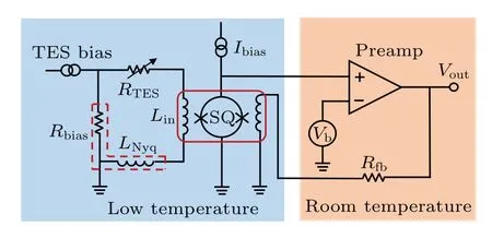
Fig. 1. Schematic of the readout circuit of a single TES. The SQUID chip(red solid box) generally consists of a SQUID amplifier, an input coil and a feedback coil. The Nyquist chip (red dotted box) generally consists of a bias resistor and a Nyquist coil.
3. Time-division multiplexing
At present, TDM is well-established for the readout of TES arrays. In the TDM circuit, each TES is equipped with a SQUID amplifier, which together constitute a pixel. In an individual column, TDM turns on each row of SQUIDs sequentially and combines the signals from different pixels into a common readout line.
3.1. TDM circuit architecture based on flux summing
The mature version of TDM circuits is based on an architecture which utilizes an approach of flux summing.[29]Figure 2 shows the schematic of this version. In each unit pixel,the TES is inductively coupled to a first-stage SQUID amplifier(SQ1). All the TESs operate in voltage-biased mode and remain active all the time. The SQ1 of each row is turned on by applying the row-address current (Iad) to the corresponding row-address line. Then, the current signal from SQ1 at a time is passed to a common second-stage SQUID (SQ2)via an intermediate summing coil. Next, the current signal from SQ2 is amplified by a third-stage SQUID array which is connected to room-temperature electronics. The entire TDM circuit uses a flux-locked loop (FLL) to keep the output signal of SQUID arrays within a small linear range. Each column in the circuit shares a feedback line through which a proportional-integral feedback signal(Vfb)is inductively coupled to SQ1s. The FLL is either traditional analog integrator circuits[30]or digital feedback control circuits(DFB).[31,32]This version of TDM circuits has been fielded in a variety of x-ray spectrometers.[33–35]The circuit architecture in Fig.2 is a three-stage SQUID configuration. Actually,the architecture can be either two-stage or three-stage,as long as the configuration provides sufficient power gain for TES signals.
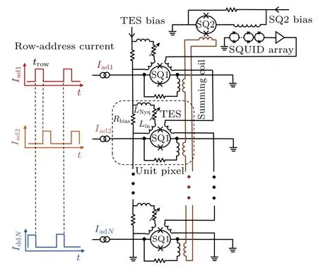
Fig.2. Schematic of an N-row TDM circuit. The figure is taken from Ref.[29].
3.2. TDM circuit architecture based on superconducting switch
The TDM circuit above has a complex layout,and its row switching rate is not high enough. After iterative upgrades,TDM circuits have evolved into some new versions.[36–38]Compared with TDM circuits based on the flux summing,these versions remove the intermediate summing coil and introduce additional superconducting switches actuated by magnetic flux. Figure 3 shows the schematic of anN-row TDM circuit based on the flux-actuated superconducting switch. In each unit pixel, the superconducting switch (marked by a red dotted box) is in parallel with an input SQUID (SQ1 or SQ2···SQN)and an addressing resistorRadd. The addressing resistor is used to dissipate the weak loop current and its resistance needs to be smaller than the SQUID dynamic resistance to reduce its voltage noise. These superconducting switches are shorted in the non-address state. When a row-address current is applied to one switch,the switch is turned on while the others in the column are left shorted. In this situation,the signal from one SQUID is measured only once in one cycle of the row-address current. Compared with TDM circuits based on the flux summing,TDM circuits based on the superconducting switch have faster row switching rate and lower readout noise.
One form of the superconducting switch is the Zappestyle interferometer.[39]It includes tow-junction, threejunction and even multiple-junction configurations. In these configurations, Josephson junctions are connected in parallel by superconducting inductors and the feed point of the bias current is flexible. The bias current of the Zappe-style interferometer is set to be smaller than the critical current of the Josephson junction. Under this condition, the interferometer is in the zero-voltage state and the load of the interferometer is effectively shorted. When the critical current is reduced below the bias current by the external control current, nearly all the junction current flows into the load. The threshold curve of the Zappe-style interferometer can be adjusted by the critical current of the Josephson junction,the inductance and the feed point of the bias current,making the Zappe-style interferometer adaptable to different applications.

Fig.3. Schematic of a TDM circuit with flux-actuated superconducting switches. The figure is taken from Ref.[36].
Another form of the superconducting switch is the SQUID-based switch.[36]The switch is essentially a SQUID with the extremely small loop inductance. In this SQUID,the screening parameter (βL≪1) is so small that the critical current of the SQUID approaches to zero at half-integer flux quanta. Similarly,the hysteresis parameterβCneeds to be sufficiently small to ensure that the current-voltage characteristics of this SQUID is non-hysteresis.The operation of the SQUIDbased superconducting switch is as follows. The bias current(Ibias) of the entire loop is selected to be not only slightly larger than the current(Isq)used to bias the input SQUID,but also smaller than the critical current(Ic)of the SQUID-based switch at integer flux quanta.When the flux through the switch is of integer flux quanta, the switch is in the superconducting state and the input SQUID is shorted. When a current that generates a flux of half-integer flux quanta is applied to the row-address line, the switch is in the resistive state and most ofIbiasflows into the input SQUID.As long as circuit parameters are designed properly,the current flowing into the input SQUID can be equal toIsqused to activate the input SQUID.The SQUID-based switch is generally in the form of a SQUID series array(SSA)to minimize loading of the activated input SQUID. The input SQUID can be either a single one or an array. An array configuration is preferable because it can improve the noise impedance match between SQUIDs and room temperature electronics.[40–42]
In the TDM circuit with superconducting switches discussed above, the number of row-address lines (used to turn on rows of SQUIDs)increases with the increase of the multiplexing factor,adding the burden of wiring. In order to alleviate the burden, an advanced two-level switch is proposed.[43]Figure 4 shows a simple example of the two-level switch.Nsuperconducting switches are divided intoN1groups(the first level),and each group containsN2switches(the second level),i.e.,N=N1×N2. In this new architecture,the number of rowaddress lines reduces fromN1×N2toN1+N2.This advantage becomes significant when the scale of TES arrays expands.However,extending the switches to multi-level structure complicates the design of cryogenic chips and room-temperature electronics.
因此,本研究旨在探究GDM产妇产后血糖复查的阻碍与促进因素,为制定完善有效的干预措施提供参考。现报告如下。
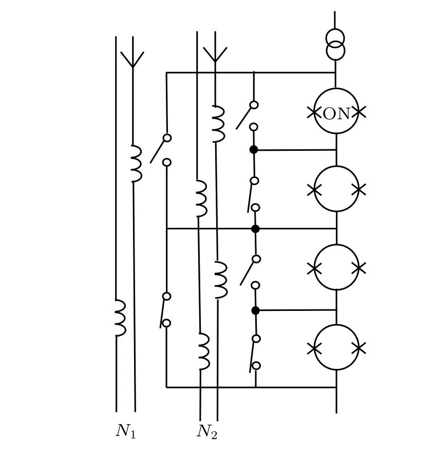
Fig. 4. The simple two-level switch layout. The figure is taken from Ref.[43].
3.3. Parameter constraints in TDM
In practical applications, TDM has its own parameter constraints. On the one hand, TDM imposes strict requirements on the sampling frequency. When rows of a TDM circuit are turned on sequentially,the row time which dwells on a row is denoted asδtrow. For anN-row TDM circuit,the frame rate at which all the pixels in each column are measured can be expressed asfframe=1/(Nδtrow). According to the Nyquist–Shannon theorem,the frame rate needs to satisfy the following condition to prevent high-frequency noise from aliasing into the signal bandwidth:
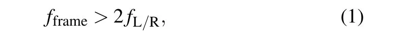
wherefL/Ris the cut-off frequency of the L/R low-pass filter in the TES bias circuit. The inductanceLis the sum of the input inductance, the Nyquist inductance and the stray inductance.The resistanceRis the total resistance in the TES bias circuit.Meanwhile, the TES under electrothermal negative feedback(ETF)should satisfy the following condition[44]to ensure the stability of the device:
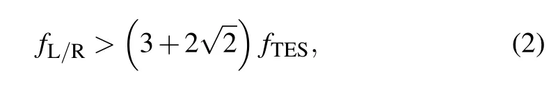
wherefTESis the thermal response frequency of the TES.The sampling frequencyfsample, which denotes as the switching rate between adjacent rows, isNtimes the frame rate. Combining the conditions above,the sampling frequency is limited to the following condition:

It can be seen that TDM requires an extremely high sampling frequency when it is used to read out fast photon signals or a large number of pixels. In addition, when the TDM circuit switches from one row to the next,SQUIDs require a settling time to establish a stable state due to the transient response of the electronic components.[45]As a result,the time that can be used to sample is even shorter than the row time, presenting an additional challenge to the sampling frequency. Although an extra inductor in series with TES can limit the signal bandwidth and thus reduce the settling time,it comes at the expense of the reduction of signal-to-noise ratio(SNR).


4. Code-division multiplexing

4.1. Flux-summation architecture
Φ-CDM achieves different coupling polarities between the signal and the SQUID by changing the direction of the input coil in the TES bias circuit.[50]Figure 5 shows a schematic of a four-rowΦ-CDM circuit which is based on a three-stage SQUID architecture. In theΦ-CDM circuit,the polarity combination of each row used to encode TES signals corresponds to the Walsh function. As with TDM, each row of theΦCDM circuit is turned on by applying row-address currents in sequence. TES signals with different polarity combinations are coupled to the first-stage SQUIDs (SQ1). Next, the signals from different rows are passed to a common SQUID amplifier (SQ2) through an inductive coil. The signals from SQ2 are amplified by a SQUID array and transmitted to roomtemperature electronics for demodulation. The original TES signals can be demodulated and identified according to the inversion of Walsh matrix. When any SQUID in the circuit is taken for observation, all the TESs are connected to this SQUID.The SQUID noise in CDM can be improved because the SQUID in each row observes the Walsh-coded TES signals simultaneously.Φ-CDM is developed straightly based on TDM and shares similar low-pass filters with it.
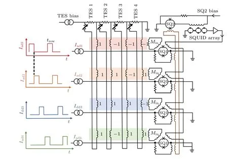
Fig.5. Schematic of a four-row Φ-CDM.The figure is taken from Ref.[50].
4.2. Current-steering architecture
InI-CDM, the polarity switching of TES signals is realized through a single-pole double-throw(SPDT)switch.[51]Figure 6 shows the schematic of a four-rowI-CDM circuit and an SPDT switch integrated with a TES bias circuit. The SPDT switch consists of two SQUID-based switches connected in parallel. Each branch contains a SQUID-based switch (actually a DC-SQUID with the extremely small loop inductance),a series resistorRser,and an inductive coil coupled to the summing coil. The coupling polarity between one branch and the summing coil is positive (mutual inductance +M) while the other is negative(mutual inductance-M). The critical current of the DC-SQUID with the extremely small loop inductance approaches zero at half-integer flux quanta. In the implementation ofI-CDM, a flux offset ofΦ0/2 is applied to one of the SQUID-based switches in the SPDT to make the critical current of that switch reduce to a minimum. In this case,one SQUID-based switch becomes resistive state (RN) while the other keeps superconducting state.Since the normal resistance of the SQUID-based switch is much larger than the series resistance, i.e.,RN≫Rser, almost all of the TES current flows through the superconducting SQUID-based switch. The coupling polarity between the TES signal and the summing coil can be adjusted by applying row-address currents to generate 0 orΦ0/2 flux in the entire SPDT switch. The row-address currents inI-CDM correspond to the Walsh matrix. The difference between row-address currents inΦ-CDM andI-CDM is that currents inΦ-CDM are applied sequentially to rows in a cycle while currents inI-CDM are simultaneously applied to rows.

Fig.6. Schematic of a four-row I-CDM circuit and an SPDT switch integrated with a TES bias circuit. The figure is taken from Ref.[51].
4.3. Parameter constraints in CDM
Both CDM approaches also have some constraints in common. Firstly, the coupling polarity in the first channel of CDM is always positive,which easily induces large crosstalk from feedback signals of other channels.[51]In practical applications, the first channel is usually used to characterize common coherent noise sources and the rest are used to read out TES detectors.Secondly,CDM is vulnerable to the signal loss.Since each SQUID in a column is a necessary component to obtain the encoded TES signal, a failed SQUID can result in the loss of an entire column of TES signals.To solve this problem, an error correction (EC) which replaces one TES with a constant signal is used to recover TES signals in the case of a failed SQUID.[52]A configurable error correction integrated with a cryotron switch in the TES bias circuit is also demonstrated.[53]In room-temperature electronics of CDM,a complex set of algorithm software is required to perform the Walsh encoding. Meanwhile,the channel crosstalk caused by parallel readout needs to be optimized.[54]

5. Frequency-division multiplexing
FDM combines and distinguishes signals from different channels in the frequency domain,which is an attractive technology for the readout of TES arrays and has some different characteristics.
5.1. FDM circuit architecture
In the implementation of FDM at MHz frequencies, the TES detector is ac-biased.[60,61]Figure 7 shows the schematic of anN-channel FDM circuit. In each unit pixel,the TES resistanceRTESis connected with an inductorLand a capacitorCto form an LCR filter on the sub-Kelvin stage. The TES resistance and the inductor in all channels are the same while the capacitor is different from each other. In each channel,the bandwidth for the TES detector is expressed asR/2πLand the resonant frequency of the LCR filter is determined by the value of the capacitance. Bias carriers with different frequencies are applied to TES bias circuits and thus TES signals are modulated to high frequencies. The LCR filter of each channel is used to pass through the target carrier frequency and suppress out-of-band signals and noise. When the TES resistanceRTESchanges, the corresponding carrier is amplitude modulated and the TES signal is encoded in sidebands above and below the carrier. These encoded TES signals from different channels are coupled to a common SQUID amplifier(typically a SQUID array) on the Kelvin stage. Then output signals of the SQUID are passed to room-temperature electronics for demodulation.

Fig. 7. Schematic of an N-channel FDM circuit. The figure is taken from Ref.[61].
Since signals from individual channels are coupled to a common SQUID amplifier, the dynamic range of the SQUID that can accommodate the carrier signals is limited.In order to extend the dynamic range of the SQUID,a carrier comb with a phase shift ofπ,which is referred to as the nulling comb,is injected at the input of the SQUID to cancel the carrier signals applied to TESs.[62]Another effective way to this problem is feedback. Some studies have shown that baseband feedback(BBFB)[63]or digital active nulling(DAN)[64]can increase the dynamic range of the SQUID, allowing an increased number of TES detectors per readout SQUID.The complexity of code for BBFB is comparable to the code for frame-delayed flux feedback used in TDM, which is important for practical applications of FDM.The improvement to the dynamic range of the SQUID can also be reached by increasing the number of SQUIDs for readout within a dissipation budget constraint.
5.2. Parameter constraints in FDM
However,FDM has its own problems. Firstly, compared with the dc-biased TES in TDM and CDM,the ac-biased TES in FDM shows resolution degradation.[66,67]Secondly,the size of filter elements in FDM is slightly larger than that in TDM and CDM. The inductor in FDM is effectively same as the Nyquist inductor in TDM or CDM, and the capacitor in the optimally dimensioned circuit is approximately the same size as the inductor.[68]In an optimal case, the size of filter elements of FDM is twice that of TDM or CDM.[69]Thirdly,the crosstalk effect in FDM circuits makes it difficult to accurately demodulate carriers and identify TES signals in roomtemperature electronics. It has been suggested that one of the reasons for the crosstalk effect is due to the nonlinearity of the SQUID response.[70]Some other contributions to channel-to-channel crosstalk include the coupling between inductors of different channels, bias carrier leakage and nonzero SQUID/wiring impedance.[71]In order to prevent channel crosstalk, the frequency space between adjacent resonances needs to be sufficiently separated.[72,73]

6. Microwave SQUID multiplexing
Another technology for reading out signals in the frequency domain is MW-Mux. Because MW-Mux can provide hundreds of MHz or even several GHz bandwidths for the whole readout circuit, it attracts extensive attention in recent years.
6.1. MW-Mux circuit architecture
MW-Mux retains the key attribute of dc-biased TES detectors as with TDM and CDM.Figure 8 shows the schematic of a microwave SQUID multiplexing circuit. In the MW-Mux circuit, each TES is coupled to an intermediate SQUID. The SQUID can be either a DC-SQUID[77]or a dissipationless RF-SQUID.[78–80]Each SQUID is coupled to a high-Qmicrowave resonator which has a unique resonant frequency.The TES current is inductively coupled to the SQUID and generates a flux in the SQUID. The change of the flux results in a change in the Josephson inductance of the SQUID,causing a shift in the resonant frequency of the corresponding resonator. The microwave SQUID multiplexer contains many resonators which are all coupled to a common coplanar waveguide(CPW)readout line. The frequency shifts induced by TES signals are probed by applying a comb of microwave signals to the CPW readout line.[81]The probed signals are amplified by a high-electron-mobility transistor(HEMT)amplifier at 4 K and then passed to room-temperature electronics for demodulation.

Fig.8. Schematic of a three-pixel microwave SQUID multiplexing circuit. The figure is taken from Ref.[81].
6.2. Flux ramp modulation
Since the flux-voltage characteristics of the SQUID is periodic, the feedback loop is required to keep the response of the SQUID in a linear range and to bias the flux at a sensitive point of the SQUID response curve. Typically, TDM,CDM and FDM are all configured with feedback loops. Nevertheless,the flux-locked loop seems not to be compatible with MW-Mux. An alternative approach for MW-Mux is flux ramp modulation.[82]When a periodic sawtooth-shaped current signal is applied to a common modulation coil and generates a linearly rising flux ramp of an integer flux quanta in the SQUID, the SQUID response changes according to its fluxvoltage characteristics. The flux ramp repetition rateframpcorresponds to the effective sampling frequency of TES signals. Whenframpis larger than the slew rate of the input signal, the phase shift of the flux-voltage characteristics is a linear function of the amplitude of the input signal. A change of one flux quantum corresponds to a phase shift of 2π. The phase shift can be determined by using software-defined radio(SDR)-based readout electronics.[83]
Flux ramp modulation can not only provide a linear measurement for the input signal,but also increase the usable dynamic range of the SQUID.In practical applications,different types of TES detectors have different requirements onframpand the bandwidth of the resonator is adjusted according toframp. The bandwidth of the resonator can be set by adjusting the strength of the capacitive coupling between the resonator and the CPW readout line.
6.3. Parameter constraints in MW-Mux
The significant advantage of MW-Mux is the large readout bandwidth. The large readout bandwidth enables MWMux to measure a large number of TES detectors simultaneously. Alternatively, MW-Mux can allocate sufficient bandwidth for each pixel,which is suitable for the readout of TES detectors with rapid signal rate and high bandwidth requirements. In practical applications of MW-Mux, the number of TES detectors in each readout channel (the multiplexing factor) is limited by the allowable resonance spacing and the available bandwidth of room-temperature electronics.
Firstly, the sufficient resonance spacing in MW-Mux is required to reduce channel-to-channel crosstalk because the overlapping tails of Lorentzian resonance profiles have influence on the sensitivity of the entire readout system. The resonance spacing is associated with allowable level of crosstalk and the input signal slew rate. In general, when resonance spacing is roughly 10 times the bandwidth of the resonator,the channel crosstalk can be kept below 0.1%.[84,85]Secondly,the readout bandwidth of MW-Mux is typically limited to 4–8 GHz,but practical readout bandwidth of the entire system is determined by the room-temperature electronics. For probing the phase shift of resonant frequencies, the control electronics generate the tones at baseband and mix them up to microwave frequencies. For flux ramp demodulation, the readout electronics adopt a software-defined algorithm to identify the phase shift of the SQUID response. With the significant increase in the number of TES detectors in each readout channel, it is challengeable for room-temperature electronics to generate and demodulate such a large number of microwave signals to satisfy the readout requirements of large-scale TES arrays.[86]Room-temperature electronics of MW-Mux are being developed and optimized to expand the total readout bandwidth.
7. Characteristics of different multiplexing technologies
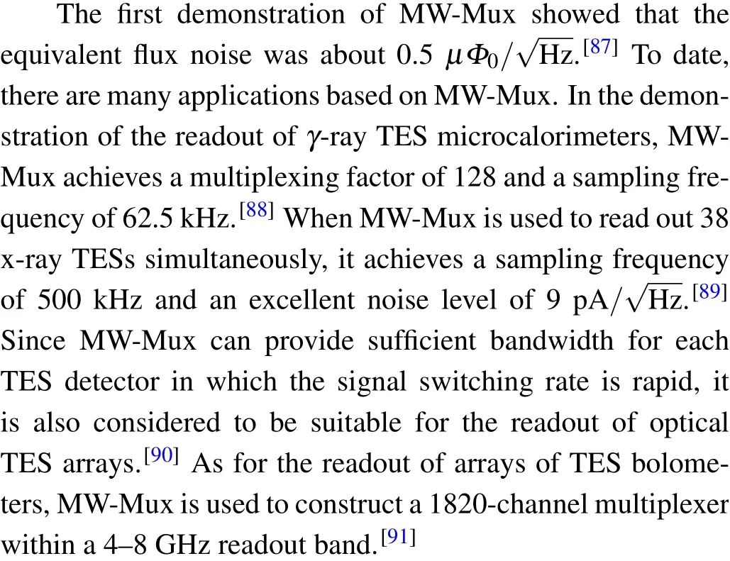
SQUID-based multiplexing technologies make the readout of large-scale TES arrays feasible. In order to advance SQUID-based multiplexing technologies over a wide frequency range, optimization and improvement for the entire readout system are required. Since each technology has its own advantages and disadvantages, finding a balance among its characteristics to realize a high-performance readout system is an important topic. Table 1 compares characteristics of different multiplexing technologies. When one multiplexing technology is applied to TES microcalorimeters and TES bolometers separately,the multiplexing factors of the two devices are different. Since TES microcalorimeters are used to detect x rays and gamma rays, and TES bolometers are used to detect sub-mm and microwave signals, they have different requirements for the pixel bandwidth. In general, TES microcalorimeters require larger pixel bandwidth than TES bolometers, which imposes restrictions on the multiplexing factor of TES microcalorimeters in the case that the total bandwidth of the readout system is limited. In Table 1, the multiplexing factors of TES microcalorimeters and TES bolometers are separately stated and the readout noise corresponds to the noise level achieved at the same multiplexing factor. The development goals of multiplexing technologies are to achieve large multiplexing factor while ensuring low readout noise of the entire system. Besides the multiplexing factor and the readout noise,some other characteristics such as the crosstalk,the chip area occupied by the filter element and the complexity of room-temperature electronics,also need to be taken into account in practical applications.

Table 1. Characteristics of different multiplexing technologies.
8. Summary
SQUID-based multiplexing technologies are compatible with a variety of cryogenic applications. This paper focuses on the multiplexed readout of TES arrays and reviews different types of multiplexing technologies including TDM,CDM,FDM and MW-Mux. Overall, SQUID-based multiplexing technologies are necessary for the readout of TES arrays.New applications that require large-scale TES arrays emphasize the importance of developing multiplexing technologies with large multiplexing factors and low readout noise. As advances continue in circuit architectures, room-temperature control and readout systems,SQUID-based multiplexing technologies are expected to meet the demands of future arrays of TES detectors.
Acknowledgements
Project supported by the National Science Foundation of China (Grant Nos. 11653001 and 11653004). The authors thank Changhao Zhao,Rutian Huang,Kaiyong He,Xiao Geng, Genting Dai and Liangliang Yang for valuable discussions.
猜你喜欢
肝博士(2022年3期)2022-06-30
初中生世界·九年级(2022年8期)2022-06-01
医学食疗与健康(2021年27期)2021-05-13
幸福家庭(2020年8期)2020-07-27
科学导报·学术(2020年17期)2020-05-22
家庭科学·新健康(2018年7期)2018-09-17
Coco薇(2017年5期)2017-06-05
Coco薇(2015年11期)2015-11-09
母子健康(2015年1期)2015-02-28
中国民族民间医药·下半月(2011年4期)2011-09-27
- Chinese Physics B的其它文章
- Formation of high-density cold molecules via electromagnetic trap
- Dynamics of molecular alignment steered by a few-cycle terahertz laser pulse
- Terahertz spectroscopy and lattice vibrational analysis of pararealgar and orpiment
- Molecule opacity study on low-lying states of CS
- Finite-time Mittag–Leffler synchronization of fractional-order complex-valued memristive neural networks with time delay
- Ultrafast Coulomb explosion imaging of molecules and molecular clusters