
Fabrication of honeycomb AuTe monolayer with Dirac nodal line fermions
2023-02-20 13:15QinWang汪琴JieZhang张杰JieruiHuang黄杰瑞JinanShi时金安ShuaiZhang张帅HuiGuo郭辉LiHuang黄立HongDing丁洪WuZhou周武YanFangZhang张艳芳XiaoLin林晓ShixuanDu杜世萱andHongJunGao高鸿钧
Chinese Physics B 2023年1期
Qin Wang(汪琴), Jie Zhang(张杰),Jierui Huang(黄杰瑞),Jinan Shi(时金安), Shuai Zhang(张帅),Hui Guo(郭辉), Li Huang(黄立), Hong Ding(丁洪),3,4, Wu Zhou(周武),3, Yan-Fang Zhang(张艳芳),†,Xiao Lin(林晓),3,‡, Shixuan Du(杜世萱),,3,4,§, and Hong-Jun Gao(高鸿钧),,3,4,¶
1School of Physical Sciences,University of Chinese Academy of Sciences,Beijing 100049,China
2Beijing National Center for Condensed Matter Physics and Institute of Physics,Chinese Academy of Sciences,Beijing 100190,China
3CAS Center for Excellent in Topological Quantum Computation,University of Chinese Academy of Sciences,Beijing 100190,China
4Songshan Lake Materials Laboratory,Dongguan 523808,China
Keywords: honeycomb lattices,transition-metal monochalcogenides,AuTe monolayer,two-dimensional(2D)
1. Introduction
Two-dimensional (2D) transition-metal chalcogenides(TMCs) have received remarkable attention in fundamental research[1–4]and practical applications,[5–9]primarily because of their simple forms,open-air stability and exceptional physicochemical properties. Up to now,2D TMCs have been revealed with various stoichiometric ratios,i.e.MX2,MX,andM2X(M:transition metal atoms,X:S,Se,and Te).Transitionmetal dichalcogenides (TMDs,MX2) have been thoroughly explored due to their unique properties[10–14]and the first transistor based on a monolayer MoS2.[15,16]Representative monolayer transition-metal monochalcogenides(TMMs,MX)are topological materials.[17–21]For example, an FeSe monolayer is a high-Tcsuperconductor,which can be used as an intrinsic Majorana platform.[21]2D transition-metal-rich TMCs(M2X)are predicted to be promising photocatalysts[22,23]and topological insulators.[24,25]Among the above TMCs, 2D TMDs can be easily derived from their parent layer-stacked bulk phases with weak van der Waal interaction, while 2D TMMs(MXandM2X)are difficult to exfoliate from 3D closepacked structures. As topological materials, 2D TMMs hold potential applications in high-speed low-dissipation nanodevices since monolayer CuSe[17]and its derivatives host topological nodal line fermions, thus attracting broad scientific interest despite the difficult synthesis.
Inspired by the fundamental research interest,[26–28]successful preliminary attempts for potential applications,[29,30]and limited experiment-realized Dirac nodal line fermion(DNLF)systems,[31–34]people show increasing enthusiasm at search and design of DNLF systems. To date, only a few 2D cases have been reported, such as 2D covalent organic frameworks (COFs),[35]Lieb lattices[36,37]and 2D pentagonal group-IVA chalcogenide materials.[38]In addition, theoretical calculation results suggest that monolayer CuSe,[17]AgTe[19]and AgSe[20]with honeycomb lattices show DNLF features which are protected by mirror reflection symmetry. These three candidates have been successfully fabricated with honeycomb structures on metal substrates,characterized by scanning tunneling microscopy (STM), low-energy electron diffraction (LEED), angle resolved photoemission spectroscopy(ARPES)techniques and first-principles calculations.However,ARPES results of monolayer CuSe,[17]AgTe[19]and AgSe[20]show that even the gapped nodal line feature induced by the symmetry broken is not observed due to the strong coupling between the monolayers and the substrates, which prevents their investigations in view of possible applications.Even in other 2D systems, experimental realizations of 2D DNLFs are limited to monolayer Cu2Si with a honeycomb Cu lattice and a triangular Si lattice[39]and tri-atomic layer Bi(110) in a brick phase.[40]Thus, it is desirable to search and fabricate new 2D Dirac nodal line materials which have a weaker interaction with substrates.
Here,we successfully fabricated monolayer gold telluride(AuTe) on Au(111) substrate by using molecular beam epitaxy (MBE) method. The monolayer AuTe was obtained by direct tellurization of an Au(111) substrate. The x-ray photoelectron spectroscopy(XPS)measurement displays that the Au–Te chemical bond forms in the top layer. The LEED characterization indicates that it is(2×2)AuTe on(3×3)Au(111)substrate. The atomic structure of the monolayer AuTe is determined by a combination of STM experiments, density functional theory (DFT) calculations and scanning tunneling electron microscopy (STEM) characterizations. DFT calculations suggest that a free-standing AuTe monolayer has two DNLFs protected by mirror reflection symmetry without spin–orbit coupling (SOC), different from the monolayer AuTe in the GaS crystal structure which is a topological insulator[41]and bulk AuTe2[42]in aPma2 space group which has been classified as a high symmetry line semi-metal. When considering SOC or buckling induced by the substrate, gaps are opened at the Dirac nodal lines due to the breaking of the mirror symmetry. It is noteworthy that the gapped nodal loops induced by the symmetry breaking have been observed by using ARPES.Compared with the reported gapped DNLFs realized in 2D metal monochalcogenides,AuTe monolayer makes it more promising for real applications in future nano-devices.
2. Results and discussion
The AuTe monolayer was fabricated by direct tellurizing an Au(111) substrate in an ultrahigh vacuum (UHV) roomtemperature(RT)STM–MBE equipment. Figure 1(a)demonstrates the schematic of the synthesis procedure of a monolayer AuTe on Au(111)surface. The Te atoms were firstly deposited on a clean Au(111)substrate at room temperature and then the sample was annealed to 530 K.When the growth process finished,the sample was transferred from the MBE chamber to the STM chamber for preliminary characterization.Figure 1(c) is a 100 nm×100 nm large-scale STM topographic image. The sample grows continuously across the two steps on the Au(111) surface, indicating a high quality. The possible Te adatoms on the sample make it form dense parallel strips. The two directions of the parallel strips are equivalent due to the symmetry of the sample and that of the Au(111)surface. Afterwards, the XPS measurements were performed to examine the formation of gold telluride. Figure 1(b)is the XPS spectrum of the Te 3d core level for the freshly deposited Te atoms on the Au(111) surface, which shows two peaks at 573.0 eV and 583.4 eV, corresponding to the two spin–orbit splitting components Te 3d5/2and Te 3d3/2,respectively. After annealing treatment,the two peaks of Te 3d5/2and Te 3d3/2shift to 572.7 eV and 583.1 eV,respectively. Compared to the elemental Te(before annealing),the negative 0.3 eV shift suggests that the Te atoms are in oxidation states,[43–46]indicating the formation of a gold telluride alloy.
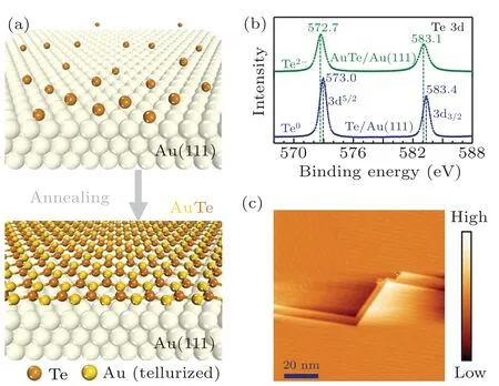
Fig.1. Growth process and XPS differences between AuTe and tellurium.(a)Schematic of the fabrication of AuTe thin films by direct tellurization of the Au(111)substrate. Au atoms in the Au(111)substrate and tellurized Au atoms are shown in light and golden yellow,respectively. (b)XPS measurements on binding energies of AuTe synthesized on the Au(111) substrate and Te deposited on Au(111) shown as normalized green and blue intensity curves,respectively. (c)Large-scale STM topography(U=-1.7 V and I=0.1 nA)at room temperature.
To further gain insight into the structure of the asfabricated material,we performed LEED and low temperature(4 K)STM characterization.The LEED pattern in Fig.2(a)reveals that the hexagonal diffraction spots of AuTe(red circles)have the same orientation as those of the Au(111) substrate(yellow circles), suggesting a rotational-domain-free growth.The(2×2)diffraction pattern of the monolayer AuTe,marked by white circles, corresponds to a well-defined Moir´e superstructure arising from the lattice mismatch between the AuTe monolayer and Au(111)substrate. Moreover, the same LEED patterns were observed on the entire sample surface(φ=10 mm in size),indicating a large-area and homogeneous monolayer AuTe.
Figure 2(b) displays an STM image representing the superstructure composed of the (2×2) AuTe monolayer on(3×3) Au(111) surface, with parallel strips formed which is possibly due to the lattice mismatch,the stress release process and adatoms. The zoomed-in STM image with atomic resolution in Fig.2(d)exhibits an obvious honeycomb lattice,and the average lattice constant isa1=4.3 ˚A(labelled by the red rhombus). Besides, a distinct (2×2) superstructure with respect to the AuTe lattice is also presented, with a periodicity of 8.6 ˚A, about twice ofa1(labelled by the white rhombus).Combined with the LEED pattern in Fig.2(a)and the inserted FFT image in Fig.2(d), the distinct(2×2)superstructure can be explained as the Moir´e pattern of (2×2) AuTe on (3×3)Au(111)surface. Besides,DFT calculations were also carried out to clarify the atomic structure of the sample.
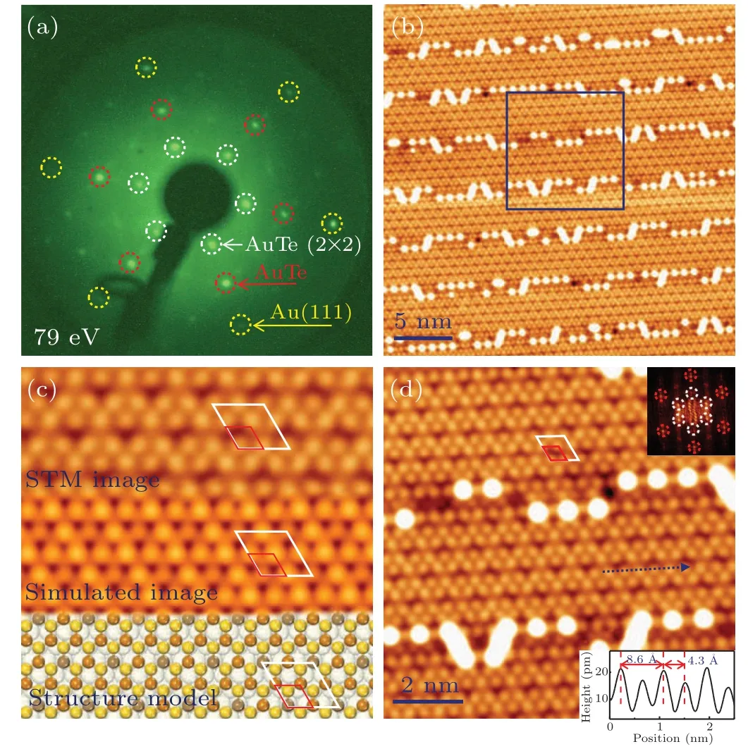
Fig.2. LEED patten and atomic configuration of AuTe monolayer on Au(111)substrate. (a)LEED patten. The yellow,red and white dashed circles indicate the diffraction spots from the Au(111)lattice,AuTe monolayer and(2×2)superstructure with respect to AuTe,respectively.(b)STM image(U =-1.5 V and I=0.15 nA)at 4 K shows the Moir´e pattern and domains of the AuTe monolayer on Au(111). The blue square marks the size of the close-up image in (d). (c) Atomic resolution STM image, simulated STM image, and the structure model of (2×2) superlattice (indicated by white rhombi) match each other. (d) High-resolution STM image (U = -1 V,I=0.1 nA)of AuTe monolayer, shows the honeycomb lattice of Te atoms in the topmost sublayer of the AuTe structure. The red and white rhombi denote the unit cell of the AuTe lattice and(2×2)superlattice,respectively.The inset displays the FFT pattern corresponding to AuTe and the superstructure in(a). The inset line profile along the blue dashed arrow shows a lattice periodicity of 4.3 ˚A.
Six possible atomic structures of AuxTeymonolayer have been considered,with their lattice information summarized in Fig.S1 and Table S1. Among all the possible structures,only AuTe structure is consistent with the STM results and the following STEM result. Since the simulated STM image corresponds to an ideal model(the bottom panel in Fig.2(c)),there is a tiny difference between the simulated STM image with the experimental ones. The well-reproduced Moir´e pattern,together with the lattice information in Fig.S1 and Table S1,demonstrate that the overlayer on the Au(111)surface is AuTe monolayer.
In order to further verify the structure of the monolayer AuTe on Au(111),cross-section high-angle-annular-dark-field(HAADF) STEM measurements were performed. The left panel of Fig. 3(a) is aZ-contrast atomically resolved STEM image of the AuTe/Au(111) interface, which manifests a monoatomic layer of the AuTe structure. The distances between neighboring atoms in the first layer and the second layer are 2.16 ˚A and 1.44 ˚A,respectively,in accordance with(2×2)monolayer AuTe on (3×3) Au(111) substrate. The relaxed model in the right panel of Fig.3(a)also matches well with the STEM image. The electron energy loss spectroscopy(EELS)mappings for the sample were also carried out(Figs.3(c)and 3(d)). It is obvious that Au and Te signals exist at the same layer, corresponding to the AuTe layer in the HAADF image in Fig. 3(b). By analyzing the EELS spectral intensity from Au element in Fig. S3, we exclude the delocalization effects of Au(111)substrates,which proves that monolayer AuTe has been fabricated on Au(111)surface.
Since monolayer CuSe, AgTe, and AgSe show DNLFs features, monolayer AuTe (Fig. S6a) is expected to also host mirror-symmetry-protected DNLFs(Fig.S6b). To further validate the mirror-symmetry-protected nodal loops, we investigate the AuTe monolayer with a buckled structure(Fig.4(a))which is relaxed on an Au(111)substrate.The side view shows that the substrate-induced buckling height is 0.39 ˚A.It should be noted that the Au(111)substrate is not taken into consideration for the band structure calculation. The green and red lines in Fig.4(b)describe the contribution from in-plane(Te px/pyand Au dxy/dx2-y2)and out-of-plane(Te pzand Au dxz/dyz)orbitals, respectively. These results clarify that the nodal loops are protected by mirror symmetry.

Fig.4. Calculated band structures and ARPES results. (a)Geometric structure of the(2×2)AuTe monolayer which is obtained after relaxation on an Au(111) surface. The side view shows the buckling height is 0.39 ˚A. (b) The calculated band structure of (a) with green and red curves illustrating contributions from in-plane and out-of-plane orbitals. (c) ARPES data obtained from the monolayer AuTe on Au(111) surface, superimposed with calculated band structure in(b). (d)The ARPES constant-energy contour at E=EF of a selected BZ(red hexagon). (e)and(f)ARPES intensity plots of cut 4(along K–Γ–K)and cut 7,which are indicated in(d)as dashed lines,respectively. For comparison,we overlay the calculated bands along K–Γ–K as blue lines on top of (e). The GDP indicates a gapped Dirac cone. (g) Energy distribution curves (EDCs) corresponding to the region indicated by black dashed rectangle in(e),with triangle marks highlighting the lower half of the Dirac cone.
ARPES is used to directly investigate the electronic properties of monolayer AuTe. The samples were transferred from the MBE chamber to the ARPES facility by a highvacuum suitcase. Figure 4(c) expresses the ARPES data of AuTe/Au(111) measured along the high symmetry directionM–K–Γ–Min the hexagonal Brillouin zone(BZ)with a photon energy of 40.8 eV. The ARPES spectrum is a mixture of monolayer AuTe and substrate-related signals resulting from the large penetration depth. The calculated band structure(shaded area in Fig. 4(b)) is embedded in Fig. 4(c) after an upward-shift by 1.46 eV. The upward-shift of 1.46 eV originates from the hole-doping effect of the AuTe monolayer(Fig.S4). The main features show good consistence with the ARPES experiment results.
The ARPES constant-energy contour atE=EFin Fig. 4(d) exhibits a ring-like feature with sixfold symmetry.However, the spectral intensity in the horizontal direction is suppressed due to the matrix element effect.[47,48]We selected two representative band cuts (black dash lines in Fig. 4(d))to demonstrate the distribution of Dirac nodal loop in the BZ (Figs. 4(e) and 4(f)). It shows clearly that the band dispersion is consistent with the calculated electronic structure(Fig.4(e)).Especially,the lower half of the gapped Dirac cone can be clearly seen from both the raw ARPES spectrum and energy distribution curves series plot in Fig. 4(g). The missing spectrum intensity of the upper half of Dirac cone may be due to the matrix element effect in ARPES experiment.[47,48]One can expect getting access to this part of band structure when a light source with different polarization or photon energy is used. In addition, the gapped Dirac point (GDP) is visible in all the ARPES intensity spectrums near the center of BZ(Fig.S5). The systematic ARPES results provide substantial evidence for the existence of the Dirac nodal loop in monolayer AuTe/Au(111). The gapped DNLF locates around 0.32 eV below the Fermi level,which is the first one observed by using ARPES technique in 2D metal monochalcogenides(CuSe,[17]AgTe[19]and AgSe[20]). Our realization of AuTe makes a step forward for real applications of 2D DNLFs.
3. Conclusions
By combining XPS, LEED, STM, STEM, ARPES techniques and DFT calculations, we confirm that AuTe monolayer with a honeycomb lattice has been successfully synthesized by directly tellurizing an Au(111) substrate. The nodal line character of monolayer AuTe has been revealed both experimentally and theoretically. Interestingly, the symmetrybroken-induced gapped nodal loops are experimentally observed which is absent for other reported 2D transition-metal monochalcogenides with DNL characters. Thus, we propose that monolayer AuTe exhibits appealing interest for future transport measurement and nano device applications.
4. Methods
Sample preparation and characterizations Monolayer AuTe films were grown in an ultrahigh vacuum(UHV)chamber, with a base pressure of 1×10⁻⁹mbar, equipped with standard MBE capabilities. First, the Au(111) substrate was cleaned by several cycles of Ar+ions sputtering followed by annealing until sharp diffraction spots in the LEED pattern and clean surface terraces with a herringbone reconstruction in the STM images were obtained. Then, tellurium atoms (Sigma 99.999%)were evaporated from a Knudsen cell and deposited onto the substrate at room temperature. Subsequently, the sample was annealed up to 530 K to achieved tellurization and crystallization. The growth process was monitored by LEED.After growth,the sample was transferred to an STM chamber(2×10⁻¹⁰mbar) for imaging and to an ARPES chamber for characterizing the electronic properties.
ARPES measurement The ARPES measurements were performed at the Institute of Physics,Chinese Academy of Sciences, using a R4000 analyzer and a helium discharge lamp,under ultrahigh vacuum better than 3×10-11Torr. The data were recorded with He IIαphotons at 15 K. The energy and angular resolutions were set to 10 meV and 0.1°,respectively.The Fermi level of the samples was determined from a polycrystalline gold reference in electronical contact with the sample.
STEM characterization The sample was transferred from the UHV chamber to the atmosphere, and then covered with graphite.
Calculations In this work,all calculations are performed using the Viennaab initiosimulation package (VASP)[49,50]based on density functional theory (DFT) with the projector augmented-wave (PAW)[51]method and the local density approximation (LDA)[52,53]for the exchange–correlation functional. The energy cutoff of the plane wave basis set is 400 eV.The monolayer AuTe is fully relaxed until the forces on the ions are less than 0.001 eV/˚A and the energy difference is less than 10-6eV. For the AuTe/Au(111) system, the criteria for force and energy convergence are 0.05 eV/˚A and 10-4eV,respectively. The vacuum distance between two adjacent supercells inzdirection is larger than 15 ˚A.Thek-points samplings are (21×21×1) for the monolayer AuTe and (11×11×1) for that on Au(111) with the Gamma scheme, respectively. The van der Waals interaction is described by the optB86b-vdw functional[54–56]for the AuTe/Au(111) system. The simulated STM image is obtained based on the Tersoff-Hamann approximation.[56]
Acknowledgements
Project supported by the National Key R&D Program of China (Grant No. 2018YFA0305800), the National Natural Science Foundation of China (Grant Nos. 61925111,61888102, and 52102193), the Strategic Priority Research Program of Chinese Academy of Sciences (Grant Nos. XDB28000000 and XDB30000000), CAS Project for Young Scientists in Basic Research (Grant No. YSBR-003),and the Fundamental Research Funds for the Central Universities.
猜你喜欢
故事会(2022年7期)2022-04-03
中国核电(2021年3期)2021-08-13
创新作文(3-4年级)(2019年12期)2019-12-17
艺术大观(2019年11期)2019-11-12
艺术大观(2019年19期)2019-10-12
艺术大观(2019年16期)2019-10-09
数学大王·趣味逻辑(2019年9期)2019-10-09
艺术大观(2019年14期)2019-09-28
创新作文(小学版)(2019年35期)2019-01-11
文理导航·趣味课堂(2017年5期)2018-02-12

- Chinese Physics B的其它文章
- The coupled deep neural networks for coupling of the Stokes and Darcy–Forchheimer problems
- Anomalous diffusion in branched elliptical structure
- Inhibitory effect induced by fractional Gaussian noise in neuronal system
- Enhancement of electron–positron pairs in combined potential wells with linear chirp frequency
- Enhancement of charging performance of quantum battery via quantum coherence of bath
- Improving the teleportation of quantum Fisher information under non-Markovian environment