
Effects of preparation parameters on growth and properties of β-Ga2O3 film
2023-02-20 13:15ZiHaoChen陈子豪YongShengWang王永胜NingZhang张宁BinZhou周兵JieGao高洁YanXiaWu吴艳霞YongMa马永HongJunHei黑鸿君YanYanShen申艳艳ZhiYongHe贺志勇andShengWangYu于盛旺
Chinese Physics B 2023年1期
Zi-Hao Chen(陈子豪), Yong-Sheng Wang(王永胜), Ning Zhang(张宁), Bin Zhou(周兵),Jie Gao(高洁), Yan-Xia Wu(吴艳霞), Yong Ma(马永), Hong-Jun Hei(黑鸿君),Yan-Yan Shen(申艳艳), Zhi-Yong He(贺志勇), and Sheng-Wang Yu(于盛旺)
College of Materials Science and Engineering,Taiyuan University of Technology,Taiyuan 030024,China
Keywords: β-Ga2O3,magnetron sputtering,growth parameters,optical and electrical properties
1. Introduction
With the excellent physicochemical properties, the wide bandgap semiconductor materials(such as SiC,GaN,AlGaN)are very suitable for high-temperature, high-frequency, and high-power semiconductor devices including diodes, detectors, and high-power electronic devices.[1–3]However, these devices are rarely able to go out of the laboratory and enter into industrialization because of the high cost of fabrication. Therefore, to reduce the cost of wide bandgap semiconductor devices is necessary for their practical application.As a wide bandgap semiconductor, Ga2O3has a band gap of~4.9 eV, a Baliga’s figure of merit (BFOM) of 3400, and a breakdown field strength of 8 MV/cm.[4]Compared with SiC or GaN, the single-crystal Ga2O3wafer with a size of 4 inch(1 inch=2.54 cm)has been synthesized by using several standard melt growth methods.[5]The polycrystalline Ga2O3film has similar semiconductor characteristics to and lower fabrication cost than single crystal,these advantages make Ga2O3receive increasing attention in the field of electroluminescent devices,[6,7]gas sensitive sensors,[8–10]photodetectors,[11–13]field-effect transistor,[14–16]etc.
The crystal structures of Ga2O3, includingα,β,γ,δ,andε, could transform into each other under given conditions.[17]Among them,defects in the growth ofβ-Ga2O3thin film include VO(oxygen vacancy), Oi(oxygen interstitial),VGa(gallium vacancy), and Gai(gallium interstitial) due to a monoclinic crystal with theC2/mspace group. Owing to the VOand Gaiwith the lower formation energy,[18]β-Ga2O3is prone to forming oxygen vacancies and gallium interstitial during growth. Therefore, theβ-Ga2O3, as a most stable phase,has aroused extensive interest in the semiconductor devices due to its promising future in the industrial application. Sasakiet al. found that the Pt/β-Ga2O3Schottky diode fabricated by the floating-zone has a Schottky barrier height in a range of 1.3 eV–1.5 eV.[19]Shimboriet al. reported that NiO/β-Ga2O3heterojunction diode has a higher breakdown voltage and lower leakage current than Ni/β-Ga2O3Schottky diodes.[20]Ohet al.reported that aβ-Ga2O3MSM photodetector with the transparent graphene electrode increases the photosensitive area and rejection ratio of the photodetector.[21]Zhanget al.reported that single-crystalline sphericalβ-Ga2O3particles with an average diameter of~200 nm are expected to be used in white-LED phosphors due to the blue–green and red–light emission.[22]Many methods have been used to prepare theβ-Ga2O3film and adjust defects. Greenet al.found that theβ-Ga2O3field-effect transistor fabricated by metal–organic vapor phase epitaxy has a gate-to-drain electric field of~3.8 MV/cm.[23]Moreover, Chenet al. found that the growth ofβ-Ga2O3film is dependent on the oxygen pressure of pulsed laser deposition,such as mainly along(201)plane at an oxygen pressure of 0.5 Pa, but along (400) plane for oxygen pressure in a range from 0.5 Pa to 2 Pa.[24]Chenet al.reported that the pressure ofβ-Ga2O3film can affect the preferred orientation and growth rate by metal–organic chemical vapor deposition on GaAs substrate.[25]Shihet al.found that theβ-Ga2O3MOS-HEMT has excellent performance caused byβ-Ga2O3gate dielectric and surface passivation layer.[26]Liaoet al.found that the crystal quality ofβ-Ga2O3film can be adjusted by RF magnetron sputtering under growth pressure in a range of 0.5 Pa–3 Pa,resulting in a similar variation trend to that of the optical bandgap ofβ-Ga2O3film.[27]Ma and Fan preparedβ-Ga2O3nanomaterials by the thermal evaporation method,and found that the photoelectric properties of the nanomaterials change due to the oxygen existing.[28]Based on these results, the preparation method and parameter have important effects on the growth and properties of theβ-Ga2O3film.
In this work,the Ga2O3films are prepared on the silicon and quartz substrates by radio frequency(RF)magnetron sputtering, then transformed intoβ-Ga2O3by annealing. The effects of preparation parameters on the structure and properties ofβ-Ga2O3film are studied by tailoring argon–oxygen flow ratio,sputtering power,sputtering time and annealing temperature.
2. Experimental details
The Ga2O3films were fabricated on the surface of(100) silicon substrates by the RF magnetron sputtering method. The monocrystalline silicon wafers were ultrasonically cleaned in ethanol solution for 10 min and washed with deionized water and dried, then placed into the deposition chamber of magnetron sputtering apparatus. In order to remove impurities from the surface of gallium oxide target as much as possible, the pre-sputtering was carried out in argon atmosphere for 5 min, then the presetting sputtering power and gas flow were adjusted. The atmospheric pressure of the chamber was adjusted to 0.8 Pa by controlling the outlet valve.A small amount of O2is added in addition to argon to improve crystallinity of the film and reduce internal defects.[29]Under the combined action of electric field, magnetic field and argon particles, gallium particles in the target were bombarded and reacted with oxygen to form amorphous Ga2O3film on the substrate. Theβ-Ga2O3film was obtained after being annealed.[30]The effects of preparation parameters including argon–oxygen flow ratio,sputtering power,sputtering time and annealing temperature on the growth and properties ofβ-Ga2O3thin films were studied as shown in Table 1. All samples were annealed in air for 120 min. In each experiment,a quartz substrate (optical transmittance>90%) was placed in the sputtering system so as to be used for characterizing the optical properties of the films.

Table 1. Detailed growth parameters of β-Ga2O3 thin films. AO:argon–oxygen flow ratio,SP:sputtering power,Pre:sputtering pressure,ST:sputtering time,AT:annealing temperature.

Fig.1. Schematic diagram of preparation process of β-Ga2O3 thin films.
The metal electrodes were prepared on the film to study the electrical property. Theβ-Ga2O3film samples were ultrasonically cleaned in ethanol solution for 5 min,then rinsed with deionized water and dried. The Ti could form Ohmic contact withβ-Ga2O3under a certain condition.[31]The metal electrodes were obtained by depositing Ti(40 nm)/Ag(80 nm)on the surface of sample by vacuum evaporation via a special mask. Each electrode has a size of 1 mm×1 mm and the spacing between adjacent electrodes is 2 mm. The samples with metal electrodes were annealed in air for 30 s at 400°C.Figure 1 shows a schematic diagram of the preparation process and the final product.
The crystal structure ofβ-Ga2O3were characterized by x-ray diffraction (XRD, Smartlab X, Rigaku). The morphology ofβ-Ga2O3and Ti/Ag electrodes were characterized by scanning electron microscope (SEM, ZEISS GeminiSEM 300). The optical properties were obtained by UV-vis spectrophotometer(Agilent cary 100). TheI–Vcurve of the films were measured by Hall effect measurement(Lake shore 8400 Series).
3. Results and discussion
Figure 2 shows the XRD patterns of Ga2O3films deposited under different conditions. The broad diffraction patterns of Ga2O3samples indicate the amorphous structures under different argon–oxygen flow ratios (Fig. 2(a)). The obvious diffraction peaks at 30.5°, 35.2°, and 64.7°correspond to (¯401), (111), and (403) planes ofβ-Ga2O3by examining the standard card of JCPDS43-1012, and superimpose on the broad diffraction pattern of the amorphous Ga2O3, suggesting that the amorphous Ga2O3films have transformed intoβphase after being annealed.The oxygen content increases with the argon–oxygen flow ratio dropping, leading to the shift of diffraction peak in the crystal plane of(403). The crystal lattice contains the increased amount of VOunder the hypoxia environment,and in an oxygen-rich environment,enough oxygen atoms exist as Oi, leading to the lattice distortion. When the sputtering power is 140 W (Fig. 2(b)), the crystal plane of (¯401) dominates the process of crystallization. With the increase of sputtering power, the diffraction peak in the crystal plane of (111) instead of in the crystal plane of (¯401) is enhanced, indicating the preferential growth of the film. According to the Scherrer formula[32]
whereDis the grain size perpendicular to the lattice plane,kis the Scherrer constant with a value of 0.9,λis the wavelength of x-ray radiation,Bis the full width at half maximum(FWHM)of diffraction peaks,andθis the corresponding Bragg angle. Here, the FWHM of the diffraction peak at crystal plane of(¯401)increases with the augment of sputtering power(Fig.2(b)),indicating that the grain size decreases. The increase of sputtering power leads to a strong bombardment effect. So,more atoms bombarded out of Ga2O3target result in more deposited-nanocrystals.

Fig.2. XRD patterns of β-Ga2O3 films deposited under different parameters: (a)argon–oxygen flow ratio;(b)sputtering power;(c)sputtering time;(d)annealing temperature.
Moreover,as the sputtering time increases(Fig.2(c)),the intensities of diffraction peaks increase. Specially,the diffraction peaks appear at 19.0°and 59.2°corresponding to the crystal planes of (¯201) and (¯603) for 150 min. As for samples of the different annealing temperatures(Fig.2(d)),the diffraction peaks at 30.5°and 64.7°superimpose on the broad diffraction pattern of the amorphous Ga2O3for sample annealed at 600°C.With the temperature increasing to 900°C,the diffraction peaks are enhanced in(111),(¯201),(002),and(401)crystal planes. We find that each crystal plane of all samples annealed at 600°C shows the low diffraction peak intensity and the large FWHM,but the diffraction peak intensity of samples annealed at 900°C all increase(Figs.2(a)–2(d)). It means that the crystallinity ofβ-Ga2O3films increases with the annealed temperature rising.

Fig.3. (a)Cross-sectional SEM image of β-Ga2O3 film and(b)plot of thickness versus sputtering time, sputtering power, and argon–oxygen flow rate of β-Ga2O3 film.
Figure 3(a) shows the cross-sectional morphology ofβ-Ga2O3film. Theβ-Ga2O3film has the uniform and dense cross-sectional morphology without internal holes. Under this preparation condition, the thickness of theβ-Ga2O3film is 197.2 nm. Moreover, the thickness values of theβ-Ga2O3films at various preparation parameters are summarized via the cross-sectional image(Fig.3(b)). Obviously,the thickness of theβ-Ga2O3film increases with the increase of the argon–oxygen flow ratio, sputtering power and time. The annealing temperature has almost no influence on the thickness of the film(not shown). With the enlargement of argon–oxygen flow ratio,more argon particles bombard Ga2O3target,resulting in the increase of growth rate. Moreover, with the increase of sputtering power,more Ga2O3particles are generated and react with the oxygen due to the enhanced bombardment effect on the Ga2O3target,resulting in the increased thickness of the film.
Figure 4(a)shows the surface morphologies ofβ-Ga2O3films annealed at different temperatures. The flat surface morphologies of films annealed at 600°C shows small grains of Ga2O3, which are due to the incomplete crystallization. The formation of small nanocrystalline grains forβ-Ga2O3can be confirmed by the weaker diffraction peak intensity and larger FWHM (Fig. 2(d)). With the increase of annealing temperature,the crystallinity of the film can be greatly improved,and the obvious spherical protrusions can be observed on the surface of sample annealed at 800°C.When the annealing temperature is further increased to 900°C, the spherical grains on the surface become dense, and more spherical grains with diameters ranging from 20 nm to 30 nm form.
The 3D contour image of the sample surface is characterized, and the roughness-related parameters are obtained as follows: average roughness (Ra), maximum peak of contour(Rp)and minimum valley of contour(Rv). Figure 4(b)shows the 3D contour image of the sample annealed at 600°C, the overall surface of the film is smooth and flat without obvious pits and spikes, which is consistent with the scenario of SEM image in Fig. 4(a). With the enlargement of argon–oxygen flow ratio(Fig.4(c)),theRaof the film first decreases,then increases. A minimumRa-value can be obtained at an argon–oxygen flow ratio of 8:1. The higherRa-value means the oxygen-deficient situation, which is caused by stronger bombardment of the film surface at low oxygen content. The growth rate ofβ-Ga2O3thin film slows down with the increase of oxygen content. Moreover, the oxygen-rich environment reduces surface defects of the films. However, with the increase of sputtering power, theRa-value decreases by nearly half, thus improving the surface quality. The increased sputtering power means the strengthening of bombardment effect,which improves the adatom mobility and contributes to the surface quality of film. There has little effect on theRa-values of samples annealed at different temperature,but the values ofRpandRvincrease with the annealing temperature increasing(Rp:7.8 nm→145.9 nm;Rv: 43.5 nm→-245.2 nm). With the increase of sputtering time, theRaofβ-Ga2O3thin film increases gradually to 2.8 nm at 150 min. The increase of time can lead to the accumulation of defects to accumulate,resulting in uneven distribution of grains on the surface.

Fig.4. (a) Top-view SEM images of β-Ga2O3 thin films annealed at different temperatures, (b) three-dimensional (3D) contour image of β-Ga2O3 thin film annealed at 600 °C for 120 min,(c)plot of average roughness(Ra)versus argon–oxygen flow ratio and sputtering power,and(d)plot of average roughness versus annealing temperature and sputtering time of β-Ga2O3 thin films.
Figure 5(a) shows the SEM cross-section image of the prepared electrode structure.By combining the EDS results of the cross-section (Fig. 5(b)), the obvious layered structure of Ag/Ti/Ga2O3/Si-substrate can be confirmed. The O element not only exists in the gallium layer, but also penetrates into the Si layer and diffuses into the Ti/Ag electrode after being annealed (EDS result). In addition, Si also diffuses toward the Ga2O3layer,which has a similar mechanism to that of Si dopedβ-Ga2O3affecting the bandgap ofβ-Ga2O3thin films.
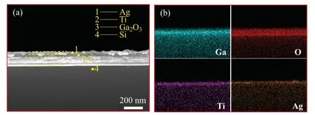
Fig.5. (a) Cross-section SEM image of prepared electrode structure, and(b)corresponding EDS mapping element distributions.
Figure 6 shows the optical transmittance spectra of currentβ-Ga2O3films at different preparation parameters. Allβ-Ga2O3films display the good optical transmittances in the visible range of 380 nm–780 nm. An obvious absorption edge appears near to 250 nm, which indicates thatβ-Ga2O3films are suitable for the detection of UVC.Fabry–Perot oscillation of the transmission curve implies good interface quality betweenβ-Ga2O3films and substrates.[33]The optical transmittance of the film is enhanced with the increase of sputtering power and annealing temperature, which is related to the improvement of film quality. Moreover,it is notable that the absorption edge has a red shift with the increase of sputtering time and power. Since main defects of VOaccumulate in the process of deposition and growth of film, these VOexist in the energy band as the donor energy, leading to the shifting of band structure. As Liet al.[34]believed, that was a degradation of quantum size effect. Becauseβ-Ga2O3is a direct bandgap semiconductor,[35]the bandgap ofβ-Ga2O3thin film can be calculated from Tauc formula[36]

whereαis the absorption coefficient,hνis the incident photon energy,Ais the constant,andEgis the bandgap,the value ofEgcan be derived by fitting the linear region of the(αhν)2versus hνplot and taking the intercept on thehν-axis(Fig.6). Here,the bandgap of theβ-Ga2O3decreases with the decrease of oxygen,which can be attributed to the increase of point defects dominated by oxygen vacancies. In addition,the bandgap also gradually decreases with the increase of sputtering power and annealing temperature. In short,the surface quality can be improved by increasing the sputtering power,resulting in the reducing bandgap;the crystal quality increases with the increase of temperature,leading to the decrease of bandgap. All these results indicate that the bandgap ofβ-Ga2O3films is affected by the film quality.
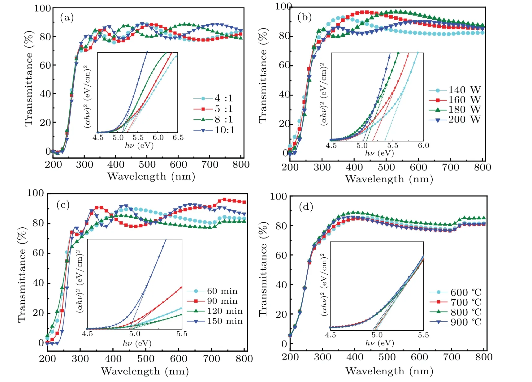
Fig.6. Variations of optical transmittance spectra of β-Ga2O3thin films: with(a)argon–oxygen flow ratio,(b)sputtering power,(c)sputtering time,and(d)annealing temperature,with inset showing variations of(αhν)2 with photon energy(hν).

Fig.7. (a) The I–V curves of β-Ga2O3 thin films annealed at different temperatures and (b) current flowing through the thin film versus annealing temperature at a bias voltage of 1 V.
TheI–Vcurves ofβ-Ga2O3thin films at different growth parameters are tested. The sample annealed at 900°C shows the Ohmic behavior between Ti andβ-Ga2O3,and the remaining samples exhibit the Schottky contact behavior(Fig.7(a)).Moreover,the forward/reverse current at 1-V bias voltage are calculated (Fig. 7(b)). The current flowing through theβ-Ga2O3film increases almost with the increase of annealing temperature,indicating that the resistance of the film gradually decreases. It is closely related to the crystallization quality of the film (Fig. 2(d)). There is a higher intensity of diffraction peak and a smaller FWHM at 900°C, thus the currents can flow across the grain boundaries.[37]
TheEg-values obtained at different preparation parameters are calculated in Fig. 8(a). TheEg-value represents the distance from the top of valence band to the bottom of conduction band in the band structure,which varies from 4.94 eV to 5.34 eV depending on the preparation process. However,almost all samples(except for the sample annealed at 900°C)are of Schottky contact,indicating that the formation of Ohmic contact is not just related to the band gap of the film. In fact,for n-type intrinsic semiconductor such asβ-Ga2O3,the formation of Ohmic contact depends on the Schottky barrier heightφB:

whereφMis the metal work function, andχsis the electron affinity of the semiconductor. Usually, theφBwith a negative value is achieved by choosing a metal of lowφMat the constantχs(4.00±0.05 eV),named Ohmic contact.[38]However,theφBofβ-Ga2O3does not rely onφMdirectly because of the surface states, metal-induced gap-states and near surface defects.[39]Previous report found that there can be the upward bending of the band onβ-Ga2O3surface,[40]causing the contacts formed betweenβ-Ga2O3and metals to be always Schottky contacts(Fig.8(b)). The Ohmic contact between the metal andβ-Ga2O3forms at 900°C temperature. As mentioned above,the point defects inβ-Ga2O3film are dominated by oxygen vacancies,thus introducing additional defect levels into the band structure. However, it is too deep to be excited according to previous report,so it is not generally considered to be the source of charge carriers. When the annealing temperature reaches 900°C,the high temperature provides a large amount of energy for the thermal motion of the electrons,thus leading a large number of electrons to be excited and transit to the conduction band. So, the Ohmic contact is achieved through the tunneling effect.

Fig.8. (a)The Eg values of β-Ga2O3 thin films at different growth parameters,(b)energy band of Schottky contact between Ti and β-Ga2O3,and(c)mechanism for Ohmic contact formation annealed at 900 °C.
4. Conclusions
Theβ-Ga2O3thin films are prepared on the silicon substrates by RF magnetron sputtering method. The effects of preparation parameters are studied including argon–oxygen flow ratio, sputtering power, sputtering time and annealing temperature. The annealing temperature plays a vital role in the crystallinity of theβ-Ga2O3film. The thickness ofβ-Ga2O3films depend on argon–oxygen flow ratio, sputtering power and sputtering time. The surface roughness of Ga2O3film increases with the augment of argon–oxygen flow ratio and sputtering time,while decreases with the sputtering power increasing. The transmission spectra of the films are tested by UV-vis, and the bandgap are calculated according to the Tauc formula. The bandgap is closely related to the quality of the film and affected by the number of oxygen vacancy defects. The Ti/Ag electrode is deposited on the surface of the films for testing theI–Vcurve. Ohmic contact is obtained at 900°C, which is probably related to the transition behavior of electrons at the defect level when gain enough energy. The resistance of the film is reduced by increasing the annealing temperature because of the improved crystallinity.
Acknowledgements
Project supported by the Science and Technology Major Project of Shanxi Province,China(Grant No.20181102013),the “1331 Project” Engineering Research Center of Shanxi Province, China (Grant No. PT201801), and the Natural Science Foundation of Shanxi Province, China (Grant No.201801D221131).
猜你喜欢
大江南北(2022年11期)2022-11-08
民族文汇(2022年20期)2022-05-29
共产党员·下(2022年4期)2022-05-17
阅读(快乐英语中年级)(2022年3期)2022-03-30
颂雅风·艺术月刊(2021年4期)2021-12-24
小学生学习指导(高年级)(2021年10期)2021-11-02
中学生英语·中考指导版(2021年2期)2021-05-24
中学生英语·中考指导版(2021年3期)2021-05-24
科学与财富(2021年34期)2021-05-10
疯狂英语·读写版(2019年5期)2019-09-10
- Chinese Physics B的其它文章
- The coupled deep neural networks for coupling of the Stokes and Darcy–Forchheimer problems
- Anomalous diffusion in branched elliptical structure
- Inhibitory effect induced by fractional Gaussian noise in neuronal system
- Enhancement of electron–positron pairs in combined potential wells with linear chirp frequency
- Enhancement of charging performance of quantum battery via quantum coherence of bath
- Improving the teleportation of quantum Fisher information under non-Markovian environment