
Skyrmion-based logic gates controlled by electric currents in synthetic antiferromagnet
2023-02-20 13:16LinlinLi李林霖JiaLuo罗佳JingXia夏静YanZhou周艳XiaoxiLiu刘小晰andGuopingZhao赵国平
Chinese Physics B 2023年1期
Linlin Li(李林霖), Jia Luo(罗佳), Jing Xia(夏静), Yan Zhou(周艳),Xiaoxi Liu(刘小晰), and Guoping Zhao(赵国平),4,†
1College of Physics and Electronic Engineering,Sichuan Normal University,Chengdu 610068,China
2Department of Electrical and Computer Engineering,Shinshu University,Wakasato 4-17-1,Nagano 380-8553,Japan
3School of Science and Engineering,The Chinese University of Hong Kong,Shenzhen 518172,China
4Center for Magnetism and Spintronics,Sichuan Normal University,Chengdu 610068,China
Keywords: skyrmions,logic gates,synthetic antiferromagnets,micromagnetic simulation
1. Introduction
Various ways have been proposed to realize the motion of skyrmions in a racetrack,[33–36]including the spinpolarized current, the temperature gradient, the magnetic anisotropy gradient,etc.[29,37,38]However, the ferromagnetic(FM) skyrmion will exhibit a lateral drift during the motion (i.e., the skyrmion Hall effect) due to the presence of Magnus force,[39–41]which may cause the annihilation of skyrmions at the racetrack edge and thus destroy the information.[29]Therefore, interest has been devoted to SAF skyrmions that can effectively suppress the skyrmion Hall effect without affecting the topological protection.[31,42–45]Up to now, there are many logic devices that have been designed based on skyrmions and domain wall (DW) dynamics in nanotrack, such as the reversible conversion and the collision between the skyrmion and the domain wall,[23,24,26,46,47]skyrmion–skyrmion collision,[27,40,48–50]skyrmion Hall effect and skyrmion–edge repulsion.[40]Compared with the most investigated FM skyrmions and domain wall, the racetrack memory and logic devices based on SAF skyrmions exhibit five distinctive characteristics. Firstly, SAF skyrmions can move straight along the spin-polarized current without the skyrmion Hall effect.[42]Secondly,it can robustly protect the magnetic perturbation as the net magnetization of skyrmion is zero.[42]Thirdly, SAF skyrmion can move at higher velocity driven by spin currents than FM skyrmion and domain wall.[31]Fourthly, logic devices only use skyrmion’s motion and interaction without the reversible conversion between skyrmions and DW,which can effectively decrease the complexity of logic implementation.[27,28]Fifthly, the SAFskyrmion-based logic gates can simplify the driving mode of devices, reducing energy consumption, enhancing the motion speed of skyrmion and increasing the types of logic functions.[30]
In this work,we have analyzed the skyrmion motion velocity of SAF skyrmion in SAF racetracks and found the velocity can be influenced by the edge and driving force,[46,51]which agrees very well with the simulation results. Further,we computationally propose a complete logic gate on SAF skyrmions including AND,OR,NOT,NOR,XOR,and NAND gates by utilizing the spin–orbit torque,[52–54]skyrmion Hall effect,[42,55,56]skyrmion–skyrmion repulsion, and skyrmion–edge interaction.[40,57]In the SAF bilayer, we show that bilayer-skyrmion can travel along the racetrack at a high speed driven by spin current,which is beneficial to simplify the operation of skyrmion-based devices.
2. Model and methods
Figure 1(a) illustrates the proposed structure, which is composed of two perpendicularly magnetized FM layers strongly coupled via the antiferromagnetic (AFM) interface interaction with a heavy metal layer beneath the bottom FM layer.[42]For the current-induced SAF skyrmion dynamics,we apply electric current in the +xdirection in the heavy metal(HM)layer to produce a vertical spin current to the magnetic layer and numerically solve the modified Landau–Lifshitz–Gilbert(LLG)equation including the damping-like spin–orbittorque in the simulation. Here,the time-dependent magnetization dynamics is thus governed by[29,58]
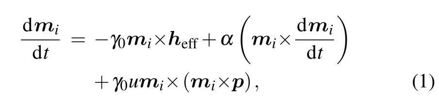
whereℎeff=-∂Htotal/μ0Ms∂miis the effective magnetic field induced by the free energy density of the system,μ0is the vacuum magnetic permittivity andMsis the saturation magnetization.mirepresents the local magnetic moment orientation,γ0is the gyromagnetic ratio andαis the Gilbert damping coefficient,andp=-represents a spin polarization vector.

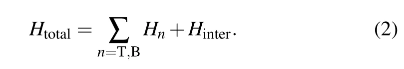
is the damping-like spin–orbit-torque coefficient with ¯has the reduced Planck constant,eis the electron charge,jis the applied driving current density,θSH=0.1 is the spin Hall angle,ais the film thickness of FM layer. For the total HamiltonianHtotal, we consider the Hamiltonian of each FM layerHnand the interlayer AFM exchange couplingHinterbetween the top and bottom FM layers,[42,59]which can be written as
The Hamiltonian for each FM layer can be written as follows:

wherenis the FM layer index (n=T, B represents the top layer and bottom layer, respectively),denotes the local magnetic moment orientation normalized as=1 at the sitei, and the〈i,j〉runs over all the nearest-neighbor sites in each FM layer. The first term represents the intralayer FM exchange interaction with FM exchange stiffnessAintra. The second and third terms represent the perpendicular magnetic anisotropy with the anisotropy constantKand the DMI with the DMI vectorD, respectively, whileHDDIrepresents the dipole–dipole interaction. The Hamiltonian for the interlayer AFM exchange interactions can be written as follows:
什寒村是海南岛上海拔最高的村庄之一。什寒村之所以拥有天然氧吧的称号,而且适宜居住、养生、旅游等,是因为这里优质的空气。什寒村处于海南三大河流之一的昌化江流域,拥有茂盛的森林、众多的溪流,每一立方米含30000个至40000个负氧离子。同时还拥有许多丰富的资源如生态旅游资源、健康养生资源等,被比喻为"天上什寒"、"天然氧吧"。
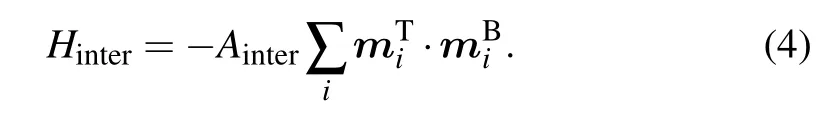
The symbol ofAinteris negative for the interlayer AFM interaction, where we assume that spins in the top FM layer are pointing upward and the spins in the bottom FM layer are pointing downward owing to the interlayer AFM exchange coupling. The strong antiferromagnetic coupling results in the two FM layers having opposite magnetization configurations,which plays a key role in eliminating the skyrmion Hall effect.[60]
Here, we simulate the SAF skyrmion logic functions using the Object Oriented Micromagnetic Framework(OOMMF) with an extended module of the Dzyaloshinskii–Moriya interaction.[61]For micromagnetic simulations, the standard magnetic material parameters of Co/Pt multilayers are used for the SAF structure:[27,29,42,45,59]MS=580 kA·m-1,K= 0.65 MJ·m-3–0.85 MJ·m-3with a default value ofK= 0.8 MJ·m-3,Aintra= 15 pJ·m-1,D=2.9 mJ·m-2–3.3 mJ·m-2with a default value ofD=3 mJ·m-2, antiferromagnetic coupling strengthAinter=4 mJ·m-2,γ0=2.211×10⁵m·(A·s)-1,α=0.3. Considering the balance between the numerical accuracy and computational efficiency, all the cell size used in this simulation is 2 nm×2 nm×1 nm.
For the steady motion of skyrmion in the proposed SAF logic gates, we use the Thiele equation to interpret the simulation results of isolated skyrmion.[46,51,62,63]The currentinduced skyrmion motion in a bilayer nanotrack can be written as
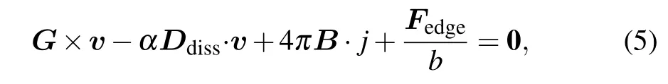
wherev,α,Ddiss,andBrepresent the skyrmion velocity,the damping constant,the dissipative tensor,and the tensor related to the driving current,respectively. In the fourth term,Fedgeis the external force that includes the joint repulsive force from the tilted edge and notches,where the constantb=μ0aMs/γ0.G=(0,0,-4πQ) is the gyromagnetic coupling vector, withQbeing the skyrmion topological number.[64]The skyrmion number in each FM layer can be defined as

The dissipative tensor can be written as
withFx-edgeandFy-edgerepresenting edge forces in thexandydirections,respectively. For the rigid magnetic skyrmion in this work,we always haveDxx=Dyy=Ddiss,Ixy=-Iyx=I,and the value ofIandDdissare positive. Namely, the motion equation of isolated SAF skyrmion can be rewritten into the following form

where the spin-polarized current flows along thexdirection(jy=0). Considering the steady motion of skyrmion along the nanotrack, boundary forces in thexandydirections can be ignored. Further,the topologic number of the SAF bilayer skyrmion is zero and the velocity could be simplified as

According to Refs. [51,59],I=πR/4 andDdiss=(2R2+Δ2)/ΔRfor a rigid skyrmion withvy= 0.Ris the skyrmion radius which can be calculated asR ≈Δ/whereΔ=is the wellknown Bloch wall width parameter andDC=4(Keff=K-(1/2)μ0can be seen as an effective anisotropy constant).[65]The theoretical solutions show that the isolated skyrmion in the SAF monolayer steadily moves along thexdirection, and the velocity of the isolated SAF skyrmion is proportional to the driving force,which is consistent with the simulation results.

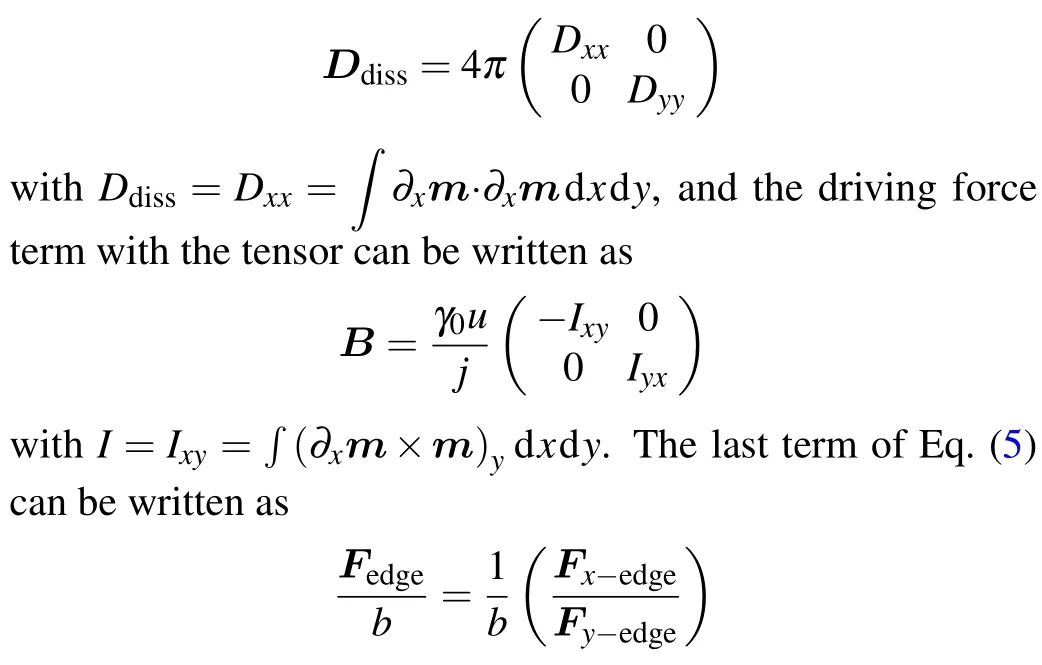
Fig.1. Schematic diagram of the antiferromagnetically exchange-coupled bilayer system and the proposed structure of logic gates. (a) The antiferromagnetically-coupled bilayer structure for the motion of a bilayer-skyrmion driven by the spin current,where we apply electric current in the HM layer to produce a vertical spin current to the magnetic layer; (b)the illustration of skyrmion logic AND and logic OR gates with two inputs and two outputs;(c)the illustration of skyrmion logic XOR and logic NOR gates with two inputs and one output;(d)the illustration of skyrmion logic NAND gate with two inputs and one output;(e)the illustration of skyrmion logic NOT gate with one input and one output.
3. Results and discussion
3.1. Realization of OR and AND logic functions
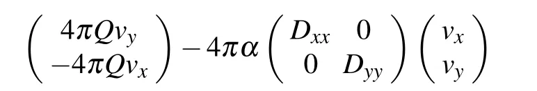
The proposed structure of the logic OR gate is shown in Fig. 1(b), input A and input B are placed on the left side of the nanotrack and the output C is placed on the upper right side as well as a triangular notch on the right side of the nanotrack.Here,the presence of a skyrmion represents the data bit“1”and the absence of a skyrmion represents the data bit“0”.When no skyrmion is created at inputs A and C, the logical operations OR“0+0=0”can be implemented. As shown in Fig. 2(a) and supplementary video S1, the generated isolated skyrmion at the input A moves along the+xdirection due to the spin torque and deviates to the-ydirection, and finally stops at the output C because of the notch boundary repulsion.Similarly, when a nucleated skyrmion at the input B moves along the nanotrack,it stops at the same site as the right region,as suggested by Fig.2(b)and supplementary video S2. Thus,the logical operations OR “1+0=1” and “0+1=1” can be implemented successfully. However,when both skyrmions from input A and input B move in this nanotrack as shown in Fig. 2(c) and supplementary video S3, the bottom skyrmion created at input B can stop at the lower side of the right region once it meets with the top skyrmion. As a result, the logical operation OR“1+1=1”can be implemented.
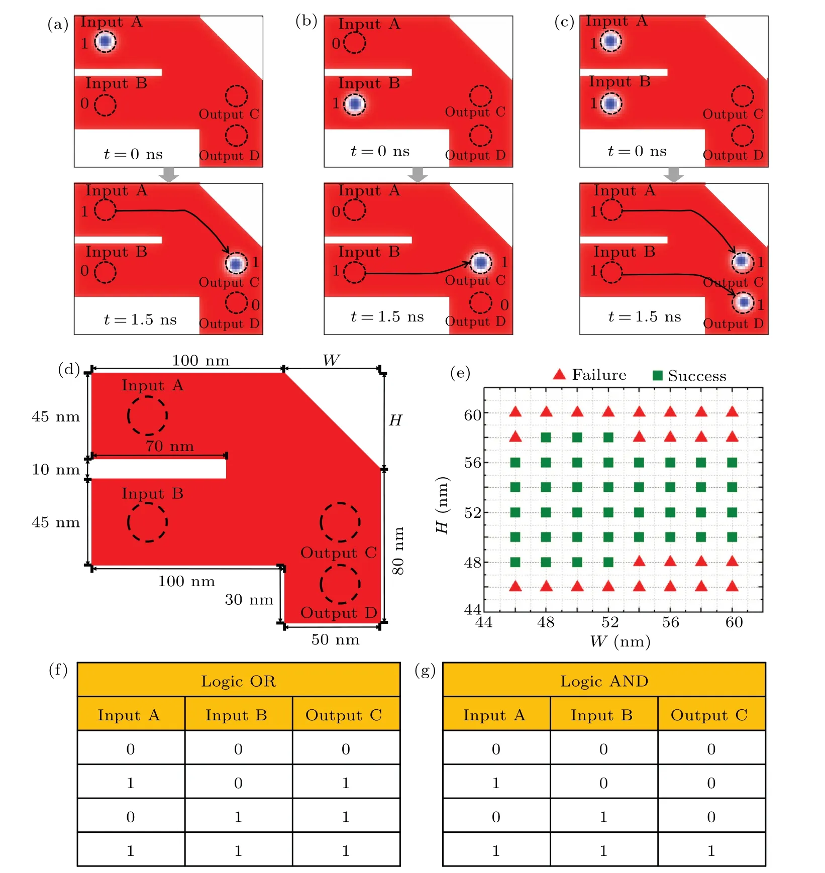
Fig.2. The micromagnetic simulations for the logic AND and OR gates in the SAF nanotrack. (a)–(c)The micromagnetic simulations of three cases for the logic AND and OR gates in the SAF nanotrack. (d)The top view of the logic OR and AND structure,where the black dashed circles represent the input and output MTJs. (e)The working window of the notch size in the logic AND and OR structure. (f)–(g)The truth tables for logic OR and AND gates.
The logic function of AND can be implemented in the same structure as the OR logic gate by changing the detection region as depicted in Fig.1(b). When the lower right region is set as the output D, the logic function “1·0=0” and“0·1=0”of AND are similar to the function of the OR gate which can be implemented as depicted in Figs.2(a)–2(b)and supplementary videos S1 and S2. In this structure,regardless of whether the isolated skyrmion is at input A or input B, it cannot reach input D under+xdirection driving current. Only when two skyrmions move along the+xdirection from input A and input B simultaneously,the bottom skyrmion nucleated at the input B can be squeezed into the output D region due to the skyrmion–skyrmion interaction as shown in Fig. 2(c)and supplementary video S3. Namely, the logical operation AND“1·1=1”can be implemented. It is noted that when no skyrmion exists for both inputs, there is no data transmission on the nanotrack and the logical operation AND “0·0=0”is achieved. Here, the height (H) and the base (W) length of the triangle influence the final stable position of the bottom skyrmion as shown in the top-view of the structure(Fig.2(d)),where the phase diagram of logical operations and the working window of the input position of AND and OR gates are provided in Fig. 2(e) and video S6(a). The corresponding truth tables for the logic OR and AND gates are shown in Figs.2(f)and 2(g).
3.2. Realization of XOR and NOR logic functions
The SAF bilayer XOR and NOR gates can be achieved with a structure similar to the AND gate as shown in Fig.1(c),input A and input B are at the left side of the F-type nanotrack,while output C is at the center of the right side. The difference between logic XOR and OR gates is that they lack the triangular notch in the upper right. In this regime,when no skyrmion is created in the inputs A and B, the logic operation of XOR gate“0⊕0=0”can be realized. As shown in Figs.3(a)–3(b)and supplementary videos S4 and S5, only one skyrmion is created in input A or input B. The skyrmion is driven by the spin current and then stops at the center of the right side due to the skyrmion–edge repulsion. Thus, the logic operation of XOR gate “1⊕0=1” and “0⊕1=1” can be implemented.However,when two skyrmions are created in inputs A and B,the two skyrmion driven by the spin current will push one another away from the center of the right nanotrack and output data bit“0”as shown in Fig.3(c)and supplementary video S6.In addition,the working window of the input position of XOR gate is given in video S6(a). So, the logic operation of XOR gate“1⊕1=0”can also be implemented.
The SAF bilayer NOR logic gate is proposed with the same structure as the XOR gate. Initially, a skyrmion is already nucleated at the output C. In this regime, as shown in Fig. 3(d) and supplementary video S7, when no skyrmion is created in the input A and B, the skyrmion in the center of the right side of the nanotrack remains stationary and the logic operation of the NOR gate=1”can be realized. However,when an individual skyrmion is created at the input A or B,driving by the +xdirection current, the left skyrmion will meet with the right one and push one another away from the center of the right nanotrack due to the skyrmion–skyrmion repulsion. Therefore, the logic operation of NOR “=”and “=” can be implemented as shown in Figs. 3(e)–3(f)and supplementary videos S8 and S9. Furthermore,if two skyrmions are nucleated in input A and input B,the skyrmion in output C will be annihilated by the repulsion between the skyrmions, and the two skyrmions created from the left side are going to push one another away from the center of the right region as shown in Fig.3(g)and supplementary video S10. In addition, the working window of the input position of NOR gate is given in video S6(a).Namely,the operation of the NOR gate“=0”can be realized.
Fig.3. The micromagnetic simulations and truth tables for the logic XOR and NOR gates in the SAF nanotrack. (a)–(c) Three cases of inputs and their corresponding micromagnetic simulations for the logic XOR gate in the nanotrack. (d)–(g) Four cases of inputs and their corresponding micromagnetic simulations for the NOR gate in the nanotrack. (h)The truth tables of the logic XOR and NOR gates.
3.3. Realization of NAND logic function
The logic function of NAND can be implemented in the proposed structure as shown in Fig.1(d). Here shows a triangular notch is on the lower right side and a trapezoidal notch is on the upper right side. Input A and B are placed on the left side of the nanotrack,while the output C is placed at the center of the right side. Similar to the logic NOR gate,there is an individual skyrmion at the center of the right-side nanotrack initially as shown in Fig. 4(a) and supplementary video S11.When both inputs data bit are“0”,there is no skyrmion moving in the SAF nanotrack and output“1”state and the logical operation of NAND“=1”can be implemented.As shown in Figs. 4(b)–4(c) and supplementary videos S12 and S13,considering only one skyrmion is created at the left input A or B,the left skyrmion will annihilate as it moves along the nanotrack at the boundary due to edge geometry confined. Hence,the operation of“=1”,and“=1”can be carried out.The most important operation of“=0”is implemented by the presence of skyrmions in both input A and B.As shown in Fig. 4(d) and supplementary video S14, all skyrmions in this operation will annihilate due to the skyrmion–skyrmion repulsion and skyrmion–edge repulsion. Here, the height (H) and the base(W)length of the triangle influence the state of the left skyrmion as shown in the top-view of the structure(Fig.4(e)).In addition,the phase diagram of the operations,the working window of the input position of NAND gate and corresponding truth tables for NAND gates are given in Figs. 4(f)–4(g)and video S6(b).
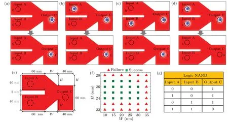
Fig.4. The simulation results of logic NAND gate with two notches. (a)–(d) The micromagnetic simulations of four cases of inputs for the logic NAND gate in the SAF nanotrack. (e)The top view of the logic NAND structure. (f)The working window of the notch size in the logic NAND structure. (g)The truth table of the logic NAND.
3.4. Realization of NOT logic function
The logic NOT gate is implemented in ay-junction structure as shown in Fig. 1(e). There are two nanotracks, where the input terminal A is at the left nanotrack and the output terminal B is at the center of the right nanotrack.Note an isolated skyrmion is initially nucleated in the center of the right nanotrack, as shown in Fig. 5(a) and supplementary video S15.When no skyrmion is created in the left nanotrack,namely input data bit “0”, the skyrmion in the center of the nanotrack remains at its original position due to the edge-skyrmion repulsion and output data bit“1”. Hence,the NOT gate“¯0=1”is accomplished. A skyrmion is created in the left nanotrack and driven by a+xdirection spin current. In that case,the left skyrmion will meet the right skyrmion and rotate at an angle of 90°and push one another away from the center of the right nanotrack as shown in Fig.5(b)and supplementary video S16.And the working window of the input position of NOT gate is also given in video S6(c). Therefore, the logic function of NOT gate“¯1=0”has also been implemented.
In particular, a logic switching delay is determined by the skyrmion velocity and the distance between the input and output terminals.[45,49]Therefore, the trade-off between skyrmion-based logic gates’ response speed and energy consumption needs to be considered.[48]Namely, a smaller driving current can decrease the energy consumption and a large current can be adopted for high switching speed. As shown in Fig. 6(a), the driving current of the above logic gates should be limited to 1×10¹¹A·m2–4×10¹¹A·m2,and SAF skyrmion velocity is proportional to the driving current density, where the larger current density may lead to SAF skyrmion annihilation at the right side due to large spin orbit torque. Figure 6(b)shows that the magnetic material parameters such asKandDcan also affect the skyrmion velocity, where the velocity increases asDincreases and decreases asKincreases in the above logic gates. Moreover,the skyrmion size can effectively reduce the scale of the logic devices and influence the distance between the input and output terminal,which can be determined by magnetic material parameters such as PMA and DMI constants. Figure 6(c) shows that the diameter of the skyrmion increases asDincreases and decreases asKincreases. Hence,the switching delay can be affected by downscale of the logic gates via adjusting magnetic parameters.

Fig.5. The simulation results of logic NOT gate. (a)The logical operation of NOT gate ¯0=1 on SAF nanotrack. (b) The logical operation of NOT gate ¯1=0 on SAF nanotrack.

Fig.6. Skyrmion velocity and skyrmion size vary with the current density and material parameters. (a)Simulation results of the motion velocity of isolated skyrmion vary with the current density. (b)Simulation results of the motion velocity with the PMA constant(K)and DMI constant(D). (c)The skyrmion diameter varies with PMA constant(K)and DMI constant(D).
4. Conclusion
In conclusion,we theoretically study the skyrmion velocity in the SAF monolayer, which indicates that the skyrmion velocity can be influenced by the driving force and the edge of the nanotrack. The theoretical results are consistent with the numerical simulation results. By designing geometric notches and tilted edges on the SAF nanotracks,we have proposed six basic logic gates based on the motion of SAF skyrmion, including the logic AND, OR, NOR, XOR, NOT, and NAND gates,which are implemented by spin–orbit torque,skyrmion Hall effect, skyrmion–skyrmion repulsion, and skyrmion–edge interaction. The proposed SAF skyrmion-based logic gates in this work have potential application in the future topological magnetic devices.
Data availability statement
The data that support the findings of this study are openly available in Science Data Bank at the following link http://doi.org/10.57760/sciencedb.j00113.00066.
Acknowledgements
Guoping Zhao acknowledges the support from the National Natural Science Foundation of China (Grant Nos. 51771127, 52171188, and 52111530143) and the Central Government Funds of Guiding Local Scientific and Technological Development for Sichuan Province, China(Grant No. 2021ZYD0025). Jing Xia was a JSPS International Research Fellow supported by JSPS KAKENHI(Grant No.JP22F22061). Yan Zhou acknowledges the support from Guangdong Basic and Applied Basic Research Foundation(Grant No. 2021B1515120047), Guangdong Special Support Project (Grant No. 2019BT02X030), Shenzhen Fundamental Research Fund(Grant No.JCYJ20210324120213037),Shenzhen Peacock Group Plan (No. KQTD20180413181702403),Pearl River Recruitment Program of Talents (Grant No.2017GC010293),and the National Natural Science Foundation of China (Grant Nos. 11974298 and 61961136006).Xiaoxi Liu acknowledges the support from the Grantsin-Aid Scientific Research from JSPS KAKENHI (Grant Nos.JP20F20363,JP21H01364,and JP21K18872).
猜你喜欢
现代经济信息(2022年35期)2023-01-11
科技创新与应用(2022年27期)2022-10-02
吉林广播电视大学学报(2021年4期)2022-01-14
华人时刊(2021年17期)2021-12-02
作文成功之路·小学版(2020年5期)2020-06-11
小天使·一年级语数英综合(2018年11期)2018-11-23
中低纬山地气象(2018年4期)2018-08-24
新高考·英语进阶(高二高三)(2018年8期)2018-01-15
资源再生(2017年3期)2017-06-01
低碳世界(2016年24期)2016-12-28
- Chinese Physics B的其它文章
- The coupled deep neural networks for coupling of the Stokes and Darcy–Forchheimer problems
- Anomalous diffusion in branched elliptical structure
- Inhibitory effect induced by fractional Gaussian noise in neuronal system
- Enhancement of electron–positron pairs in combined potential wells with linear chirp frequency
- Enhancement of charging performance of quantum battery via quantum coherence of bath
- Improving the teleportation of quantum Fisher information under non-Markovian environment