
Diamond/c-BN van der Waals heterostructure with modulated electronic structures
2023-09-05 08:48SuNaJia贾素娜GaoXianLi李高贤NanGao高楠ShaoHengCheng成绍恒andHongDongLi李红东
Chinese Physics B 2023年7期
Su-Na Jia(贾素娜), Gao-Xian Li(李高贤), Nan Gao(高楠),2,†,Shao-Heng Cheng(成绍恒),2,‡, and Hong-Dong Li(李红东),2,§
1State Key Laboratory of Superhard Materials,College of Physics,Jilin University,Changchun 130012,China
2Shenzhen Research Institute,Jilin University,Shenzhen 518057,China
Keywords: diamond,cubic boron nitride,heterointerface,first principles calculation
1.Introduction
As an ultra-wide band gap semiconductor, diamond has attracted considerable research interest as a favorable candidate for high-temperature and high-power electronic devices,due to the outstanding physical and chemical properties,such as high carrier mobility, high thermal conductivity, high break down electric field, exceptional hardness, and chemical stability.[1,2]The cubic boron nitride(c-BN)is the second hardest material,and it has been widely used as a coating material.Also, it is potential to apply c-BN to future electronic devices,due to its excellent electron transport properties and a variety of material parameters.[3]
The lattice mismatch between diamond and c-BN is only 1.36%.[4]It has been reported that c-BN is epitaxially grown on single-crystal diamond substrate by using ion beam assisted molecular beam epitaxy,[5–7]on seed crystals of diamond by a temperature gradient method,[8]and on polycrystalline diamond via plasma-enhanced chemical vapor deposition method.[9,10]Several theoretical studies of diamond/c-BN heterostructures with interfacial chemical bonds have been performed.[11,12]As is well known, the reconstruction or functionalization in diamond is essential for stabilizing the structures.[13]The H-terminated diamond samples are generally obtained in hydrogen plasma environment through the chemical vapor deposition method,[14]and the c-BN films could be treated by microwave hydrogen-plasma to obtain the hydrogenated c-BN surfaces.[15]Thus, it is naturally speculated that the c-BN would grow on the H-terminated diamond surface.The experimental and theoretical researches have found that constructing van der Waals heterostructures would purposefully get the novel properties, and the intrinsic properties are mostly preserved.[16–19]Meanwhile,the van der Waals integration offers an alternative bond-free integration strategy for building heterostructures without lattice and processing limitations.[20]However, the related researches about diamond/c-BN heterostructures with weak van der Waals interactions at the interface have not been reported.
In this work, we systematically investigate the structures and electronic properties of (100), (110), and (111)diamond/c-BN van der Waals heterointerfaces.Unlike the indirect and wide bandgaps for both bulk diamond and c-BN,all the heterostructures are direct bandgap semiconductors.
2.Computational method
The structural optimizations and electronic properties were calculated by using the density functional theory(DFT) implemented in the Vienerab initiosimulation package (VASP).[21,22]The exchange–correlation potential was Perdew–Burke–Ernzerh (PBE) within the generalized gradient approximation (GGA).[23]The projector augmented wave (PAW) method was used to describe the electron–ion interactions.[24]As shown in Fig.S1 in supporting information,the plane wave energy was selected as 600 eV after convergence test.Thek-point grids were 5×5×1 and 10×10×1 in geometrical optimizations and electronic properties calculations,respectively.Geometrical optimizations were finished by using the conjugate gradient method,until the energy convergence tolerance was less than 10−5eV and the force was less than 0.03 eV/˚A.A large vacuum of 30 ˚A was used to eliminate interactions between periodic images.
3.Results and discussion
The optimized structures of (100), (110), and (111)diamond/c-BN heterointerfaces are presented in Fig.1.For the bulk diamond surface and c-BN(100)surface,the stable structures have the dimers,[25]then we build(100)diamond/c-BN heterointerfaces with interface B–B and N–N dimers, which are defined as(100)-I structure and(100)-II structure,respectively.For(110)diamond/c-BN heterostructure,one structure is built, which is named (110)-I structure.The (1×1) and(2×1)reconstructed surfaces are possible for diamond(111)surface,[26]then we consider four(111)diamond/c-BN structures, designated as (111)-I to (111)-IV structures.Thus, in this work, seven kinds of diamond/c-BN heterostructures are considered,and the diamond and c-BN surface atoms are saturated by H atoms.Based on previous results,[27,28]the 9-layer thick diamond(100)and c-BN(111)slabs are used for building the models.The layer thickness of diamond (110), (111)slabs and c-BN(100),(110)slabs are chosen based on the test results in Fig.S2 in supporting information.
When a slab model is used to study the polar semiconductor surfaces,the charge transfer and interaction would appear between the two surfaces through the slab,which results in the irrelevant surface states in band structures.[29]To avoid the problem, Shirashi proposed a new slab model, in which fictitious H atoms were introduced to passivate the surface atoms.[30]Therefore, in this work, the B and N atoms on c-BN surfaces are saturated by the fractionally charged H atoms.Based on a simple chemical consideration of a covalent bond,the charge of virtual H atoms is set to 1.25e(0.75e) for the B(N)dangling bonds of the c-BN(111)[28]surface and(110)surface.For c-BN(100)structure with reconstruct dimers,the surface B–B(N–N)bonds are terminated with 1.5e(0.5e)of virtual H atoms.[25,31]
For the (100)-I ((100)-II)) structure, the B–B and N–N bond length in dimers are 1.742 ˚A (1.741 ˚A) and 1.572 ˚A(1.573 ˚A), respectively, which are close to those in hydrogenated c-BN(100)surface(1.75 ˚A and 1.58 ˚A).[25]The C–C bond length in dimer for diamond is 1.619 ˚A,approaching to previous results(1.61 ˚A).[26,32]The B–H(N–H)bond lengths of (111)-I, (111)-II, (111)-III, (111)-IV structures are 1.204,1.201, 1.204, and 1.198 ˚A (1.056, 1.056, 1.056, 1.057 ˚A),which are similar to those of c-BN (111) structures reported previously.[28]The interface distance between diamond and c-BN for the heterostructures are 1.915, 1.958, 2.093, 1.902,1.949,1.796,and 1.797 ˚A,respectively.
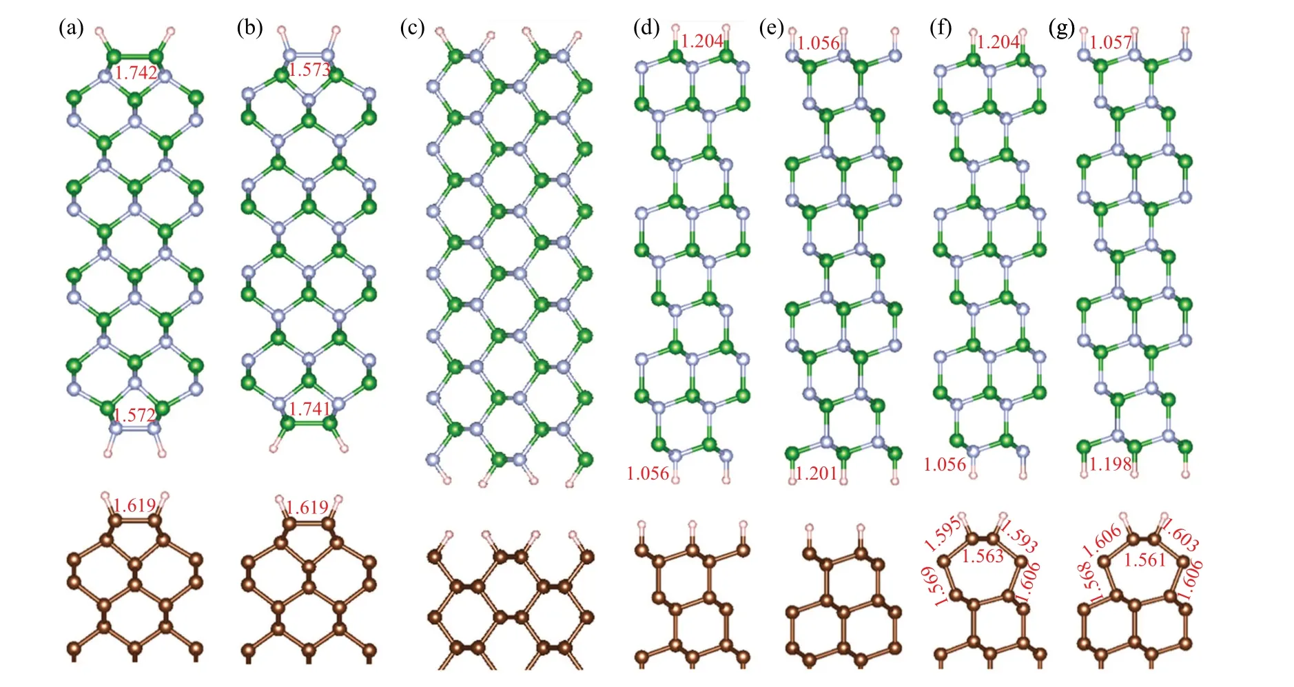
Fig.1.Side views of diamond/c-BN heterostructures for (a) (100)-I, (b) (100)-II, (c) (110)-I, (d) (111)-I, (e) (111)-II, (f) (111)-III, and (g)(111)-IV structures,with partial surface bond lengths marked and brown,green,grey,and pink balls denoting C,B,N,and H atoms,respectively.
The stability of the heterointerfaces is evaluated by the interface binding energy(γint)from the following formula:[17,33]
whereEdiamond,Ec-BN, andEdiamond/c-BN are the total energy of diamond, c-BN surface, and diamond/c-BN heterostructures, respectively, andSis the area of the interface between diamond and c-BN.The corresponding interface binding energy values for the heterostructures are 60.40, 60.46, 26.55,48.60,41.60,43.64,and 58.76 meV/˚A2,respectively.The order of interface binding energy values for diamond/c-BN heterostructures is (100)> (111)> (110).We suggest that the diamond(100)surface is a promising plane for c-BN growth.The large interface distance and moderate interface binding energy suggest the weak physisorption interactions between diamond and c-BN interface,which is consistent with the fact that both diamond and c-BN surfaces are fully functionalized with H atoms.
The band structures in Fig.2 show that the diamond/c-BN structures are direct band gap semiconductors with both valence band maximum (VBM) and conduction band minimum(CBM)at theΓpoint, which is different from the indirect bandgap for bulk diamond and c-BN.The band gap values of (100)-I, (100)-II, (110)-I, (111)-I, (111)-II, (111)-III,and(111)-IV structures are 2.948,2.660,2.078,2.731,0.922,2.872,and 0.647 eV,respectively,which are much smaller than those for bulk diamond and c-BN.Thus, the band gaps are modulated by heterostructure constructing.Apparently, there is no major difference between the electronic band structures of (100)-I, (100)-II, (110)-I, (111)-I, and (111)-III structures.While the band structures of(111)-II and(111)-IV structures are similar.
To analyze the electronic properties more clearly,density of states (DOS) for diamond/c-BN heterostructures is shown in Fig.3.The CBM of the (100)-I, (100)-II, (111)-II, and(111)-IV structures are contributed by c-BN, while the CBM of the(110)-I,(111)-I,and(111)-III structures are contributed by both the c-BN and diamond.For the VBM of the(100)-I,(100)-II,(110)-I,(111)-II,and(111)-IV structures,the contribution is mainly from the diamond part.While the VBMs of the(111)-I and(111)-III structures are mainly contributed by the c-BN part.The DOS features are similar for the (100)-I and (100)-II, (111)-I and (111)-III, (111)-II and (111)-IV structures.
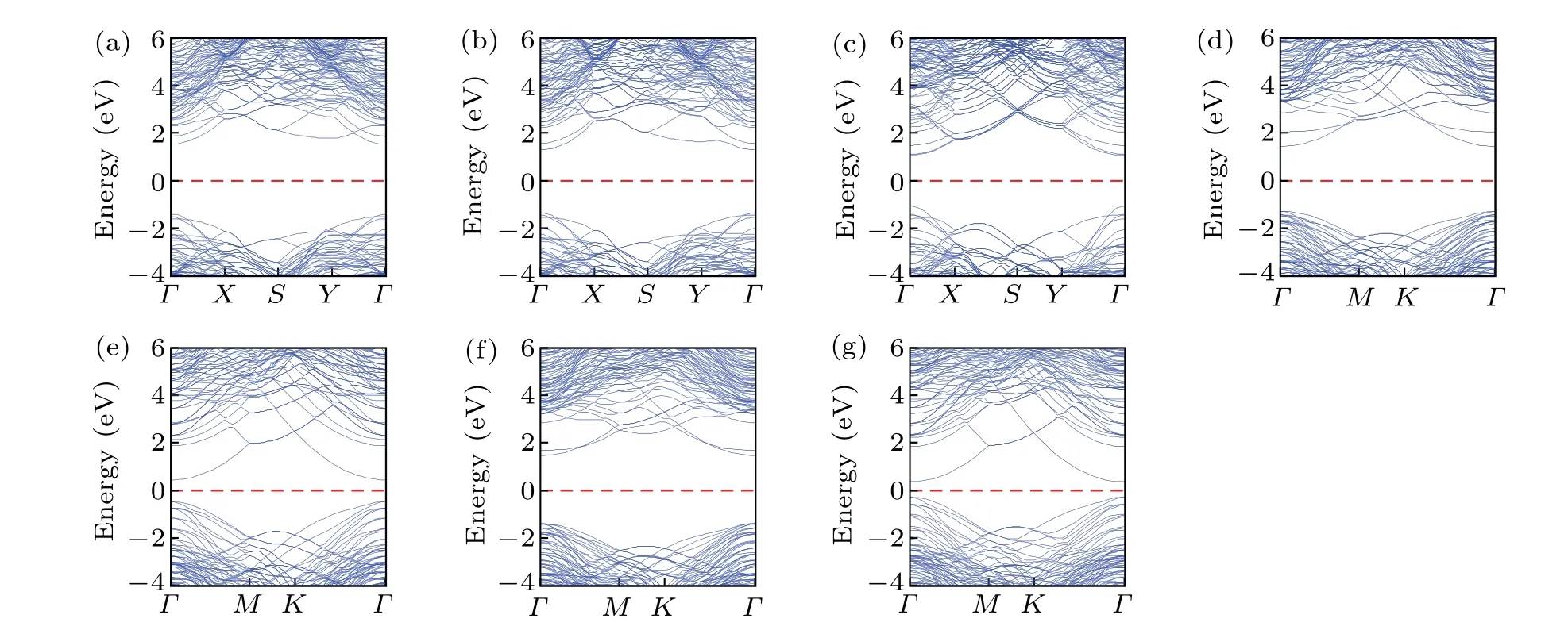
Fig.2.Band structures of diamond/c-BN heterostructures for (a) (100)-I, (b) (100)-II, (c) (110)-I, (d) (111)-I, (e) (111)-II, (f) (111)-III, (g)(111)-IV structures,with the Fermi energy setting to zero.
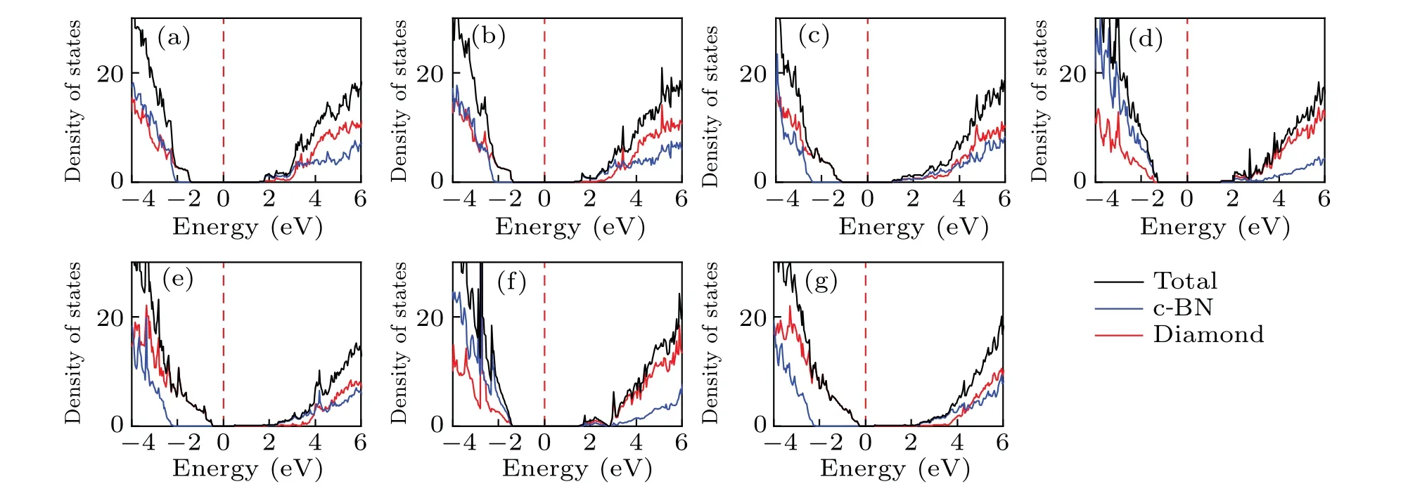
Fig.3.The density of states (DOS) of diamond/c-BN heterostructures for (a) (100)-I, (b) (100)-II, (c) (110)-I, (d) (111)-I, (e) (111)-II, (f)(111)-III,and(g)(111)-IV structures,with the Fermi energy setting to zero.
The differences in charge density between the diamond/c-BN heterostructures are presented in Fig.4.The charge density difference ∆ρis defined as ∆ρ=ρdiamond/c-BN−ρdiamond−ρBN(ρdiamond/c-BN,ρdiamond, andρc-BN are the charge densities of diamond/c-BN heterostructure,isolated diamond,and c-BN,respectively),to visualize the electron redistribution upon formation of heterointerface.We find the evident charge redistribution at the interface between the diamond and c-BN.The electron depletion is shown in diamond surface for(100)-I,(111)-I,and(111)-III structures, and electrons are accumulated in diamond surface for(100)-II,(111)-II,and(111)-IV structures.It is consistent with the Bader charge analysis that the electrons of 0.013,0.004 and 0.016eare transferred from diamond surface to c-BN for(100)-I,(111)-I, and(111)-III structures, and electrons of 0.012, 0.009, and 0.004eare obtained in diamond surface for (100)-II, (111)-II, and (111)-IV structures.It is caused by the electronegativity relation of B Fig.4.Charge density difference of diamond/c-BN heterostructures for(a)(100)-I,(b)(100)-II,(c)(110)-I,(d)(111)-I,(e)(111)-II,(f)(111)-III,(g)(111)-IV structures,with yellow(cyan)color representing electron accumulation(depletion),and isosurface value being 5.277×10⁻⁶ e/˚A3. In summary,we systematically investigated the interface structures and electronic properties of(100),(110),and(111)diamond/c-BN heterointerfaces by first principles calculation.According to the interface distance and interface binding energy, the interaction between diamond and c-BN is weak van der Waals force, which is consistent with the fact that the atoms in both diamond surface and c-BN surface are fully saturated by H atoms.The heterostructures show that the characteristics of the direct band gap with the band gap values of 0.647 eV–2.948 eV are different from those of the indirect and wide band gaps for bulk diamond and c-BN.The charge redistribution is found at the interface between diamond and c-BN.The electronic states can be manipulated for advanced electronic device applications. Acknowledgements Computation was carried out at the High-Performance Computing Center of Jilin University. Project supported by the Key-Area Research and Development Program of Guangdong Province, China (Grant No.2020B0101690001) and the National Natural Science Foundation of China(Grant Nos.51972135 and 52172044).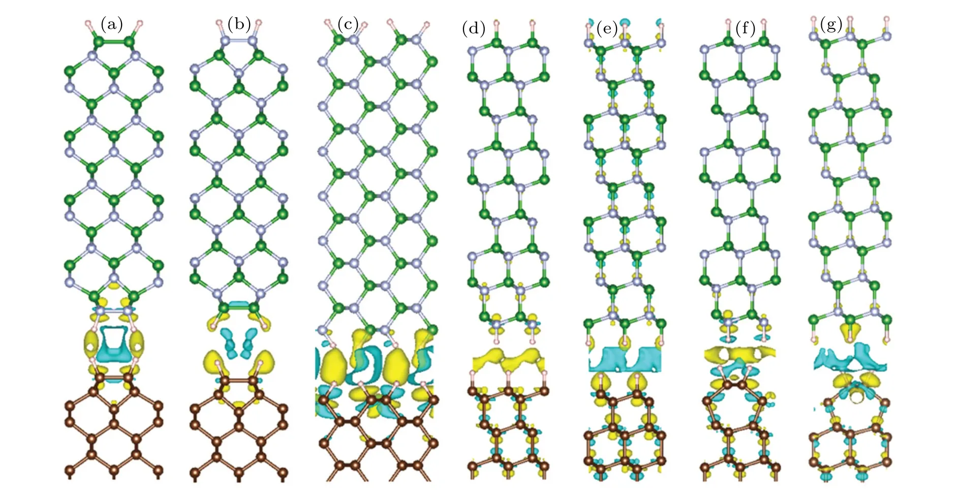
4.Conclusions
- Chinese Physics B的其它文章
- Interaction solutions and localized waves to the(2+1)-dimensional Hirota–Satsuma–Ito equation with variable coefficient
- Soliton propagation for a coupled Schr¨odinger equation describing Rossby waves
- Angle robust transmitted plasmonic colors with different surroundings utilizing localized surface plasmon resonance
- Rapid stabilization of stochastic quantum systems in a unified framework
- An improved ISR-WV rumor propagation model based on multichannels with time delay and pulse vaccination
- Quantum homomorphic broadcast multi-signature based on homomorphic aggregation