
Design optimization of a silicon-germanium heterojunction negative capacitance gate-all-around tunneling field effect transistor based on a simulation study
2023-10-11 07:56WeijieWei魏伟杰Weifeng吕伟锋YingHan韩颖CaiyunZhang张彩云andDengkeChen谌登科
Chinese Physics B 2023年9期
Weijie Wei(魏伟杰), Weifeng Lü(吕伟锋), Ying Han(韩颖), Caiyun Zhang(张彩云), and Dengke Chen(谌登科)
School of Microelectronics,Hangzhou Dianzi University,Hangzhou 310018,China
Keywords: negative capacitance (NC), gate-all-around (GAA), silicon-germanium heterojunction, gate-tosource overlap(SOL)
1.Introduction
Currently, reducing the power consumption of complementary metal–oxide semiconductor (CMOS) integrated circuits is an urgent problem that needs to be solved.One way to achieve this is to design CMOS devices with good switching characteristics that are defined by sub-threshold swing (SS).[1]TheSSof a conventional metal–oxide–semiconductor field-effect transistor (MOSFET) cannot be lower than 60 mV/decade due to the Boltzmann limit defined by its conduction mechanism.[2,3]A negative capacitance field-effect transistor (NCFET) can meet this requirement because of the negative capacitance(NC)effect of ferroelectric materials.[4]Due to the NC effect,an NCFET can amplify the surface potential of the channel to increase the channel current.[5]Another promising solution to the aforementioned problem could be to use a tunneling field-effect transistor(TFET),which generates the current by injecting charge carriers from the source into the channel via band-to-band tunneling.[6]TFETs can easily obtain a sub-60 mV/decadeSS.However, the TFETs have a low off-state current (IOFF)and on-state current (ION), which results in poor driving capability.[7]To overcome this limitation,materials with a narrow band gap and high carrier mobility, such as germanium(Ge) and indium arsenide (InAs), could be used to form a heterojunction.A heterojunction can improve the band-toband tunneling rate, thus increasing the channel current.[8,9]For sub-3-nm node devices,replacing the fin-type field-effect transistor with a gate-all-around (GAA) structure can further suppress the short-channel effect because of the improved gate control ability.[10–12]
In previous studies, NCGAA-TFETs were created by connecting a ferroelectric capacitor in series with a metal gate of a GAA-TFET.[13,14]Similarly, other studies used MATLAB simulations to combine the Landau–Khalatnikov equation with a GAA-TFET device model.[15]These techniques make the NCGAA-TFET ideal because they cannot reflect the ferroelectric material deposition on the oxide layer well.In addition, while depositing several materials between the oxide layer and the gate metal can improve device performance,it can also increase the fabrication complexity.[16]Furthermore,the vertical tunneling rate and tunneling area of an NCTFET can be improved by partially moving the gate to the source,thus increasing the channel current.[17–20]In addition,the gate-to-drain extension can improve the bipolar effect of a double-gate tunneling field-effect transistor.[21]Moreover,the inner gate, outer gate, and gate–source overlap can be used to improve the electrical performance of a device, but this makes its structure complex.[22]Moreover,applying the gatesource overlap to a line TFET can also improve the analog performance.[23]However, many of the TFET structures designed to enhance the channel current use compounds in heterojunctions,which increase the CMOS process complexity.
In this work,a GAA-TFET is combined with the NC effect, silicon–germanium (SiGe) heterojunction, and gate-tosource overlap(SOL),and a comprehensive investigation and analysis are conducted on the proposed NCGAA-SOL-TFET structure.The proposed structure can effectively increase the driving current and improve electrical performance.In addition,the electrical performance of the device can be easily optimized by adjusting the SOL length(LSOL)and the thickness of the ferroelectric layer(TFE).
2.Proposed structure design and simulations
A schematic of an NCGAA-SOL-TFET is presented in Fig.1(a), where the thicknesses of HfO2(TOX) and the ferroelectric layer (TFE) are 1 nm and 4 nm, respectively; the channel length(LG)is 15 nm;the source length(LS)and drain length(LD)are 20 nm;the radii(R)of the source,channel,and drain are 5 nm; and the gate-to-source overlap length (LSOL)is 3 nm.The GAA-TFET is selected as a baseline device and used for performance comparison; its schematic is presented in Fig.1(b).Germanium with a band gap of 0.66 eV is used as the source material,and silicon with a band gap of 1.12 eV is used as the construction material of the channel and drain;thus, a heterojunction is formed between the source and the channel.The doping concentrations of the source, channel,and drain are 1×1020cm-3,1×1015cm-3,and 2×1019cm-3,respectively.The device structural parameters and process parameters are in accordance with the IRDS More Moore 2021 version for a 3-nm node.[24]

Fig.1.(a) The NCGAA-SOL-TFET with SiGe heterojunction, SOL,and ferroelectric layer;(b)the GAA-TFET as a baseline device.

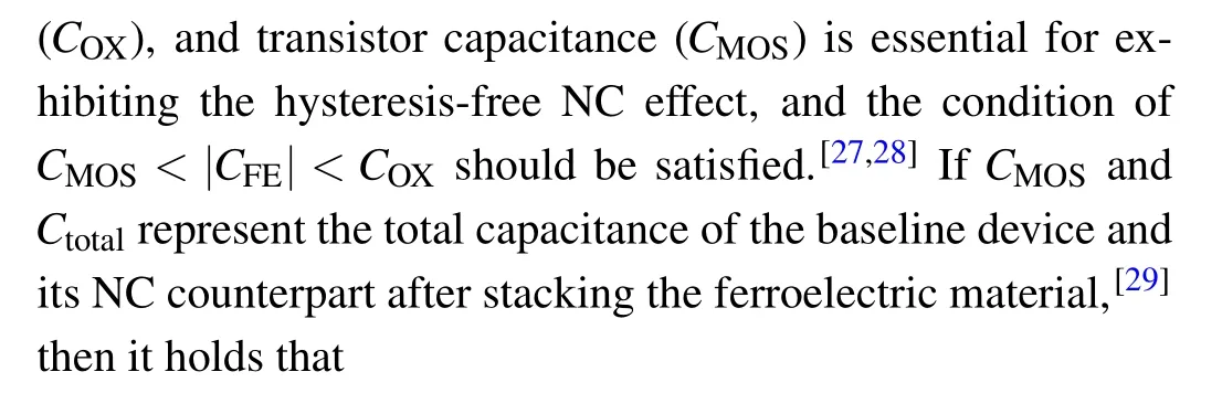
Excellent capacitance matching can be achieved whenCtotal≫CMOS, and this condition should be considered in device design and optimization.As shown in Fig.2,Ctotalis larger thanCMOS,and peak capacitance occurs at a smallerVGS.This indicates that the ferroelectric layer has exhibited a hysteresis-free NC effect.However,whenVGSis larger thanVDS,Ctotalis less thanCMOS,indicating that the capacitanceCFEdoes not matchCMOS.
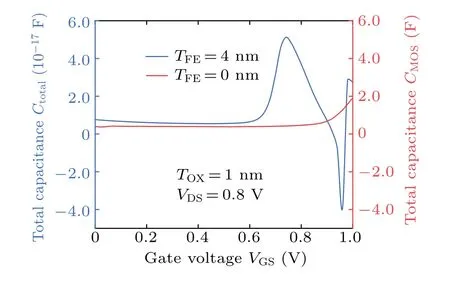
Fig.2.The total capacitance for TFE=4 nm and TFE=0 at TOX=1 nm.
The channel current in the TFET is mostly generated by the band-to-band tunneling of carriers,which mainly occurs at the heterojunction formed at the interface between the source and the channel.When the conduction band in the channel is lower than the valence band in the source, the probability of carrier tunneling is increased.Thus, carrier tunneling mainly occurs in the region between the valence band of the source and the conduction band of the channel.Under the condition of a uniform electric field,GBTBTdenotes the band-to-band tunneling rate of the carrier, which is derived from the Kane model[30,31]as follows:
whereAk,Bk, andθare the tunneling parameters of the material;AkandBkare 4×1014cm-3·s-1and 1.9×10⁷V/cm for silicon and 9.1×1016cm-3·s-1and 4.9×10⁶V/cm for germanium, respectively;Eis the electric field intensity under the current tunnel volume; andEgis the band gap.In the technology computer-aided design (TCAD) simulations,the Fermi–Dirac distribution model is used for a high doping concentration, and the hydrodynamic model is employed for nanodevices.The other models used in the TCAD simulations include the carrier high electric field velocity saturation model, the scattering model, the band gap narrowing model under high doping concentration,the SRH recombination model,the Auger recombination model,and the Landau–Khalatnikov ferroelectric equation.In addition, the nonlocal band-to-band tunneling model is used to judge the tunneling area based on the local variation in the energy band.The application of the listed physical models makes simulations conducted in this study more accurate and reliable.In addition,as shown in Fig.3,the simulated transfer characteristics(IDS–VGScurve) of the GAA-TFET are calibrated using previous experimental data.[32]
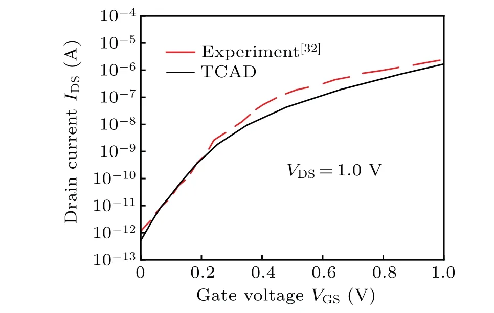
Fig.3.Calibration of the IDS–VGS curve using the experimental data.
3.Results,analysis and discussion
3.1.Source overlap effect on device performance
The energy band diagrams of the GAA-TFET in the off state (VGS=0,VDS=0.8 V) are presented in Fig.4(a).In this state,the valence band of the source is lower than the conduction band of the channel.Therefore,the band-to-band tunneling rate is low, and only a few electrons will tunnel into the channel to form the off-state current (IOFF).The energy band in the on state (VGS=1.0 V,VDS=0.8 V), where the valence band of the source is higher than the conduction band of the channel, is presented in Fig.4(b).Thus, a large number of electrons will tunnel into the channel to form the onstate current (ION).The transfer characteristics of the GAASOL-TFET are presented in Fig.5(a), where it can be seen that whenLSOLincreases,IONalso increases.WhenLSOLis larger than 1 nm, the sub-threshold current of the GAASOL-TFET is smaller than that of its GAA-TFET counterpart.However,asLSOLincreases,the increase in the saturation current is reduced.Furthermore, when the gate extends toward the source, the electric field on the left side of the heterojunction increases, as shown in Fig.5(b).Moreover, the energy bands of the source–channel interface and the left side of the source–channel interface bend,which improves the bandto-band tunneling area and tunneling rate, increasing the current.WhenLSOLincreases to 5 nm,the current almost reaches the saturation level.As shown in Fig.6, with the increases inLSOL, the electric field is mainly concentrated on the gate corner edge,which decreases the electric field intensity at the heterojunction center.As a result, the tunneling area and the area of the region with a high tunneling rate stop increasing whenLSOL>5 nm.The band-to-band tunneling generation rate and tunneling area along the central section of the GAASOL-TFET are presented in Fig.7.As shown in Fig.7,due to the effect of the electric field edge, whenLSOLincreases, the area with a high band-to-band tunneling rate is gradually concentrated on the heterojunction surface.This reduces the bandto-band tunneling rate at the heterojunction center so that the channel current stops increasing gradually.In addition, with the energy band bending on the left side of the source–channel interface,the width of the depletion region of the heterojunction increases, thus increasing the total capacitance (CMOS),as shown in Fig.8.The tunneling junction is equivalent to a reverse-biased diode.When the gate voltage is large enough,a large number of carriers will accumulate in the channel,and theCMOSwill be dominated by these carriers.However, the carriers that dominate the current are those that tunnel from the source to the channel.[9]
Fig.4.Band diagrams of the GAA-TFET and GAA-SOL-TFET:(a)off state;(b)on state.

Fig.5.(a)Transfer characteristics of the GAA-SOL-TFET at different LSOL values; (b)variations in the electric field intensity of the GAASOL-TFET at different LSOL values.
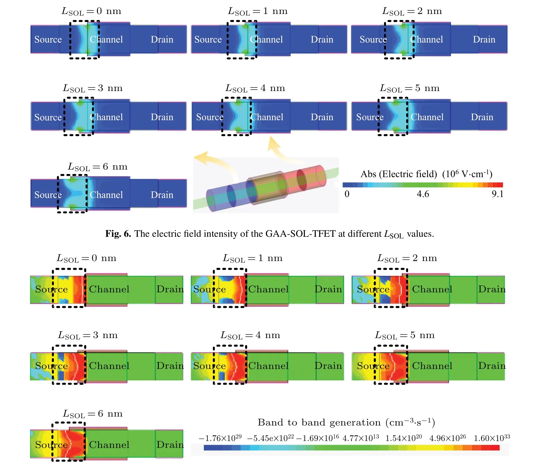
Fig.7.The band-to-band generation tunneling and tunneling area of the GAA-SOL-TFET at different LSOL values.
Therefore,CMOSand channel current are not dominated by the same group of carriers, which is the main difference between the TFET and the MOSFET.As shown in Fig.9,whenLSOLincreases, although theSSof the device gradually increases,it still remains below 60 mV/decade.A steeperIDS–VGScurve indicates a faster device switching speed,indicating a smallerSS.In Fig.5(a), it can be observed that theIDS–VGScurves atLSOL=1 nm andLSOL=2 nm are steeper than that ofLSOL=0.However, atLSOL>2 nm, theIDS–VGScurve becomes flatter than that atLSOL=0.Therefore,atLSOL=1 nm andLSOL=2 nm, theSSis smaller than atLSOL=0, but it becomes larger whenLSOL>2 nm.In addition,the threshold voltage(Vth)increases whenLSOLis less than 4 nm but decreases whenLSOLis larger than 4 nm while still staying lower than that of the baseline device.ConsideringVth,ION/IOFF, andSS, the GAA-SOL-TFET achieves its optimal performance atLSOL=3 nm.

Fig.8.The total capacitance of the GAA-SOL-TFET versus LSOL.

Fig.9.The SS value versus LSOL value; when LSOL increases, the SS of the GAA-SOL-TFET increases but remains below 60 mV/decade.The Vth of the GAA-SOL-TFET fluctuates in a small range as LSOL increases.
3.2.NCGAA-SOL-TFET design optimization
The variations in the channel surface potential at differentTFEvalues are presented in Fig.10.As shown in Fig.10,the surface potential in the NCGAA-SOL-TFET channel is amplified compared to that of the GAA-SOL-TFET.[33]The total capacitance increases due to the increase inLSOL, which makes the capacitance-matching process more complex.As presented in Fig.10,the potential amplification of the channel surface is almost the same atTFE<4 nm.This indicates that in the NCGAA-SOL-TFET,a largerTFEamplifies the channel surface potential obviously.
TheIDS–VGScurves of the NCGAA-SOL-TFET at differentTFEvalues are presented in Fig.11(a).As shown in Fig.11(a), in the subthreshold region, theIOFFgradually improves with the increase inTFE,except forTFE=1 nm.However, asTFEincreases, the variation trend of the saturation current becomes non-monotonic withVGSwhenVGS>VDS.WhenTFE<3 nm, the saturation current increases slightly withVGS, while it decreases atTFE=5 nm.AtTFE=4 nm,the saturation current increases monotonically and obviously.The main reason for this can be found using Fig.11(b)and formula(1).WhenVGSis small,the change ofCtotalatTFE=1 nm fluctuates, indicating that the capacitance matching becomes poor.WhenVGSis larger thanVDS, atTFE>2 nm, theCtotalof the NCGAA-SOL-TFET is smaller than that of the GAATFET,which indicates poor capacitance matching.As shown in Fig.12(a),for the NCGAA-SOL-TFET,the changes in theSSandVthvalues show opposite trends whenTFEincreases;namely,theSSfirst decreases and then increases,whereas theVthfirst increases and then decreases.The reason for this change can be observed in Fig.11(a).The results indicate that theIDS–VGScurve is the steepest atTFE=0, so theSSis the smallest atTFE=0.Moreover, theIDS–VGScurves atTFE=1 nm andTFE=5 nm are almost the flattest among all the curves.

Fig.10.Variations in channel surface potential in the NCGAA-SOLTFET under different TFE values.
As shown in Fig.12(b), bothIONand the peaktransconductance of the NCGAA-SOL-TFET are improved compared to the other devices,and the peak-transconductance appears at a lower gate voltage.The electrical characteristics in Table 1 show thatIONand the peak-transconductance of the NCGAA-SOL-TFET are 2.32 times and 2.11 times larger than those of the other devices,respectively.In addition,Vthdrops from 0.39 V to 0.31 V.It should be noted that both the NC effect and the SOL can enhance the driving capability,but theSSof the NCGAA-SOL-TFET is slightly larger than that of the GAA-TFET, resulting in a reducedION/IOFF.Therefore,different optimized designs should be used for different performance requirements.The GAA-SOL-TFET is suitable for devices with good switching performance,whereas the NCGAASOL-TFET is suitable for devices with a high driving current and a low threshold voltage.
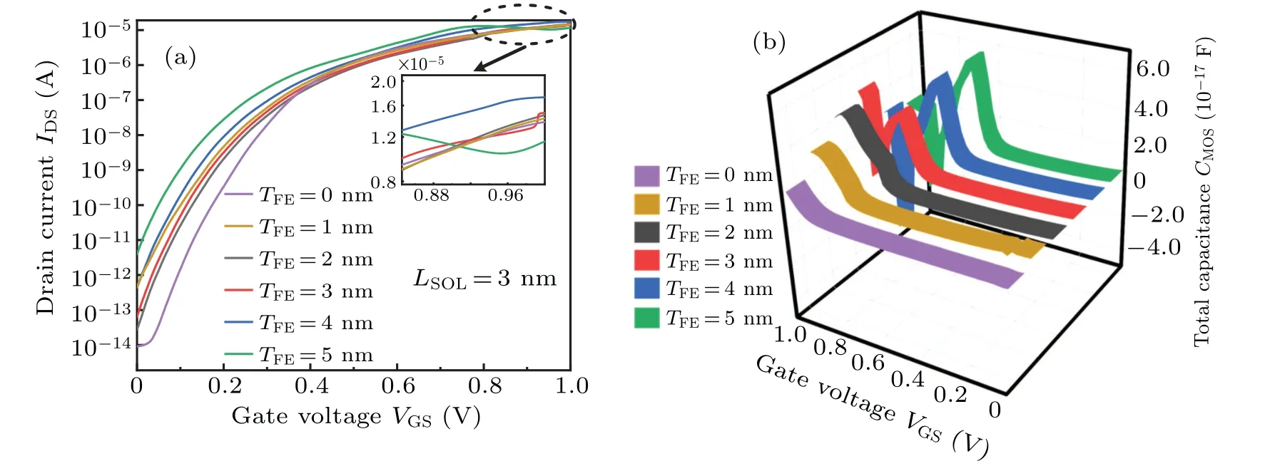
Fig.11.(a)The IDS of the NCGAA-SOL-TFET versus VGS under different TFE values;(b)Ctotal–VGS characteristics of the NCGAA-SOL-TFET at LSOL of 3 nm and TFE of 0,1 nm,2 nm,3 nm,4 nm,and 5 nm.
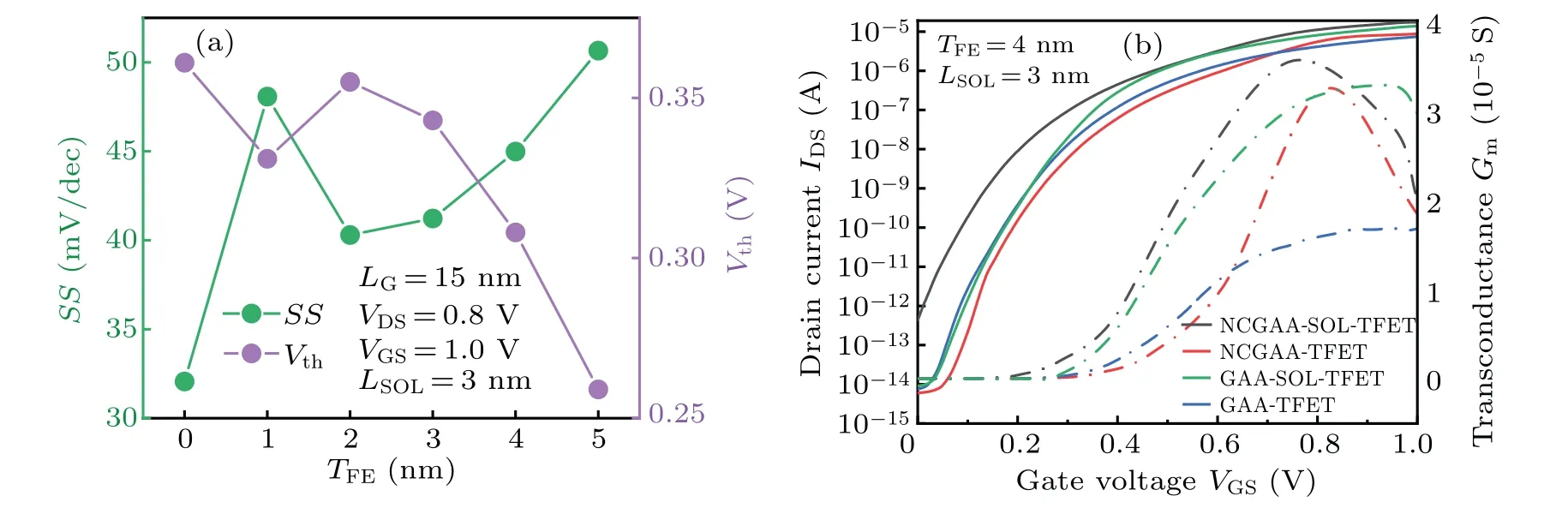
Fig.12.(a)Changing trends of the SS and Vth at different TFE values;(b)IDS–VGS and Gm–VGS curves of the GAA-TFET,GAA-SOL-TFET,NCGAA-TFET,and NCGAA-SOL-TFET.

Table 1.Electrical performance comparison results of different devices.
4.Conclusion
This study proposes the NCGAA-SOL-TFET structure and performs a comprehensive investigation of the proposed structure via TCAD simulations.The results indicate that the NC effect on the silicon–germanium heterojunction and the gate-to-source overlap increase the band-to-band tunneling rate and tunneling area of the source–channel interface,increasing the device current.Thus,in the proposed structure,the problem of the insufficient driving capability of the TFET is effectively solved.In the NCGAA-SOL-TFET structure,changing the gate-to-source overlap length will affect the NC matching and dynamic response characteristics.Therefore,the SOL length and the ferroelectric layer thickness should be considered in the device design.In addition, the proposed structure can improve the driving ability of the GAA-TFET by design optimization.However,the improvement in driving ability may be at the cost of sub-threshold leakage, although the sub-threshold swing of the NCGAA-SOL-TFET is still less than 60 mV/decade.In summary,the proposed NCGAASOL-TFET can achieve both high driving ability and low subthreshold swing,which makes it suitable for future low-power circuit applications.
Acknowledgements
The research presented in this work was supported by the Zhejiang Provincial Natural Science Foundation of China(Grant No.LY22F040001), the National Natural Science Foundation of China(Grant No.62071160),and the Graduate Scientific Research Foundation of Hangzhou Dianzi University.
猜你喜欢
大众文艺(2022年19期)2022-10-19
运动精品(2022年1期)2022-04-29
小猕猴智力画刊(2022年3期)2022-03-29
Chinese Physics B(2022年3期)2022-03-12
香格里拉(2021年2期)2021-07-28
海峡姐妹(2020年5期)2020-06-22
启迪与智慧·上旬刊(2019年11期)2019-09-10
民族音乐(2019年3期)2019-08-14
钟山风雨(2018年4期)2018-11-12
宝藏(2017年7期)2017-08-09

- Chinese Physics B的其它文章
- Dynamic responses of an energy harvesting system based on piezoelectric and electromagnetic mechanisms under colored noise
- Intervention against information diffusion in static and temporal coupling networks
- Turing pattern selection for a plant–wrack model with cross-diffusion
- Quantum correlation enhanced bound of the information exclusion principle
- Floquet dynamical quantum phase transitions in transverse XY spin chains under periodic kickings
- Generalized uncertainty principle from long-range kernel effects:The case of the Hawking black hole temperature