
Design,fabrication and optimization of electromagnetic absorption metamaterials
2023-10-11 07:55QiLou娄琦XuDongZhang张旭东andMingGangXia夏明岗
Chinese Physics B 2023年9期
Qi Lou(娄琦), Xu-Dong Zhang(张旭东), and Ming-Gang Xia(夏明岗),2,3,†
1Department of Applied Physics,School of Physics,Xi’an Jiaotong University,Xi’an 710049,China
2MOE Key Laboratory for Nonequilibrium Synthesis and Modulation of Condensed Matter,School of Physics,Xi’an Jiaotong University,Xi’an 710049,China
3Shaanxi Province Key Laboratory of Quantum Information and Optoelectronic Quantum Devices,School of Physics,Xi’an Jiaotong University,Xi’an 710049,China
Keywords: metamaterial,electromagnetic wave absorption,fractal design
1.Introduction
1.1.Electromagnetic waves and electromagnetic absorbing materials
Nowadays, a sharp increase in electromagnetic radiation is generated by various electronic products in the process of use due to the development of science and technology.The immune,cardiovascular and central nervous systems are only a few of the body’s systems that are damaged to a certain extent by electromagnetic radiation.Currently, electromagnetic interference(EMI)shielding and absorption technologies can effectively stop the leakage of electromagnetic radiation.For EMI shielding materials,absorption and reflection significantly contribute to the total EMI shielding efficiency.However,the reflected waves cannot be eliminated and can still adversely affect other electronic components inside the precision electronic instruments.The ideal material for attenuating electromagnetic waves should be absorption-based.Accordingly,the application of high-performance electromagnetic absorption materials is a superior way to neutralize harmful electromagnetic radiation by attenuating electromagnetic waves and converting them into thermal energy.[1]To protect human beings from electromagnetic pollution and equipment from downtime due to electromagnetic waves, considerable effort has been exerted to synthesize high-performance microwaveabsorbing materials.In addition, military radar technology has made sufficient progress in recent years that the military industry has an increasing need for electromagnetic shielding and stealth coatings for vehicles, ships and aircraft to effectively reduce the radar reflection cross-section (RCS) of weaponry and improve its survivability on the battlefield.[2–6]Given the exceptional application scenarios, microwave absorbing materials must feature more excellent properties(such as lightweight, chemical resistance and oxidation resistance)to meet the requirements of normal applications in harsh environments,thus posing a serious challenge to traditional microwave absorbing materials.For example, magnetic materials will demagnetize at a high temperature and lose their properties.Metal matrix composites are highly dense and unsuitable for use in high-temperature oxidation environments.Therefore,diversified electromagnetic metamaterial absorbers(EMMAs) and their design methods are urgently needed to cope with the demands of diverse and complex application scenarios.
Additionally, the constant development of industry and technology in today’s human society has produced and used an enormous amount of energy,much of which is lost in various ways.The focus has changed to EMMAs as a means of environmental protection,resource conservation and carbon emission reduction.Efficient electromagnetic absorbers can improve energy utilization and optimize material costs and adaptability to harsh environments for energy devices(e.g., photovoltaic devices and solar collectors).Conventional EMMAs have remarkable features in that the thickness of an electromagnetic wave absorber is almost of the same order of magnitude as its target wavelength,which will significantly increase its thickness if low-frequency band performance is desired.However, the rapid advances in nanofabrication technology and the introduction of the metamaterial concept in the past decades have opened a new gateway to the design of miniaturized and high-performance EMMAs.Metamaterials provide an ideal solution to the above-mentioned problems due to their excellent space-filling properties.
1.2.Introduction of metamaterials
Metamaterials are artificially designed media in which the subwavelength-sized metallic or dielectric unit cells are periodically and repeatedly arranged to display unique and exotic electromagnetic properties.This metamaterial absorber achieves the absorption, of electromagnetic waves through the resonance phenomena, with the top metasurface allowing the penetration of incident electromagnetic waves, the middle substrate capturing the radiation and the bottom layer blocking the transmission of electromagnetic waves.Metamaterials have a profound potential for optical imaging,[7]stealth,[2–6,8]antennas,[9–13]holography,[11,14]ultra-sensitive sensors,[15]filters,[16]photovoltaic solar cells,[17–19]and perfect absorbers.[20–30]EMMAs are highly sought after by researchers because of their extraordinary absorption properties.In particular,perfect absorption remains one of the interesting applications of EMMAs.
Metamaterial absorbers were experimentally demonstrated for the first time in 2008.[31]Thereafter, various metamaterial absorbers with different properties, such as single-band,[32–35]dual-band,[5,36]multiband,[12,37]and broadband,[28,38–46]absorbers have been extensively investigated (Fig.1).To date, several forms of metamaterial absorbers that are suitable for operation in the microwave, terahertz, visible and ultraviolet ranges have been reported (Table 1).The desired absorption performance can be achieved by tailoring and optimizing the geometrical parameters of the constituent primary cells.

Fig.1.Schematic of the introduction of EMMA, including features from design to application.
Wanget al.proposed a low density SiC aerogel EMMA.[52]This EMMA not only possesses the excellent mechanical properties of the precursor, but also shows the EAB of 5.5 GHz and the RLminof-15 dB.This work is novel,but the electromagnetic properties are not yet enough to meet the needs of applications such as electromagnetic stealth.Zhanget al.prepared a hollow EMMA based on CuS.[50]This work achieves lower reflection loss.Due to its good impedance matching performance and rich micro-interfaces,this EMMA shows excellent electromagnetic absorption performance.At 2.3 mm thickness of sample, EAB is 6.88 GHz, RLminis-40 dB.Zhanget al.designed a hybrid EMMA that achieved a significant increase in EAB while achieving a lower reflection loss,which is-48 GHz.[55]This EMMA is composed of traditional magnetic absorbing materials and graphene films to achieve an EAB of 30.5 GHz including ultra-low frequencies.This EMMA is characterized by low RLmin, high EAB, light design weight and robust environmental adaptability, which reflects its engineering value.
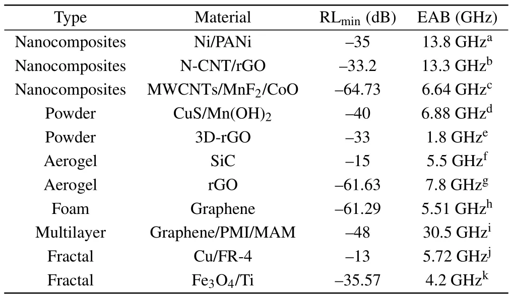
Table 1.Summary of the RLmin and effective absorption band (EAB)for different types of EMMA.
The structure of a metamaterial absorber can be modelled using inductance and capacitance.According to the transmission line theory,the metamaterial absorber can be considered an LC circuit.This LC equivalent circuit reduces the reflection coefficient and produces perfect absorption at the resonant frequency.Broadband absorption can be achieved by using several methods, such as nanocomposites, fractal structures and the installation of lumped elements(resistors)in fractal metamaterial structures, each of which has some advantages and disadvantages.Considering the cost and technical difficulty of these methods, the use of lumped elements is a cost-effective and relatively simple method.By choosing the appropriate resistor value, a certain degree of broadband absorption can be obtained.
1.3.Effective absorption structures: metal metasurface and films
Apart from the various applications of individual nanoparticles (NPs), the localization effect of the interacting nanoparticles on electromagnetic fields is more significant,expanding the use of NPs.An ensemble of NPs,whose distance from each other does not exceed the diameter of individual particles,can strongly trap incident light in the subwavelength range and create a huge localized field due to the surface plasmon.The spectrum of NPs is determined by the interaction between the individual localized surface plasmon resonances.The magnitude of the confined field and its frequency significantly depend on the shape, size and space between NPs.In the simple case, a conspicuous electric field response is generated when a metal particle or particles are located above a metal surface.Specifically, the interaction of the dipole with the induced image in the mirror also affects the resonance when it is located near the conducting layer (mirror), in addition to the dipole–dipole interaction.
Early dipole-conducting film structures consisted of metallic particles(dipoles)and metallic films(conducting surfaces).Interactions between the local surface plasma of the nanostructures and themselves led to remarkable absorption of electromagnetic waves.In the study of the effect of particle arrangement on optical properties, Papanikolaou found that silver spheres(90 nm in diameter)located on top of a silver film(40 nm thick)absorbed most incident electromagnetic waves,leading to the first theoretical report of a highly absorbing film-particle absorber.[58]
Patterned nanostructures are gradually replacing the earlier metal particles and broadening the application areas of dipole-conducting film structures due to the rapid development of wafer fabrication processes.Nicolaet al.[59]used a chemical vapor deposition(CVD)method to grow a single layer of monocrystalline graphene on a copper foil and subsequently transferred it to a substrate to prepare a broadband,highly efficient,tunable Sierpinski carpet-shaped photodetector.In this work,the authors show that an almost unity internal quantum efficiency can be obtained by a reasonable geometric design.However, the principle behind the above works is the same,and all of them design a three-layer structure with a top metasurface,a dielectric film and a substrate.The top metasurface with special properties often requires lithography, CVD and other processes to complete the fabrication.Some representative studies are listed in Table 2.
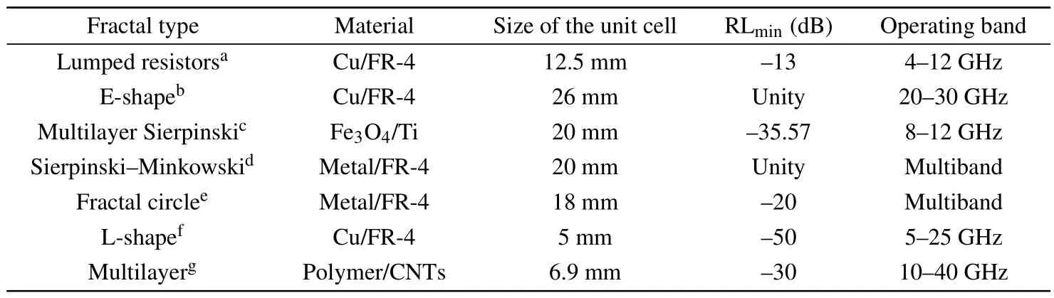
Table 2.Representative works of fractal EMMAs and their performance.
2.Theoretical preparation
2.1.Transmission line theory
When electromagnetic waves propagate to the surface of a loss-dispersive metal, transmission, reflection and absorption occur.The reflection of electromagnetic waves includes reflections that occur at interfaces and multiple reflections that occur between interfaces.In this case,multiple reflections result in a continuous path of electromagnetic wave propagation,enhancing the loss of electromagnetic waves.Electromagnetic waves lead to thermal effects in the material due to the interaction of electromagnetic fields with the electronic and molecular structure of the material,thereby converting the energy of electromagnetic waves into heat.This process is macroscopically manifested as the absorption of electromagnetic waves by the material and the phenomenon of self-generated heat.In the absorption–dissipation process,the microwave behavior of the material can be characterized by parameters, such as reflection coefficientR,specific reflection coefficient at isolated interfacesRM, reflection loss RL and the scattering parameterS11.These natural physical quantities can find their counterparts defined in transmission line theory,a well-established discipline in microwave engineering.The theory helps in understanding the mechanism of microwave absorption by materials and can be used to develop new materials that efficiently absorb microwaves.However,the maturity of the theory does not assure that it can be easily applied to materials because its focus needs to shift from circuit response to the intrinsic properties of the material.Specifically,transmission line theory cannot simply be applied to all materials or metamaterials without regard to their intrinsic properties.In reality,the nonhomogeneous microstructure or defects of the material will affect its microwave behavior to a certain extent, thus causing large or small deviations between the predictions of transmission line theory and experimental results.According to the transmission line theory,the impedance and reflection loss of a material can be calculated as follows:[65]
高校实验室既是实验教学的主要基地,也是学校科研和技术服务的主要场所,其中仪器设备是实验室的重要组成部分。机能实验中心有大量教学仪器,日常使用率较高,损坏率也较高。机能实验技术人员要改变传统的“传帮带”学习方式,更系统、全面、准确地学习实验仪器的操作和维护知识,提高对仪器故障的排查能力。把握仪器代理商对仪器定期检测的机会,积极请教实验设备工程师,认真听讲,做好笔记。实验技术人员有机会应该到相关企业、科研院所进行业务培训和学习交流[8]。此外,实验技术人员要灵活运用计算机系统进行仪器设备的管理和使用,提高实验室管理信息化水平,对实验资产状况能做到“及时记录、随时可查”的信息化统计[9]。
whereZ0is the impedance of free space,εris the relative complex permittivity(εr=ε′-jε′′),µris the relative complex permeability (µr=µ′-jµ′′), j is imaginary unit,cis the speed of light in a vacuum,fis the frequency of the incident electromagnetic wave,anddis the sample thickness of the material under test in the direction of microwave propagation.ε′andµ′represent the storage capacity of the material for electromagnetic wave energy,whilstε′′andµ′′represent the loss capacity of the material for electromagnetic wave energy.[66]This part of the loss is mainly caused by the dipolar,resonance and relaxation mechanisms in the material under the action of microwaves.[32]According to Eqs.(1) and (2), an ideal situation where ifεrandµrare numerically equal is not difficult to find,and a reflection of zero will be obtained.Even if equalεrandµrare difficult to obtain, as long as they are as close as possible, high electromagnetic wave absorption can be achieved.[67]
2.2.Fractal dimension
Metamaterial absorbers, which have been introduced in Section 1,have received a significant amount of attention from researchers because of their exotic and unique electromagnetic properties.An important approach to constructing metamaterial absorbers is the introduction of periodic fractal structures to obtain physicochemical properties that conventional materials do not possess.The fractal structure is similar in nature and can be divided into several parts,each of which is identical or similar to the whole when reduced.This structure appears as a rough and fragmented geometric structure with morphological features that fill the space with a non-integer number of dimensions.Fractal geometry needs to measure the complexity of many fractal structures with the same parameter.Hence,the fractal dimension is proposed to compare the complexity of two curves or surfaces.
From a computational point of view, fractal dimension has several definitions, including box dimension, Bouligand–Minkowski dimension, intersection dimension and Hausdorff dimension.Although they lead to different algorithms and results when they are discretized and applied to digitized data,most of these dimensions are equivalent in the continuous domain.Therefore,this review mainly adopts Hausdorff dimension to describe the complexity of fractals,which is commonly used by researchers.Take the classical fractal structure of the Sierpinski carpet as an example (Fig.2), this structure is designed starting from a square progenitor cell with side lengthL0.This structure is divided into 3×3 arrays of sub-cells with side lengthL1=L03-1, and the central sub-cell is replaced with the upper-level cell.More complex fractal structures of high fractal order can be obtained by iteratively generating sub-cells with edge lengthLt=L03-tin the same way.After each iteration, the size of the sub-cells is reduced by a fixed ratio(i.e.,ℒ=∋), and each unit cell generates the next level of unit cells by a fixed number (i.e.,N=∀).Accordingly,the Hausdorff dimension of the Sierpinski carpet can be calculated asdH=lgN/lgℒ=∞.∀∃.[9]The dimension of various other types of fractal structures can be given by the same calculation,and it is only required to find the scaling of adjacent level unit cells and the number of sub-cells generated by each unit cell.

Fig.2.Schematic diagram of the standard Sierpinski fractal of(a)firstorder,(b)second-order,(c)third-order.
2.3.Dielectric and ohmic losses
The calculation of the material impedance is introduced in Subsection 2.1.According to Eq.(1), that the minimum RL is obtained when its impedance and that of the free space satisfy the impedance matching condition.The impedance of a metamaterial absorber with a substrate (mirror) also corresponds to almost unity absorption.The energy of the absorbed electromagnetic waves is dissipated on the surface and inside the absorber and converted into thermal energy by two mechanisms: ohmic loss due to the metal resistance and dielectric loss due to the intermetallic substrate layer.[31]This process is macroscopically exhibited by the absorption of microwaves,which is converted into dissipated heat energy.

Fig.3.(a) Perspective, (b) front view, (c) end view of the proposed absorber.
Ohmic losses cause the temperature of the material through which the current flows to rise due to heat generation, so the magnitude of ohmic losses is mainly influenced by the intrinsic properties and geometrical characteristics of the metallic part of the metamaterial.Tuonget al.[68]used thin-plate resistors as the main loss medium for conductor–dielectric–conductor perfect absorbers (Fig.3), reducing the thickness of copper squares to a few nanometers.The experimental results show that the absorption at 16 GHz is 82.25%at a thickness of 50 nm.The optimal absorption is achieved when the thickness is 10 nm.Under this thickness, most of the energy of the incident electromagnetic wave is dissipated by the thin sheet resistance on the surface of the metamaterial.In fact,the energy loss is similar to the power distribution,which also indicates that the energy loss is realized by the heat production of the thin metal plate.Specifically,the ohmic loss plays a dominant role in perfect absorption.The impedance matching condition is also satisfied in this case (i.e., the effective surface impedance of the absorber at this frequency matches the free space impedanceZ0).[68]
The application of an electric field to a dielectric produces polarization.However, the polarization process is not instantaneous but lags behind the voltage;this lag is typically caused by the polarization of the dipole and space charge,and this process serves as dielectric relaxation.[68,69]Dielectric loss is the phenomenon of the dielectric itself heating up by consuming part of the electrical energy caused by the above-mentioned phenomenon in an alternating electric field.In the subsequent work of Tuonget al., a perfect absorption dominated by the dielectric loss was obtained by changing the properties of the insulating dielectric layer whilst retaining the originally obtained dimensional parameters.The best loss tangent was obtained at the resonant frequency.The simulation results show that most of the power distribution in the metamaterial is transferred from the metallic layer to the insulating dielectric,further demonstrating that the thermal effect of the material in this case is dominated by the dielectric loss.Similar EMMAs are shown in Fig.4.

Fig.4.Schematic diagram of first-order, second-order and third-order absorbers,(a)–(c)in Ref.[13],(d)–(f)in Ref.[60],(g)–(i)in Ref.[70].
3.Absorber design and fabrication
EMMA’s design boils down to the design of metamaterials, which usually start with microstructure.For fractal metamaterials, firstly, fractal geometric characteristics must be determined to obtain a fractal unit cell.Secondly, metasurface can be obtained by transformation, arrangement and combination of unit cells.Then,the metasurface is combined with the dielectric layer and the backplane to get the prototype of fractal EMMA.And the subsequent optimization is obtained by changing the geometric characteristics, material composition, physical properties and other means on this basis.For nanoparticle composite metamaterial absorbers and powder absorbers, the design generally starts from organic or inorganic materials with known wave absorbing properties.By changing material composition, compactness, preparation conditions, geometric parameters, etc., EAB broadening or RLmindecreasing can be realized,and finally the effective absorption of target band can be realized.
Given the special working characteristics of the electromagnetic absorbers, researchers want them to meet the requirements of different working scenarios in terms of the operating frequency range, absorption bandwidth, polarization independence, electromagnetic absorption capacity and adjustability.[15,71]To date, a wide variety of EMMAs have been reported, including fractal metamaterial absorbers, nanocomposite absorbers and powder material absorbers.Common fabrication methods have been developed for the structural and material characteristics of different absorbers.Metamaterial absorbers designed with fractal geometry concepts typically have highly designed periodic regular structures, which are difficult to spontaneously form in the raw material.Accordingly, standard lithography and electron beam lithography are frequently used to complete the preparation of the metasurface or unit cell arrays.By contrast,nanoparticle composite metamaterial absorbers and powder material absorbers are different.Firstly, both designs require metal nanoparticles or powders with a high fill in the substrate material to exploit the interaction of the local plasmon resonance of individual nanoparticles.Secondly, large area coverage is essential in most applications,[72–74]which precludes electron beam lithography and requires the self-organized formation of nanostructures.This condition explains why techniques, such as vapor deposition and magnetron sputtering,are popular for tailoring nanostructures and their properties.Both techniques allow good control of the filling of metal particles in the base material and the distribution of depth and the incorporation of metal nanoparticles with a well-defined composition.Given the high binding energy and low metalsubstrate interaction energy between metal atoms and clusters,metal nanoparticles are typically formed by self-organization during metal and component co-deposition.[49]Various types of absorbers have different material compositions,microstructures and absorption mechanisms.Therefore,absorbers differ in terms of absorption bandwidth and peak.
3.1.Fractal metamaterials
Nicolaet al.prepared a novel plasmonic multiband metamaterial based on Sierpinski carpet space-filling fractals in a step of electron beam lithography, evaporation and liftoff.In this work, Sierpinski carpets were patterned on CaF2and Si/SiO2substrates by electron beam lithography, and a 160 nm layer of 950 K poly methyl-methacrylate (PMMA A2 1:1, 1% in anisole) was deposited by spin coating on a substrate previously cleaned with O2plasma and dried on a hot plate at 180°C for 7 min.A 10 nm thick Al conductive layer was deposited on the CaF2substrates by thermal evaporation at a rate of 0.02 nm/s at a working pressure of 10-6mbar to prevent the charge accumulation caused by the electron beam.The conductive layers were washed in KOH(1 M) for 10 s and rinsed in deionized water.The layers were incubated in a low-temperature mixture of MIBK:IPA 1:3 for 30 s.A certain thickness of Ti/Au film was deposited by electron beam evaporation on the substrate at an operating pressure of 10-6mbar at a rate of 0.02 nm/s and finally lift off with hot acetone.The films were then characterized by scanning electron microscopy,surface-enhanced Raman spectroscopy analysis and optical microscopy.The results were in good agreement with the expected material parameters.Landyet al.adopted the same patterning, evaporation and stripping process to prepare the fractal metamaterial absorber.However,considering the minimum size of the pattern, the more efficient and less demanding experimental conditions of standard lithography were chosen in this work.Unlike electron beam lithography, standard lithography adopts UV light for exposure rather than an electron beam.Because of the shorter de Broglie wavelength of electrons,electron beam lithography allows to fabricate smaller-sized devices,whose machining precision can be no more than 100 nm.Unlike electron beam lithography,lithography requires the preparation of a mask for the determined pattern in advance to ensure accurate patterning during lithography.From the perspective of cost,lithography is usually a higher priority than electron beam lithography because of its high efficiency and low cost.
Nicolaet al.also prepared a gold/graphene plasma fractal absorber as shown in Fig.5(a), which achieves broadband, efficient, polarization-insensitive, and tunable light detection at room temperature mainly by depositing a patterned graphene array in a substrate,where the metal part can be patterned by the standard process of electron beam lithography,metal evaporation, and exfoliation as described above.[9]As a non-metallic material, graphene cannot be deposited on a pre-prepared substrate by evaporation and lift-off, so a different process from the preparation of fractal metal arrays is used to prepare patterned graphene in this work.Singlelayer monocrystalline graphene was grown by chemical vapor deposition (CVD) on copper foil using a tube furnace at 1060°C and 25 mbar.Graphene was transferred from copper to the target substrate using a semi-dry transfer method.The films were spin-coated with PMMA film and graphene was electrochemically exfoliated from the grown substrate in 1 M NaOH solution.The graphene/PMMA film was removed from the electrolyte, rinsed with deionized water, and dried under ambient conditions.The films were deposited on the target Si/SiO2substrate at 120°C, and the PMMA carrier polymer was removed in acetone to obtain the transferred monolayer single-crystal graphene.The gold patterning was essentially the same as the electron beam etching described above.Subsequent characterization was accomplished with a scanning electron microscope(SEM),atomic force microscope and surfaceenhanced Raman spectroscopy analysis.A similar process for the preparation and characterization of metamaterial absorbers is described in Ref.[59].

Fig.5.(a) The perspective of gold/graphene plasma fractal absorber in Ref.[9].(b)Electromagnetic absorption performance of EMMAs of different materials.
3.2.Nanoparticle composite metamaterial absorber
Polymer-based nanocomposites feature more complex microstructures, and suitable impedance-matching distributions and microstructures help in enhancing the dissipation of incident electromagnetic waves.Zhanget al.[54]precisely designed ultralight polyimide-based graphene foams with ordered layered structures by a bidirectional freezing process and performed controlled construction.The formation of more layered interfaces per unit volume of foam effectively promotes the layer-by-layer dissipation of vertically incident electromagnetic waves, resulting in efficient broadband electromagnetic absorption performance of the foam.In this work, the researchers propose a simple, low-cost and effective method to prepare ultralight polyimide-based graphene nanocomposite foams with ordered layered structures by a bidirectional freezing process.Water-soluble poly(amic acid)(PAA) as a precursor can be homogeneously compounded with graphene oxide (GO) in water and converted to polyimide after thermal imidization, resulting in composites with excellent mechanical strength and thermal stability.Compared with other 2D nanomaterials,the flexible GO nanosheets have a larger spreading ratio and play a more important auxiliary role in promoting the formation of ordered lamellar structures during the bidirectional freezing process.Moreover, these nanosheets can be used as a pore modifier to regulate the lamellar spacing between ordered skeletons.Moreover, reduced GO can be used as a functional material to promote the optimization of impedance-matching distribution.Accordingly, the effective construction of an ordered lamellar structure successfully gives polyimide/graphene foam ultralow density,excellent electromagnetic compatibility(low RL)and wide effective absorption bandwidth(EAB).Furthermore,the electromagnetic absorption performance also exhibits outstanding tunability by controlling the impedance distribution and microstructure of the backbone at different freezing temperatures and concentration ratios of PAA and GO.
This work used a modified Hummers method for the oxidation of graphite flakes.Water-soluble PAA was prepared by condensation reaction with equimolar ratios of PMDA and ODA with DMAc as the raw material.Then, PAA salt was prepared with TEA as a hydrophilic surface modifier.Then,the PAA was poured into deionized water and repeatedly washed to remove the solvent and unreacted raw materials.The water-soluble PAA was obtained after freeze-drying.GO(10 mg/mL)was uniformly mixed with PAA at a concentration ratio of 1:1, as shown in the flowchart (Fig.6(a)).The prepared GO/PAA pure sol was poured into a bidirectional freeze cast mold placed on a cold copper plate with 15°C wedge PDMS as a spacer and kept at 4°C for 24 h for sol–gel transition.The prepared GO/PAA hydrogels were further frozen at-70°C for 6 h and freeze-dried in a vacuum.The obtained GO/PAA foams were heated at 100°C,200°C and 300°C in a nitrogen stream for 1 h to reduce GO and imidise PAA,respectively.SEM,Fourier transform infrared spectroscopy,thermogravimetric analysis and vector network analyzer were subsequently used for the characterization to obtain the morphological features and electromagnetic parameters of the samples.
Liuet al.[38]synthesized a novel core–shell structure composite.The Co–C/void/Co9S8ternary composite consisting of porous carbon covered by Co nanoparticles as the core and Co9S8as the shell in the outer layer has shown excellent RL and absorption bandwidth in the experiments, which can be used for ultra-broadband and efficient low-frequency microwave absorption.The composites in this type of work are chemically synthesized, but the specific method of synthesis varies.Liuet al.synthesized ZIF/sulfide core–shell composites via anion exchange method.In Fig.6(b), 40 mg of ZIF powder was dispersed in 40 mL of ethanol under ultrasonic and magnetic stirring conditions.Then,0.18 g TAA was added to the suspension and kept at 60°C for 10 min,20 min,60 min and 120 min.The Co:S molar ratio was 1:2.4, and the corresponding samples were labelled as ZIF/S-2,ZIF/S-3,ZIF/S-4 and ZIF/S-5.Additionally, 40 mg ZIF powder was dispersed in 40 mL ethanol, and 90 mg TAA was added and kept at 60.The Co/S molar ratio was 1:2.2.The corresponding sample was labelled as ZIF/S-1.Finally,the above-mentioned precipitates were washed with ethanol and dried under a vacuum.The prepared pure ZIF and ZIF/sulfide powders were annealed at 600°C for 2 h under Ar atmosphere at a heating rate of 3°C/min to obtain Co–C, Co–C/Co9S8and Co9S8–CoS composites.Many similar composite synthesis methods can be found in the following works.[33,38,93,94]

Fig.6.(a) Schematic diagram of the preparation process of rGO/PI foam in Ref.[54].(b) Schematic diagram of Yolk-shell-structure Co–C/void/Co9S8 composites in Ref.[38].
3.3.Powder absorbers
Gaoet al.[95]prepared a ZnN4-based MOF-derived carbon composite.The theoretical calculations show that this significant enhancement comes from the coordination structure of individual Zn atoms in the carbon matrix,which is associated with a high density of permanent electric dipoles that act as atomic-scale polarization sites under alternating electromagnetic fields.This zinc single-atom microwave absorber(SAMWA)has a high Zn–N4content(18.4%)and defect density (2.43×1011cm-2), resulting in an appreciable dielectric loss tangent(~5.6).The preparation of SAMWA started with the synthesis of ZIF-8 by firstly mixing 3.16 mmol Zn(NO3)2–6H2O with 20 ml MeOH and 20 ml distilled water.Meanwhile, 24.4 mmol 2-methylimidazole (MeIM) was dissolved in 20 ml MeOH, and the methanolic solution of Zn(NO3)2–6H2O was poured into the methanolic solution of MeIM and stirred for 3 h.Finally, the solution was washed with MeOH several times,collected by centrifugation and dried at 110°C for 12 h to obtain ZIF-8 powder.Then,the solution was placed in the argon environment at different temperatures for 3 h to carbonize to obtain a series of SAMWA with different properties.
In contrast with the ‘bottom-up’ method of powder material preparation described above,Fanget al.[51]used a‘topdown’ method to prepare a powder material as the operating material for EMMAs.The authors prepared 3D-rGO powders by hydrothermal and thermal treatment methods.Firstly,200 mg of GO was dispersed in 100 ml of deionized water using ultrasound for 2 h.Then, the solution was transferred to a teflon-lined autoclave reactor.The reactor was heated to 180°C within 1 h and kept for 6 h to form 3D-rGO components.After the sample is cooled to room temperature, it is removed from the reactor and freeze-dried.Moisture in the 3D-GO assembly can be removed by freeze-drying.Next,the samples are transferred to an alumina crucible, loaded into a tube furnace filled with argon(Ar)and reduced with hydrogen(H2) at 900°C for 30 min.Finally, the 3D-rGO assemblies were ground into powder with a particle size of~100 μm.
RLminand EAB are two important indicators to measure EMMA’s performance.Researchers hope to fabricate EMMAs with low RLminand high EAB.This review summarizes some of the reported works that applied different materials and methods to get different RLminand EAB in Table 3.In Fig.5(b),the EAB of carbon-based composites and magnetic multicomponent EMMAs is ordinary, but the RLminis lower than that of other materials.Graphene aerogel/foam is capable to achieve ultra-wideband or ultra-low RL, whereas the preparation process is complex.Metal fractals and dielectric films’ and carbon nanotubes’ EAB and RL are generally inferior to other materials, but can also achieve broadband absorption through processing methods such as increasing thickness.Therefore, researchers can select appropriate materials to prepare EMMAs according to the requirements of absorption band and absorption capacity.

Table 3.Summary of different processing methods.
4.Optimization methods
We are interested in the specific properties of absorbers in different application scenarios.For example, radar stealth materials are of most interest for their broadband and efficient absorption capability in the radar wave band.Filters for a perfect absorption of specific frequencies are the most important properties, and photodetectors have higher requirements for the sensitivity of electromagnetic waves.Great efforts have been exerted by researchers for different usage requirements to improve the absorption,broaden the absorption spectrum or optimize the electromagnetic compatibility of metamaterials at low frequencies.
4.1.Improving absorption
High absorbance or low reflectance is the most important property of EMMAs,and several commonly used methods can effectively improve the absorbance of electromagnetic waves in specific frequency bands.For example, methods, such as improving the impedance matching conditions and changing the circuit load resistance, have been shown to greatly affect the microwave behavior of the material.
4.1.1.Impedance matching
The decisive role of impedance matching on the microwave response of an EMMA has been discussed from a theoretical point of view in Section 2 of this paper, which also provides an important idea to improve the electromagnetic compatibility of an EMMA (i.e., to improve the impedance matching condition to obtain a higher absorption).This idea is also supported by the following experimental results.Costanzoet al.[90]proposed a novel Minkowski fractal metamaterial absorber with the structure shown in Fig.7(a).To achieve near-unity absorption of electromagnetic waves at the operating frequency,the absorber should satisfy the following objectives: maximize the percentage of absorbed RF energy and ensure insensitivity to the polarization of the incident electromagnetic signal.This task also requires that the impedance of the absorber matches the impedance of the free space at the operating frequency to meet the prerequisites for perfect absorption.The calculation and simulation results show that the impedance matching is highest at the frequency of 2.45 GHz when the absorption of the EMMA also reaches near unity of 99%.At other frequencies,the impedance matching is worse than 2.45 GHz,and the absorption of the EMMA is lower than the peak of 99%.This finding also proves that the impedance matching case has the least reflection effect of the material on the electromagnetic wave, in other words, the lowest electromagnetic reflectance at this time(because the transmittance in this work is zero).Similar result can be found in Ref.[60].
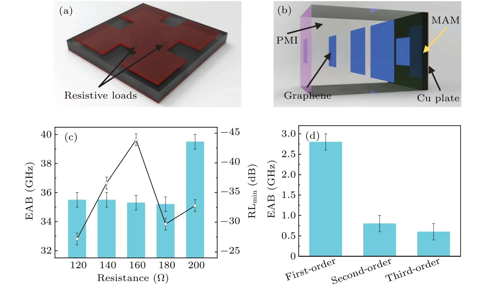
Fig.7.Schematic diagram of metamaterial absorber in(a)Ref.[90],(b)Ref.[55].(c)Variation of RL and EAB with resistance in Ref.[55].(d)Effect of different fractal levels on EAB in Ref.[60].
4.1.2.Adjusting the load resistance
Zhanget al.[55]proposed a hybrid metamaterial absorber consisting of a conventional magnetic absorbing material and a multilayer meta-structure pre-designed with a graphene film to achieve broadband and efficient absorption of electromagnetic waves using resonant mode coupling.The geometrical parameters of the metamaterial absorber are shown in Fig.7(b).A series of simulation experiments were designed to obtain the most favorable resistance of graphene(r1)for electromagnetic absorption.The value ofr1was varied from 120 Ω/m to 200 Ω/m with a variation of 20 Ω/m each time.The obtained RLminand EAB are shown in Fig.7(c).In this figure,the lowest reflectance of the absorber is obtained whenr1=160 Ω/m,which is the result the researchers wanted.However, the authors did not give much explanation for this phenomenon,pending subsequent investigations by the researchers.The available results already show that changes in the resistance in the material can affect the microwave behavior of the metamaterial absorber,which is also,in principle,a result triggered by changing the impedance.
4.2.Increasing EAB
Electromagnetic shielding and absorption are important potential applications for EMMAs.In fact, EMMAs can be applied in the fields of electromagnetic shielding and electromagnetic stealth.[3]Specific application scenarios dictate that such EMMAs should have broadband absorption characteristics(i.e.,they should be able to absorb electromagnetic waves of different frequency ranges with significant effects).However, ultra-wideband absorption is still extremely difficult to achieve because of the sensitivity of the dielectric and ohmic losses in materials to the frequency of incident electromagnetic waves.Many researchers have exerted plenty of efforts in this field.This work illustrates a few methods that can effectively broaden the absorption band.
4.2.1.Changing the fractal level
The size effect of the microwave behavior of a metasurface has been described in previous work[107,108](i.e.,an equal scaling up or down of the size of a metamaterial with the same material and geometry results in a change in its targeted absorption of electromagnetic wave frequencies).The fractal structure is similar in that each level of the fractal pattern is essentially an enlargement or reduction of the fractal pattern of the adjacent level.In combination with the aforementioned phenomena,we have reason to speculate that the introduction of one more level of fractal in the fractal hypersurface may produce a new characteristic absorption peak for a new frequency band.Related work has been reported on this conjecture.Bilalet al.studied a specially designed metallic Eshaped fractal-based perfect metamaterial absorber(PMA),as shown in Figs.4(d)–4(f),whose top surface consists of square fractal ring resonators surrounded by a special E-shaped fractal design.[60]
The researchers designed a series of experiments to investigate the effect of fractal order on the designed metamaterial absorbing properties (Table 4).Firstly, the design of the zero-order fractal was explored, and multiple absorption peaks were obtained.The square metal sheet was then replaced with an E-shaped resonant structure.The simulation results showed that the electromagnetic absorption performance of the absorber significantly changed.Some absorption peaks disappeared, some were retained, and some absorption peaks appeared that were not originally present.The same change occurred for the second-order fractal,where near-uniform absorption peaks still appeared at the impedance-matched frequencies.When an asymmetric metal ring is inserted in the center of the fractal geometry,the overall absorption spectrum of the absorber is broadened and responds differently to the TE and TM modes of the electromagnetic wave.This phenomenon arises because the addition of the asymmetric resonant ring breaks the quadruple symmetry of the original fractal structure.However,this aspect is not the focus of the study here,but the increase in the number of fractal stages essentially broadens the absorption spectrum of the fractal metamaterial absorber.

Table 4.EM absorption performance for different fractal levels.
4.2.2.Adjusting the composition
Zhanget al.[105]prepared a series of graphene foam materials with different chemical compositions and physical structures by using a simple and controllable chemical synthesis method and demonstrated that the graphene foams have good properties through an in-depth analysis of their composition,structure and electromagnetic absorption properties.In the experiments, the synthesized pristine graphene foams were placed under different temperature conditions for annealing to regulate the ratio of C, H and O elements in the materials.The RL of the graphene foam samples obtained at different annealing temperatures is shown in Fig.8(a).The original unannealed graphene foam(T0)has low C/O and poor absorption in the test band.The RL of T200 annealed at 200°C is not significantly different from that of T0.After the annealing temperature was increased to 400°C,the electromagnetic absorption performance of the graphene foam significantly improved.T400 had a minimum RL of-28.4 dB at 13.9 GHz and could reach a desirable-10 dB or less in the frequency range of 5.6–16.9 GHz.The results show that the T600 has the best electromagnetic absorption performance.In addition to the maximum RL of-34.0 dB at 13.1 GHz,the RL<-10 dB bandwidth reaches 14.3 GHz,accounting for 89.4%of the entire measured bandwidth.The changes in the electromagnetic absorption properties of the composites do not monotonically evolve as the annealing temperature continues to increase.By contrast, the EMC performance of the graphene foam starts to weaken when the temperature exceeds 600°C.Therefore,this work suggests the existence of an optimal annealing temperature in this case, such as 600°C, at which the elemental ratio of the material is most favorable to achieve broadband electromagnetic absorption.The same approach was used in Refs.[48,75,79]to broaden the EAB of the composites.
4.3.Methods for improving the low-frequency performance
Electromagnetic wave devices and devices operating in the low-frequency band have been widely used in wireless data communication systems, local area networks, household appliances and other fields.Studies have found that the widespread use of these devices can seriously harm human health by weakening the biological immune system, damaging DNA strands and inducing cancer.The key to solving this problem is to develop materials that can attenuate harmful electromagnetic wave pollution.However, not enough research has been conducted on low-frequency microwave absorption.The typical electromagnetic absorption devices have good absorption performance in the X–K band (8–27 GHz),whilst the response in the L–S (1–4 GHz) or even lower frequency band is relatively weak, making it difficult to achieve effective absorption.The researchers found that changing the chemical composition of the metamaterial absorber makes it difficult to shift the absorption peak across a large span toward the low-frequency band,but changing the geometry of the absorber can more effectively improve the low-frequency performance of the device.Zhanget al.[55]greatly improved the low-frequency electromagnetic absorption capability of the predesigned absorber by changing the thickness of the electromagnetic absorption layer.In Fig.8(b),the absorption peak of the absorber moves toward the lower frequency with the increase in d, and the maximum span even reaches more than 5 GHz.
Wanget al.[52]designed and prepared silicon carbide aerogels with ceramic properties and aerogel morphology to achieve broadband efficient electromagnetic absorption under extreme environments.The researchers firstly prepared the SiC aerogel by chemical synthesis and confirmed its composition and structural morphological characteristics by XRD,SEM, TEM and XPS characterization.The effect of different thicknesses of silicon carbide aerogel on RL was investigated in the experiment, as shown in Fig.8(c).The absorption peak of the silicon carbide aerogel gradually moves to the lower frequency direction with the increase in the sample thickness.The span of the absorption peak shift reaches more than 10 GHz.Similar work can be found in Refs.[93,94,110].All of the above-mentioned work demonstrates the significant contribution of material size to low-frequency absorption,but this also poses limitations for the application of low-frequency metamaterial absorbers(Table 5).Subsequent in-depth studies by researchers on miniaturization and lightweight are needed.

Fig.8.(a) Effect of annealing temperature on EAB and RL in Ref.[105].The frequencies corresponding to the low-frequency absorption peaks of absorbers of different thicknesses(b)in Ref.[55],(c)in Ref.[52].

Table 5.Methods for improving low-frequency absorption.
5.Conclusion and perspectives
The research on metamaterial perfect absorbers is still in its early stages.Complex structure,preparation difficulties and high cost limit the process of putting these absorbers into applications.More efforts must be exerted to bridge the gap between laboratory-scale fabrication and industrial applications.Nevertheless, the current theoretical and experimental results show the great potential of this new metamaterial for various applications.[112–115]
Photovoltaic and rectifier antennas are areas of interest as major uses of highly absorbing metamaterials.Recent work has realized novel broadband polarization and incidence angle insensitive metamaterial absorbers and their energy harvesting applications,namely,rectifier antennas and power harvesters.The authors demonstrate through numerical simulations that the absorption and energy conversion of electromagnetic waves in the specific frequency range of the environment by the circuit is achieved due to impedance matching and integrated resistance.[56]Under TE and TM mode incidence,this rectifier antenna can efficiently convert millimeter wave energy into output power with 90%absorption bandwidth in the frequency range of 5.16–10.88 GHz and 95.72%peak absorption at 6.57 GHz.In addition,the authors analyzed the absorption characteristics of this rectifier antenna in the operating frequency band and showed that it can convert at least 56%of the incident wave power to output power.Choiet al.[109]proposed a fractal rectifier antenna that can show a maximum RF to DC conversion efficiency of 57% at 2.45 GHz.Singhet al.proposed a compact dual-band rectified antenna based on fractal geometry with resonant frequencies of 2.1 GHz and 5.8 GHz.In the proposed structure,the suppression of higher harmonics was achieved to improve the RF-to-DC conversion efficiency in both resonant bands.The experimental results show that the RF-to-DC conversion efficiency is 79%and 86%at 1 kΩ load at 2.1 GHz and 5.8 GHz,respectively.[13]
The large field enhancement achieved by a perfect absorber can also be applied to single-molecule Raman spectroscopy, as demonstrated by Wanget al.through a structure consisting of silver particles(average radius size of about 20 nm)dispersed on the surface of a SiO2-coated silver mirror.In this structure,a surface-enhanced Raman scattering(SERS)enhancement factor is obtained, which is an order of magnitude higher than that of silver nanoparticles on glass.They attribute this enhancement to the improved coupling between the incident light and the plasmon resonance of the developed metasurface.[97]Holographic metasurface absorbers with fractal structure design also have promising applications in remote sensing and imaging.[11,14]Yurdusevenet al.proposed a Si–GaAs–semiconductor-based holographic metasurface antenna operating at 94 GHz.The developed metasurface antenna provides beam shaping and steering in a holographic manner.The need for complex phase-shifting circuits is eliminated due to the modulation of the guided mode reference by the metasurface.The numerical analysis and experiments demonstrate that the developed metasurface antenna can control its radiation pattern by simple input port switching at an operating frequency of 94 GHz with a maximum directivity of 31.9 dBi.This metasurface antenna has a planar structure and is particularly suitable for airborne platforms where aerodynamic constraints are important.The design approach can be easily extended to other frequencies.Accordingly,this hypersurface can be used in a variety of other applications, such as communications,weather prognosis,wireless energy transfer,and imaging.[7,116–118]
Covering the surface of an object with a perfect absorber to achieve electromagnetic stealth is another potential application for such materials by Zhanget al.[106]through numerical simulations and experiments.Any object that can be wrapped by a perfect absorber will be obscured in reflection, and electromagnetic stealth is achieved due to the suppression of backscattered light from the wrapped object.Their proposed structures possess low density and excellent corrosion resistance properties, which have a high potential for military and civil applications.Huanget al.[53]reported lightweight graphene materials with good microwave properties and achieved the modulation of the pore structure of reduced graphene aerogel by adjusting the pre-reduction time.The synthesized rGO-60 aerogel has superb electromagnetic absorption performance with a minimum RL of 61.63 dB and a maximum absorption bandwidth of 7.8 GHz.The CST simulations show that the rGO-60 aerogel can attenuate electromagnetic energy with a radar RCS reduction of up to 29.7 dBsm at±48°.In addition to electromagnetic absorption, welldesigned metamaterials exhibit excellent thermal conductivity.Due to the two-stage transmission of phonons, the polymer based thermal conducting metamaterials formed by filling the polymer matrix with thermal conducting fillers have excellent comprehensive properties The thermal conductivity of metamaterials can be precisely controlled by adjusting the preparation and deformation parameters.This heatconducting metamaterial has become an ideal candidate for thermal management systems for electronic components and sensitive robotic skin for temperature detection.[119,120]Besides, graphene aerogel exhibits good thermal insulation and frost protection properties, making it suitable for use as a stealth coating for aircraft in extreme operating environments and frost protection, making it suitable as a stealth coating for aircraft to cope with its extreme operating environment.Nowadays,some acoustic metamaterials with high absorption properties designed and prepared for low-frequency mechanical waves are also being reported.The designed and fabricated acoustically perfect absorber structures typically consist of elastic membranes with asymmetric rigid plates,which are highly effective in absorbing low-frequency vibrations less than 1000 Hz.Such intelligently designed metamaterials can have a wide range of applications and can be used to reduce cabin noise in noisy environments, such as passenger aircraft and ships, environmental noise along highways and railroads[121]and for seismic hazard prevention in dense building complexes.[122]
Although metamaterial absorbers are appropriate for the aforementioned fields, no significant progress has been made in their fabrication and use on a broad scale.The reliability of solar cells and energy harvesting devices as a source of energy is critical,and the long-term service performance and stability of metamaterial absorbers remain to be tested.Military stealth metamaterial coatings are applied in harsh environments and require excellent physicochemical properties to ensure their operational performance.This task requires metamaterial absorbers to have excellent mechanical properties whilst being chemically stable enough under high temperature, low temperature, salt spray, vibration and other environments.In addition,the low efficiency and high cost of photolithography as the main means of metamaterial preparation hinder the process of production and application of EMMAs.This condition necessitates the search for new, more efficient and economical preparation solutions.Metamaterials are rapidly emerging and flourishing as an emerging technology,and researchers are putting a significant amount of effort into this field.The mass production and application of metamaterial perfect absorbers are not out of reach in daily life.
Acknowledgements
Project supported by the National Natural Science Foundation of China (Grant No.11774278) and the Fundamental Research Funds for Central Universities(No.2012jdgz04).
猜你喜欢
今日农业(2022年2期)2022-06-01
小学科学(学生版)(2021年10期)2021-11-05
当代体育(2021年27期)2021-09-10
潍坊学院学报(2021年2期)2021-07-22
山东水利(2020年12期)2021-01-18
法律方法(2019年3期)2019-09-11
卫生职业教育(2014年12期)2014-05-16
实验技术与管理(2014年9期)2014-03-11
计测技术(2014年6期)2014-03-11
中国火炬(2013年11期)2013-07-25

- Chinese Physics B的其它文章
- Dynamic responses of an energy harvesting system based on piezoelectric and electromagnetic mechanisms under colored noise
- Intervention against information diffusion in static and temporal coupling networks
- Turing pattern selection for a plant–wrack model with cross-diffusion
- Quantum correlation enhanced bound of the information exclusion principle
- Floquet dynamical quantum phase transitions in transverse XY spin chains under periodic kickings
- Generalized uncertainty principle from long-range kernel effects:The case of the Hawking black hole temperature