
Materials and device engineering to achieve high-performance quantum dots light emitting diodes for display applications
2023-12-15 11:47ChangfengHan韩长峰RuoxiQian钱若曦ChaoyuXiang向超宇andLeiQian钱磊
Chinese Physics B 2023年12期
Changfeng Han(韩长峰), Ruoxi Qian(钱若曦), Chaoyu Xiang(向超宇),†, and Lei Qian(钱磊)
1Laboratory of Advanced Nano-Optoelectronic Materials and Devices,Qianwan Institute of CNITECH,Ningbo 315300,China
2Division of Functional Materials and Nanodevices,Ningbo Institute of Materials Technology and Engineering,Chinese Academy of Sciences,Ningbo 315201,China
3Zhejiang Provincial Engineering Research Center of Energy Optoelectronic Materials and Devices,Ningbo Institute of Materials Technology&Engineering,Chinese Academy of Sciences,Ningbo 315201,China
4Jiangsu JITRI Molecular Engineering Inst. Co.,Ltd.,Changshu 215500,China
5Shenzhen Research Institute Beijing Institute of Technology,Shenzhen 518057,China
Keywords: quantum dots,light emitting diodes,device engineering
1.Introduction
Quantum dots(QDs)refer to zero-dimensional semiconductor materials with quantum confniement effect, usually composed of IV, II-VI, IV-VI, or III-V elements, with particle size around 1 nm-10 nm.Since the wave functions of electrons and holes are spatially bound to a size smaller than the Bohr radius of the bulk material, quantization of energy levels emerges, which is analogous to the particle-in-a-box model.[1,2]The discrete energy levels of QDs produce atomic like emission with narrow spectrum width, leading to high color purity.[3-6]The energy level distribution of QDs can be controlled by their composition and size, which enables their luminescence to be continuously adjusted to cover the entire visible light band,thus giving QDs great potential in the field of emitting displays.[7-10]
As early as 1983, Louris Bruset al.at Bell Laboratories first reported the size dependence of CdS nanocrystals, proposed the concept of colloidal QDs and initiated the field of QDs research.[11]In 1993,Bawendiet al.from Massachusetts Institute of Technology invented the technology of thermal injection synthesis of QDs, effectively separated the nucleation and growth processes, and synthesized QDs of uniform size for the first time to achieve sharp absorption characteristics and strong edge luminescence.[12]The uniform size distribution of nanocrystals provided the basis for QD practical application.In 1994,Alivisatoset al.published the first article on QDs light emitting diode(QLED)in nature,with a luminance of 100 cd/m2.[13]Although the external quantum efficiency(EQE)was very low,their work started the era of QD electroluminescence.The QLED prepared by Alivisatos had a simple structure that two layers of PPV and CdSe film were sandwiched between the two electrodes.The QD film can be deposited by spin-coating,inkjet printing,slit coating and other wet methods.
QLEDs have received worldwide attention since then.After years of development,QLED devices generally are composed of multi-layer films such as transport layer, injection layer and QD emitting layer.A lot of works have been done on studying the mechanism of internal transport and recombination of the devices.[14]Through material design and device structure engineering, the brightness and efficiency of QLED have been greatly improved.So far, the red and green QLEDs have EQE of 30% and 28.7%, respectively,with life spans of over 500000 hours.[15]Through structure development, the maximum EQE of the tandem QLED has reached 40%for red and 50%for green.[16]The EQE of blue QLED reaches 21.9%, but with short operating lifetime of 4400 hours,which becomes the bottleneck of the commercial application of QLEDs.[17]
In this paper, the progress of QLEDs is reviewed from materials and device structures.The paper is divided into three parts.First, the basic luminescence process of QD and QLEDs is introduced.Second, researches on the core-shell structure, alloying, and surface ligands of quantum dot materials are summarized.Thirdly, from the aspect of QLED devices,the main factors affecting the electroluminescence performance are analyzed.At the end of this review,strategies to improve the QLED performance and future outlooks are provided.
2.QLED luminescence process
2.1.QDs emitting mechanism
There are two main forms of luminescence of QDs: photoluminescence and electroluminescence.In photoluminescence,electrons in the valence band(VB)of QDs are excited to the conduction band (CB) after absorbing photons with a certain amount of energy (photon energy is greater than the band gap of QDs).Electrons that transition to CB and holes left in VB form excitons due to Coulomb interaction,and then the electrons return to VB and release energy in the form of electromagnetic radiation.In electroluminescence, an external electric field is used to directly inject electrons and holes into CB and VB of QDs.Under the action of Coulomb force,electrons and holes are associated to form excitons, and then radiation recombination occurs.As shown in Fig.1,in the luminescence process of QDs,the generated electrons and holes cannot all be distributed at the bottom of CB and the top of VB.The recombination of electrons and holes needs to relax to the bottom of CB and the top of VB,and then associate into excitons under the Coulomb force,and then recombination luminescence.
The large specific surface area of QDs makes it easy to produce a large number of traps.The trap energy levels are intertwined with the quantum dot energy levels, which directly affects the performance of QDs, as shown in Fig.1.During the relaxation process of the photoexcited or injected electron,it will encounter the trap state energy level, and the electron will be captured by the trap and continue to relax on the trap state energy level.If the trap energy level is higher than the CB bottom,the electron will continue to transition to the CB bottom,which has no obvious effect on the luminescence of QDs.However,if the trap energy level is lower than the CB bottom and is in the QD band gap, the electron may relax downward along the trap state energy level until it reunites with the hole.In this recombination mode, part of the energy is converted into thermal energy,which leads to the performance degradation of the QDs.The rest is radiation recombination, which can also emit photons, but the energy of these photons is no longer equal to the band gap of the QDs.This will cause a spectral shift of QDs and decrease the color purity,which will greatly affect the optical performance of QDs.[19-22]
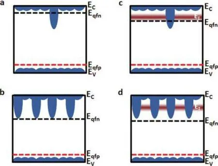
Fig.1.Schematic of the energy bands in quantum dot films (a) comprised of predominantly a single size of QDs with a small addition of a smaller bandgap QD; (b) possessing many inclusions of small bandgap QDs; (c) dominated by a trap density near the CB; and (d) affected by both traps and substantial small bandgap inclusions. Eqfn and Eqfp signify the electron and hole quasi-Fermi levels,respectively. Ec and Ev are the quantum-confined conduction and VB energies.[18]
In addition,not all exciton recombination emits photons,and some of them will dissipate energy in the form of heat or vibration,as shown in Fig.2.Exciton recombination has a variety of attenuation channels competing with each other.Possible attenuation channels include radiative recombination of emitted photons,non-radiative recombination assisted by trap states in the energy gap, energy transfer to adjacent QDs or charge transport layers, charge transfer through the interface or Auger recombination, and field-induced exciton dissociation processes.[23]
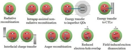
Fig.2.Schematic diagram of possible exciton attenuation process in QLED.[24]
2.2.QLED luminescence mechanism
The working principle of QLED can be explained by direct charge injection or Forster energy transfer(FRET)mechanism,or both,as shown in Fig.3.[25]
QLED is a light-emitting device stacked with multi-layer films.The structure and working principle of the device are shown in Fig.3(a).As a typical injected electroluminescent device,QLED luminescence can be divided into the following six processes:(i)Holes and electrons are injected into the hole and electron transport layers from positive and negative electrodes, respectively.(ii) Holes and electrons are transmitted in hole and electron transport layers, respectively.(iii) Holes and electrons are injected into the QD layer under the action of external electric field.(iv)Electrons and holes form excitons in QDs.(v) Excitons radiate and recombine to emit photons.(vi) Photons pass through each functional layer and are injected into the device.[26]Therefore,we can only optimize the performance of the device by reducing the carrier transport energy level barrier,[27,28]improving the carrier mobility of the material,[29,30]balancing the carrier injection,[31]improving the exciton formation and radiation recombination probability in QDs,and improving the photon emission efficiency.
FRET,also known as resonance energy transfer,is also a commonly discussed luminescence mechanism.As shown in Fig.3(b).Electrons and holes converge in the carrier transport layer and form excitons.The exciton energy of the transport layer is greater than that of the quantum dot, which is transferred to the quantum dot in the form of a non-radiative transition and excites the quantum dot to emit light.[32,33]QLED emission is dominated by direct injection, and FRET consumes additional charge carriers.
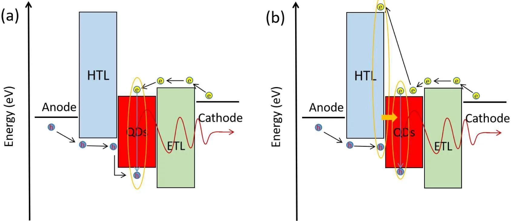
Fig.3.(a)Schematic diagram of charge injection mechanism and(b)schematic diagram of FRET capability transfer.
2.3.Influence factors of QLED luminous efficiency
The luminescence efficiency of a device is generally described by the external quantum efficiency (EQE), which is defined as the ratio of the number of photons emitted from the device to the number of electrons injected into the device.The expression of EQE of QLED device is
whereγrepresents the proportion of excitons formed by the injected carriers;ηrcrepresents the radiative recombination probability of excitons; andηoutrepresents the ratio of the number of photons emitted from the device to the number of photons produced.In addition,the product ofγ,ηrcis defined as the in-device quantum efficiency(IQE).[34]
This paper analyzes these four factors respectively.
(i)γis the exciton formation rate of the device, which can also be understood as the ratio of the exciton composite current to the total current of the device.The exciton formation rate can be increased by suppressing the invalid current of the device.The device current mainly includes the compound current of QD layer,the bypass current formed by carrier overinjection, and the invalid current caused by the trap between QD and carrier transport layer.[35]In order to suppress the bypass current of the device,it is necessary to improve the energy level matching and mobility,and balance the charge carrier injection.In order to suppress the ineffective current,it is necessary to purify the material,improve the film morphology,and reduce the trap density.
(ii)ηrcis the radiative recombination probability of exciton.Non-radiative recombination caused by surface traps of QD, the energy transfer and charge transfer between QDs and the transport layer, and the Auger recombination caused by a large number of charged QDs can all cause the decrease ofηrc.Through core-shell structure, alloying and surface ligand treatment, the surface traps of QDs can be reduced,and the non-radiative recombination and Auger recombination caused by traps can be improved.The charge transfer and nonradiative recombination between QDs and transport layers can be inhibited by optimizing the transport layer materials or the interface between QDs and transport layers, thus improving the probability of radiative recombination.In 2022, Xuyong Yanget al.developed a dielectric-QD-dielectric sandwich structure,which can modulate the energy band alignment,thus shifting the exciton recombination zone in the QD layer.[36]
(iii)ηoutrepresents the ratio of the number of photons emitted from the device to the number of photons produced.Before the photon is emitted from the device,it passes through the absorption and refraction of multilayer films and the reflection of multiple interfaces, so the output light index is determined by the film thickness, refractive index, extinction coefficient,etc.of each layer of the device.In order to increase the light yield of the device,the throughput of the transmission layer and transparent electrode should be increased as much as possible.At the same time,the thickness of the reflective side transmission layer can be adjusted to make the luminescent layer of the device meet the condition of interference phase length.[37,38]
3.QDs material
Due to the small size and large specific surface area of QDs, the exposed surface of QDs is prone to producing excessive traps,and some excited electrons will relax to the surface trap level,leading to the increase of exciton non-radiative energy transfer and the reduction of photoluminescence efficiency.Many studies have shown that core-shell QDs with thick shells,gradient alloyed QDs and QDs modified with organic ligands can improve the luminescence performance of QDs.[39]
3.1.Core-shell QDs
It is well known that the exposed CdSe is very sensitive,and the surface is easy to be oxidized, resulting in a series of traps,which will reduce the performance of QDs and limit the application of QDs.[40,41]Growing shells on the surface of QDs can well passivate surface traps,effectively reduce traps caused by water and oxygen erosion,and improve the stability and quantum yield of QDs.Therefore,the core-shell structure of QDs has developed rapidly.[42]
In core-shell QDs,a semiconductor core and a semiconductor shell are included so the potential energy distribution of carriers is formed.[43]The optical and electronic properties of a core-shell quantum dot are determined by the band gap between its core and shell.Core-shell QDs can be divided into three categories according to the relative positions of the band gaps between the core and shell materials, as shown in Fig.4.[44]
(a)Type I QDs In type I QDs,the band gap of the shell is larger than that of the core,that is,the VB and CB of the core of the quantum dot are located between the band gaps of the shell material, and the shell material can completely restrict electrons and holes in the core.CdSe/ZnS QDs are typical type I QDs.[45,46]In this structure,the growth of the shell can well passivate the QD core,reduce the surface trap states,enhance the resistance to photodegradation and thermal stability,and improve the fluorescence quantum yield.
(b)Reverse-type-I QDs In reverse-type-I QDs,the band gap of the shell material is smaller than that of the core,and by adjusting the thickness of the shell, electrons and holes can be partially or completely delocalized in the shell region,[47,48]thus causing obvious red shift of the absorption spectrum.[49,50]
(c)Type II QDs In type II QDs,the VB edge or CB edge of the shell is located in the band gap of the nuclear QDs,and the energy level of the shell material and the nuclear level of the QDs are misarranged so that the holes and electrons are spatially separated in different regions of the core/shell QDs.[51-53]The effective band gap of type II core/shell QDs depends on the band shift of the core and shell materials,and the band gap between the core and shell materials can be adjusted by changing the thickness of shell and core size.
(d) Quasi-type-II QDs In quasi-type-II QDs, the band gap of the shell material is slightly wider than that of the core,and the band offset of the CB or VB is small, for example,CdSe/CdS QDs, in which the holes are confined in the CdSe core,but the electronic wave function can be delocalized to the shell.[54-56]
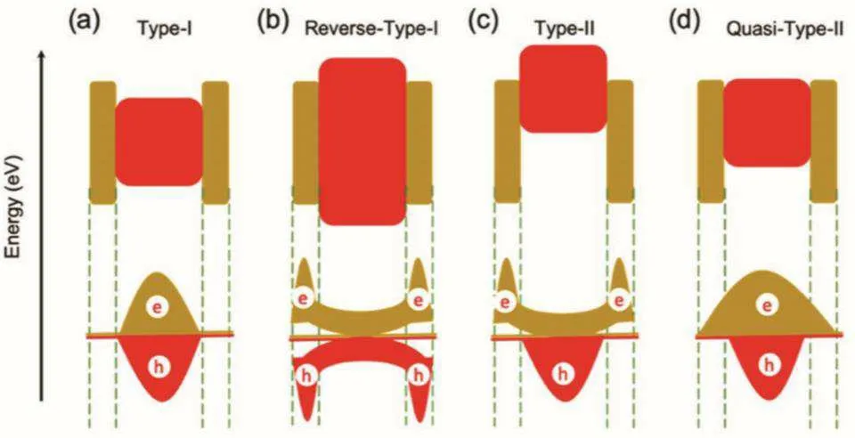
Fig.4.Schematic diagram of three kinds of QDs.[44]
3.2.Gradient alloying of QDs
The core and shell structure of QDs has different lattice parameters - there is a lattice mismatch problem.It is easy to produce traps between the core and the shell, which become the recombination center and provide a channel for nonradiative Auger recombination,leading to the reduction of fluorescence yield of QDs.[57-59]
Based on the Auger ionization model, Cragg and Efros theoretically proved that Auger recombination is caused by heterogeneous interfaces or interface traps.They introduced gradient alloy shells into core-shell QDs, effectively suppressing the probability of non-radiative Auger recombination(Fig.5).[60]Compared with traditional core-shell QDs,the introduction of alloy layers can effectively alleviate the lattice mismatch at different shell interfaces, flatten energy levels,and reduce interface traps.[61]
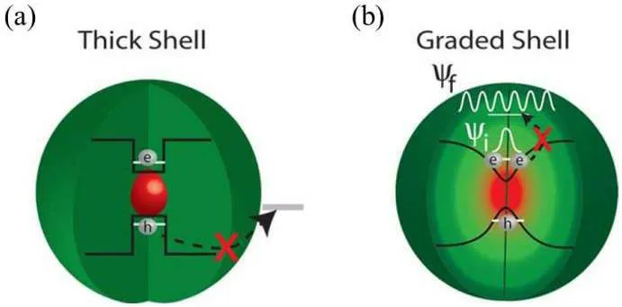
Fig.5.(a)Defect-trapped carriers in core-shell QDs.(b)Gradient alloy layer inhibits Auger recombination.[62]
In addition, although the fluorescence spectra of CdSe QDs with different particle sizes can cover the full range of the visible spectrum, the fluorescence spectra of QDs with green and blue luminescent core-shell structures are difficult to synthesize because the electron wave function is delocalized into the shell, which weakens the domain limiting effect of QDs accordingly.By introducing a wide band gap material to form an alloy, the band gap of QDs will be widened, and the fluorescence spectrum will be blue shifted.Therefore,introducing wideband gap materials to CdSe QDs to form alloy structure is a feasible way to achieve blue and green luminous QDs.In 2003,Professor Zhong Xinhua synthesized ZnCdSe QDs with ternary alloy structure by using a CdSe core to coat ZnSe, a wide-band gap material, and then realizing ionic diffusion at high temperatures.[63]By adjusting the precursor material of the reaction, the spectral range was continuously adjustable from 500 nm to 580 nm, and the fluorescence quantum yield was higher than that of non-alloy QDs.
Subsequently, different components of alloy QDs have been studied in depth.[46,64,65]In 2015,Qian Leiet al.synthesized CdSe/Cd1-XZNxSe1-YSY/ZnS core/shell QDs (Fig.6).The Cd1-XZNxSe1-YSYinterface layer was sandwiched between the CdSe-rich core and the ZnS-rich shell layer, and the middle Cd1-XZNxSe1-YSYinterface layer was alloyed in a hierarchical way.The gradual change in composition from the CdSe-rich core to the ZnS-rich outer shell layer is able to alleviate lattice stress caused by lattice mismatch and thus improve PLQY.[66]At the same time,some research groups used CdSeS ternary alloy structure to synthesize CdS,which has a larger band gap and stability than CdSe materials.[67]
In summary,on the one hand,the lattice mismatch can be reduced by the alloy method to improve the fluorescence quantum yield.On the other hand,the quantum confinement effect of QDs on electron and hole wave functions is adjusted by different alloy method.For QDs with different luminescence spectra that can be synthesized by adjusting their structure,the interface alloy method or gradual alloy method is often used to achieve fluorescence QDs full visible spectral range.[68,69]
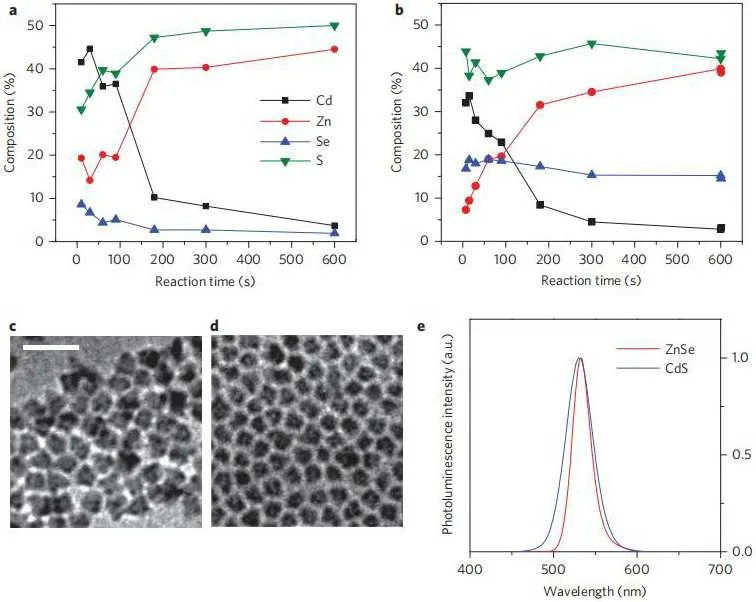
Fig.6.Surface elemental composition evolution with reaction time by XPS characterization, TEM characterization and photoluminescence spectra of green QDs.(a)Composition evolution of CdS-rich QDs.(b)Composition evolution of ZnSe-rich QDs.(c)TEM image of CdS-rich QDs(scale bar,25 nm).(d)TEM image of ZnSe-rich QDs(scale bar as in(c)).(e)Photoluminescence spectra of CdS-rich(blue)and ZnSe-rich(red)QDs.[66]
3.3.Organic ligand modified QDs
Ligands can affect the properties of QDs in many aspects:the functional groups of ligands can affect the solubility of QDs, making the QDs more stable; the ligand can be combined with the suspended bond on the surface to passivate the surface activity and effectively reduce the trap state on the surface.The electrical characteristics of the surface ligand and the length of the carbon chain will affect the carrier transport rate in the QDs film.According to the characteristics of the ligand,the classification design of the surface of QDs can predict and optimize the electronic characteristics of colloidal QDs,and it is also the key to optimizing the LED of QDs.
In order to blunt the surface traps of QDs,long chain organic ligands such as phosphoric acid,long hydrocarbon chain fatty acids or amine functional groups are grown on the surface of QDs during the synthesis process.[70-72]However,the presence of long-chain ligands is a double-edged sword.[73]On the one hand,the long-chain ligands on the surface of QDs can improve the dispersion of QDs and avoid agglomeration.On the other hand,these long-chain ligands exhibit insulating properties,which inhibit the transport of carriers in the luminescent layer,increase the difficulty of carrier injection into QDs,and increase the probability of Auger recombination, and accelerate the efficiency roll-off of devices.Therefore, to ensure the optical properties and stability of QDs,short-chain ligands instead of long-chain ligands are used to improve the charge carrier injection efficiency in QLED, thereby improving the luminescence efficiency while reducing the efficiency roll-off.
In 2015, Shenet al.used 1-octanthiol (OT) as the ligand to replace the oleic acid (OA) ligand on the surface of blue ZnCdS/ZnS core-shell QDs.As shown in Fig.7, after ligand exchange, the electron mobility of the QD luminescent layer was increased by 2 times, and the hole injection was promoted, resulting in a maximum EQE of 12.2%and a maximum luminance of 7600 cd/m2for the blue-purple QLED.[74]Subsequently, Shen’s group used 1,1,1-Tris (Mercaptomethyl)nonane (TMMN) ligands to replace the original OA ligands on the QDs surface.The surface of QDs after the ligand exchange was more passive and the insulation layer was thinner.The highest EQE of QLED after the TMMN treatment reached 16.5%, increasing by 50%.The excellent performance of the device was attributed to the improved charge injection/transport and charge injection balance of the shortchain TMMN ligand.[75]

Fig.7.(a)1 H NMR spectra of as-synthesized QDs with OA as ligands(upper panel)and QDs after ligand exchange with OT(lower panel).Inset:molecular structure of OA and OT.(b)Dynamic light scattering(DLS)spectra of QDs with OA and OT as ligands.(c)Current-density-voltage(J-V)characteristics of electron-and hole-only devices based on 40 nm thick QDs with OA and OT as ligands.[74]
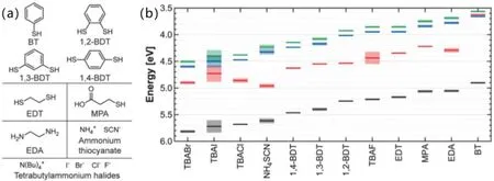
Fig.8.Ligand-dependent energy levels measured by UPS.(a)Chemical structures of the ligands employed in this study.(b)Complete energy level diagrams of PbS QDs exchanged with the ligands shown in panel(a).[78]
Previous studies have reported that ligands of 6-8 carbon chains are usually used to exchange the QDs surface by solution method,but the process of ligand exchange often leads to the decrease of photoluminescence quantum yield(PLQY)of QDs.[74,76]If the chain length of ligand is shorter,the solubility of QDs would be reduced and the film formation would be poor after the solution method exchange,which is not conducive to the improvement of QLED performance.Solid state ligand exchange can avoid this disadvantage.In 2018, Sargentet al.used the solid-state ligand exchange method to replace the organic ligands on the QD surface with a chlorinated reagent (SOCl2) as an inorganic monatomic layer surface ligand.[77]SOCl2can react with the carboxyl group in OA, thus removing the OA ligand and binding the conductive chloride ligand to the QD surface.More importantly,the PLQY of QD films remained unchanged(60±2%)after chlorination, and there was no obvious red shift in fluorescence peak positions.Surface chlorination promotes charge injection,moderates electron and hole aggregation near the electron transport layer(ETL)and hole transport layer,and suppresses non-radiative Auger recombination at high injection current densities.The chlorinated QLED’s on-off voltage is reduced from 3.5 V to 2.5 V, resulting in a maximum luminance of 460000 Cd/m2.Therefore,substituting the long-chain ligand with the short-chain ligand based on the solid-state ligand exchange method is of very important guiding significance in inhibiting the roll-off of the efficiency reduction of non-radiative Auger recombination.
The surface ligands of QDs not only affect the mobility of charge carriers,but also cause changes in their energy level positions.In 2014,Brownet al.studied the energy level structure of PbS QDs with different ligands.The results of ultraviolet photoelectron spectroscopy(UPS)showed that the energy level positions of QDs modified by different ligands were different.Due to the interface polarization between the quantum dot and the surface ligand,the ligand containing the electrondonating group can move the quantum dot energy level up,while the ligand containing the electron-withdrawing group can cause the quantum dot energy level to move down, as shown in Fig.8.[78]In the same year, Liuet al.used electrochemical methods to deeply study the effects of different surface ligands on the energy level structures of CdSe,CdTe and alloy CdSexTe1-XQDs, and their experimental results were similar to those reported previously.[79]
4.Device engineering
In 1994,Alivisatoset al.reported the first QLED device,in which the QD luminescence layer and PPV hole transport layer were embedded between two electrodes,and the charge carriers were injected into the QD layer through the cathode with low power function or the anode with high power function to generate composite luminescence.[13]However, this most primitive structure was accompanied by a large amount of exciton quenching, and the luminous efficiency was only 0.01%.In order to prevent quenching phenomenon,balanced carrier injection and improved radiation recombination, hole injection layer,hole transport layer and electron transport layer were added on the basis of the original structure,as shown in Fig.9, and finally the commonly used QLEDs structure was obtained.[80,81]The subsequent development of QLEDs devices is based on the structure of Fig.9(c).Because QLED is a multi-layer thin film structure, the energy level structure,carrier mobility and optical properties of these materials are different,and the layer thin film structure will introduce multiple interfaces,which will also affect the device’s performance.
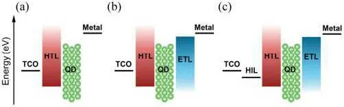
Fig.9.Structure of different QLED devices.[81]
4.1.Hole injection layer
In common OLED and QLED structures, ITO usually acts as a transparent anode with a work function of about-4.7 eV.Due to the large difference between its work function and the energy level of the hole transport layer material,in order to form ohmic contact, a buffer layer is usually inserted between the two, so that holes can be better injected into the hole transport layer to improve the performance and efficiency of the device.[82]
In order to improve the efficiency of hole injection, hole transport materials with high mobility and relatively deep highest occupied molecular orbital (HOMO) energy level should be selected.On the other hand,for a given hole transport layer,it is necessary to optimize the electrode to improve the electrode function and increase the hole injection from the electrode to the hole transport layer.As shown in Fig.10(a),when the work function of the hole injection layer is deeper than theEICT+energy level of the organic hole transport material,the electrons of theEICT+of the transport material will spontaneously transfer to the injected material with lower energy, and the band bending occurs at the HIL/HTL interface until the electrons are fully transferred.The work function of the injection end is flush with theEICT+energy level of the transport layer.[83,84]Meanwhile, the hole transport layer material loses interface electrons to formσ+, which is conducive to hole injection in the device.Peter Hoet al.carefully studied the hole-injection interface between PEDT and the polymer OC1C10-PPV hole-transport layer,and observedσ+state aggregation at the interface by electro-absorption (EA)experiments.[85,86]They found that deepening the substrate work function increased the work-function difference between theEICT+levels of the substrate and the polymer,resulting in more intense electron exchange between the polymer and the substrate, and a further increase in hole injection into the device(Fig.10(b)).PEDOT:PSS is the most widely used hole injection(HIL)material,and increases the work function of ITO electrode from-4.7 eV to-5.1 eV,forming Fermi level pinning with TFB.However, after modification of PEDOT:PSS by solution or small molecules, the work function of the injection layer will continue to increase, and the hole injection efficiency of the device will continue to improve.[87]
At present, the commonly used hole injection material is PEDOT:PSS, but its acidity and water absorption will corrode the ITO electrode and affect the stability of the device.[88,89]Therefore, a material with similar energy levels to PEDOT:PSS, but with good environmental stability, is needed to replace PEDOT:PSS.Transition metal oxides come into view in this situation.
Compared with PEDOT:PSS, transition metal oxides have the following advantages: high hole mobility,high transparency, appropriate work function, and good environmental stability.[82]Metal oxides can be used as ideal material for hole injection layer.Among them,relatively widely studied oxides include nickel oxide (NiOx), tungsten oxide (WO3), molybdenum oxide (MoO3), vanadium pentaoxide (V2O5), copper oxide(CuO),cuprous oxide(Cu2O)and so on.
Compared with other oxides,nickel oxide,as a typical Ptype transparent semiconductor material, not only has good hole transport ability, but also has electronic blocking ability, which has been widely studied in batteries, OLED and QLED.[88,90]I-min Chanet al.deposited an ultra-thin NiO layer on ITO by magnetron sputtering.The addition of NiO thin layer reduced the hole injection barrier and enhanced the hole injection ability.[91]Since then, the research of nickel oxide in optoelectronic devices has become more and more extensive.In 2014, Xiaoyong Lianget al.used nickel oxide nanoparticles in devices,and their performance was improved to a certain extent.[92]
Molybdenum oxide and tungsten oxide are also of great concern.In 2013, Xuyong Yanget al.used WO3nanoparticles to replace PEDOT:PSS as the hole injection layer, and the EQE of the device reached 3.32%,the brightness reached 30006 cd/m2, and the lifetime was also greatly improved.[93]They further passivated WO3with chlorine to further extend the device lifetime (T50>105h under an initial luminance of 100 cd/m2).[94]Notably, the team reported an MoO3as HIL inverted green QLED capable of achieving a 96.42 cd/A current efficiency and a 25.04% EQE.[95]Seong Jun Kanget al.reported that the maximum luminance and current efficiency of the QLED with V2O5:Li (10%) HIL were measured as 152140 cd/cm2and 22.07 cd/A.[96]Xiaowei Sunet al.replaced PEDOT:PSS with WO3as HIL, and the lifetime of QLED was doubled.[97]Yidong Zhanget al.also reported the QLED with WO3as the HIL, and the QLED’s lifetime reached 11844 h, 40% longer than the lifetime of the device with PEDOT:PSS.[98]
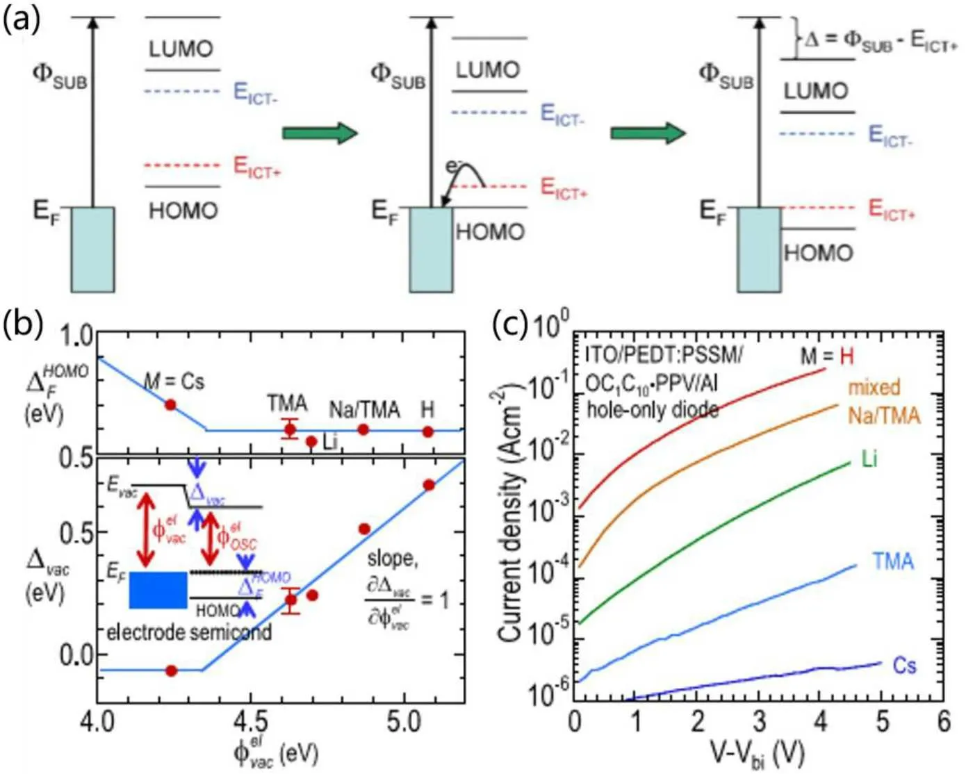
Fig.10.(a)Schematic diagram of pinning effect at Fermi level.[84](b)Fermi level pinning phenomenon of different functional substrates and(c)corresponding J-V characteristic curves of single hole devices.[87]
4.2.Hole transport layer
QLED has been in development for nearly 30 years.The process of hole injection still needs to overcome a large barrier, and mobility is very low.The hole injection ability is always weaker than the electron.Therefore, the hole transport layer first needs to have good hole injection ability.In addition,other properties of the hole transport layer material,such as electronic barrier ability, film formation uniformity,trap state and stability,should be considered.
In 2002, Bulovicet al.took OLED device structure as reference and realized a pure quantum dot LED device for the first time with monomer TPD as hole transport layer.[99]The energy level structure of TPD is suitable for hole injection, but the film forming quality of small molecules is very poor and the surface is rough, so problems have arisen in the preparation process.At the same time,monomer TPD is very unstable and easy to recrystallize during work.In 2006,Gingeret al.formed PS-TPD-PFCB and BiVB-MetPD polymeric materials through cross-linking,which significantly improved the stability of hole transport materials.[100,101]In 2007,Academician Li Yongfang’s group used poly-TPD polymer hole transport layer to further improve the device performance.[102]Poly-TPD is a high polymer of TPD.The physical and chemical properties of poly-TPD materials are more stable thus the hole transport performance is significantly improved.The film formation is more uniform,and octane and other solvents are not able to wash it away.Since then, other organic polymers with trianiline hole groups have also been widely used in QLED device hole transport layer, these materials have a suitable HOMO energy level and good hole mobility,and can block electrons.[103]
Polymers such as poly-TPD,TFB(hole transport material poly[9, 9-dioctyfluoren-co-N-(4-butylphenyl)dianiline])and PVK (poly [9-ethylene carbazole]) are the most commonly used QLED hole transport materials.The molecular structure,HOMO and LUMO energy levels and hole mobility of the material are shown in Table 1.[29,104]Similar to poly-TPD, TFB conducts holes through the trianiline group, and the HOMO level is about-5.2 eV∼-5.3 eV.The HOMO of PVK is even deeper,at-5.8 eV,but the mobility is two orders of magnitude smaller than that of the first two materials.The hole injection capability of the device is directly related to the level barrier of the anode interface and the mobility of the hole transport layer.The hole transport layer materials should be selected according to the specific quantum dot energy level structure.When the VB of QDs is shallow, both TFB and poly-TPD are good hole transport materials.However,some QDs have very deep VB.In this case,PVK materials with a deeper HOMO should be used to inject holes into the QDs in order to improve the efficiency of the device.Unfortunately,due to the low mobility of PVK and the difficulty of hole injection from electrode to PVK,PVK is not suitable to be used as a hole transport layer alone.In 2014, Daiet al.used a poly-TPD (chlorobenzenesolvent)/thin PVK(m-xylene solvent)composite stacked hole transport layer to partially solve the hole injection problem of PVK materials,enabling devices to have better electrical properties,lower turn-on voltage,and maintain high luminescence efficiency.Compared with the single-layer PVK hole transport layer,the composite stacked hole transport layer conducts holes through poly-TPD,and the hole injection transport ability is improved.At the same time,the holes of the device enter the QDs through the PVK interface layer, thus improving the luminescence performance of the device.

Table 1.Performance summary of common organic polymer hole transport layers.[29,104]
In addition, incorporation of small organic molecules or metal salts into the polymer can significantly improve the carrier mobility of the polymer, which is conducive to the hole injection of the device.Researchers such as Chae and Liao doped TCTA organic small molecules and Li salt(Li-TFSI)in PVK, respectively, to improve the current density and luminescence efficiency of the device.[105]And F4-TCNQ,molybdenum oxide, HAT-CN and other deep LUMO level N-type semiconductors are also typical polymer doping materials.Electrons from the polymer can be transferred to the doped material,thereby increasing the hole concentration in the hole transport layer and hence the hole mobility.[106,107]
Some researchers further improve the performance of the hole transport layer by cross-linking or modifying the molecular structure.Recently,Tanget al.cross-linked TFB and HTM CBP-V small molecules,which deepened the HOMO level of TFB material and significantly improved the efficiency and lifetime of the device(Fig.11).[108]By optimizing the molecular structure, Baiet al.introduced sp2hybrid N atoms into PVK to form PVI.PVI increased the HOMO level of PVK from-5.8 eV to-6.0 eV, which also slightly improved the device efficiency.[109]Xuyong Yanget al.inserted two layers of MoO3into the CBP to improve lateral current spreading,which made the device exhibit the maximum current efficiency of 88.7 cd/A and the maximum EQE of 20.6%.[110]
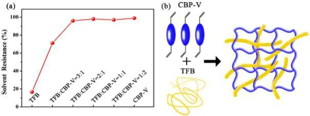
Fig.11.(a) Solvent tolerance of TFB:CVP-V after cross-linking.(b)Schematic diagram of the cross-linking process.[108]
In addition to polymer materials,small molecule materials such as TCTA and CBP are often used in the hole transport layer of the inverted devices.Star materials such as DNA-CTMA(-0.9 eV∼-5.6 eV),graphene oxide(GO)and CuSCN(-1.8 eV∼-5.5 eV)with appropriate energy levels have also been applied to QLED devices.[111,112]Suitable new hole transport layers are likely to lead to new breakthroughs in devices.
4.3.Electron injection layer
In order to block holes and limit the compound zone,the electronic transfer material shall have higher electron mobility, appropriate CBM or LUMO level.Valence band maximum (VBM) or HOMO energy levels are required for electrons to be injected into the QD layer without overcoming a large potential barrier.Organic materials such as Alq3(octahydroxyquinoline aluminum) and TPBi (1,3,5-tri (1-phenyl-1H-benzimidazole-2-yl)benzene)are usually used in the early electron transport layer.The LUMO level is lower than 3.0 eV,and it is difficult for electrons to be injected into these organic transport layers from electrodes, resulting in low electron injection efficiency of devices.[99,113]Operating voltage is very high.The electron mobility of organic small molecule electron transport materials is usually 1-3 orders of magnitude lower than that of organic hole transport materials.At the same time,the LUMO level of organic small molecule electron transport materials is high,usually higher than-3 eV,while the CBM of QDs is usually lower than-3.5 eV,and the CBM of red QDs is about-4 eV∼-4.4 eV.If organic small molecule ETL is used,electron injection into QDs from organic ETL will have to overcome a large energy level difference,which is not conducive to electron injection.In addition,the HOMO of organic ETL material is relatively shallow,and its hole-blocking ability is weak, so it cannot restrict the composite region well.QLED devices employing organic small molecule ETL have rarely been reported because of these disadvantages.
In 2008, Bawendi group applied ZnO to QLED devices for the first time, using ZnO:SnO2as the electron transport layer, which effectively reduced the device opening voltage.[114]However,a combination of solution and vacuum deposition processes complicates the QD-LED fabrication process and reduces the throughput compared to all solution-based manufacturing techniques.In 2011, Lei Qianet al.created S-QLED device by using ZnO nanocrystal electron transport layer.[115]With ZnO nanocrystals as the electron transport layer and organic polymers as the hole transport layer, most of the carriers in the device can be transported to the quantum dot layer and emit light in the quantum dot layer.The S-QLED is the structure choice of most high-performance devices at present.
There is a strong interfacial interaction between QDs and ZnO nanocrystals electron transport layers.Non-radiative recombination, energy transfer and charge transfer of the interface will reduce the luminescence efficiency of QDs.In 2014,Penget al.inserted a thin layer of PMMA between red QDs and ZnO nanocrystals,and the device current decreased significantly under the same voltage.However,the luminance of the device basically remained unchanged,so the luminescence efficiency increased significantly.[31]The fluorescence lifetime of QDs immediately decreases from 21.6 ns to 10.6 ns when a thin layer of ZnO nanocrystals is spun on the QD film.However,when a thin layer of PMMA material of 6 nm is inserted between the QDs and ZnO nanocrystals,the fluorescence lifetime of QDs is restored to 19.5 ns,which indicates that the fluorescence quenching effect of ZnO nanocrystals on QDs can be effectively suppressed by adding a thin layer of PMMA.However, PMMA is an insulating material so the electronic injection of the device will be seriously hindered, leading to the increase of the device opening voltage and the decrease of the luminescence efficiency.As an alternative to PMMA,Al2O3,PEIE and other insulating film layers can also improve the interface, but the insulating materials will greatly inhibit the injection of electrons, and the film thickness needs to be strictly controlled during preparation which is very difficult to process.[116,117]
Researchers then found that the interfacial interactions could be inhibited by optimizing the composition and structure of ZnO nanocrystals.In 2017,Chen’s group added a thin layer of Zn0.85Mg0.15O nanocrystals between ZnO nanocrystals and QDs.Through fluorescence lifetime test and fluorescence quantum yield test, it was confirmed that thin layer Zn0.85Mg0.15O nanocrystals could improve the interface interaction between QDs and electron transport layers.At the same time, they observed that the visible light fluorescence of Zn0.85Mg0.15O nanocrystals was weaker, suggesting that the oxygen vacancy traps on the surface of nanocrystals were improved, and the non-radiation channels and hole transfer channels of QDs were effectively suppressed.[118]However,in 2016,Lei’s group found that small-sized ZnO nanocrystals could better inhibit QD quenching,with larger specific surface area,more surface traps and stronger visible light fluorescence intensity.[119]The experimental phenomena and conclusions of Chen’s group and Lei’s group were exactly opposite.Even now,the correlation between the visible light fluorescence intensity of ZnO nanocrystals,the surface trap state,and the ZnO nanocrystals/QDs interface interaction is not clear.In addition, doping of various ZnO nanocrystals and surface ligand exchange treatment can also reduce interface interactions,but the intrinsic relationship between specific material regulation and device performance remains to be studied.[120,121]
5.Conclusion and perspectives
Over the past 30 years,researches on QLEDs have come a long way in improving performance and understanding underlying mechanisms.This paper reviews the development of QLED materials and device structures,and tries to summarize some factors that affect the performance of QLED devices.In the following,several key strategies for improving device performance are summarized.
(i)High-performance quantum dot materialsMany attenuation channels compete for exciton recombination in QDs,including radiative recombination of emitted photons, nonradiative recombination assisted by trap states in the energy gap, energy transfer, Auger recombination and field-induced exciton dissociation.It is necessary to design the core-shell and gradient alloy structure of QDs to passivate surface traps and improve the PLQY of QDs.In addition, surface ligand engineering is also needed to improve the luminescence efficiency of QDs,optimize the electrical properties of QDs,and improve the charge injection and transport capabilities in order to further improve the performance of QLED.
(ii)Device engineeringQLED luminescence includes the processes of carrier injection,transmission,excitons forming,recombination luminescence and light emission.It is necessary to design appropriate structures and select appropriate materials to reduce the carrier transmission level barrier, improve the carrier mobility of materials, balance carrier injection, improve exciton formation and radiation recombination probability in QD,and improve photon emission efficiency,so that devices can have good performance.
In addition to interfacial interactions, the electron injection capability of ZnO nanocrystals is also important.The electron injection ability of ZnO nanocrystals is too low, and the device needs very high operating voltage.However,if the injection capacity of ZnO nanocrystals is too high,the carrier injection balance of the device will be affected, and the over injected electrons will accumulate in the quantum dot layer,which will affect the device’s performance.On the one hand,a large number of electrons are accumulated in the quantum dot layer,and the electron transfer between the quantum dot layer and the hole transport layer increases the invalid current ratio of the device,and the quantum dot with multiple electrons will also produce Auger recombination,which will eventually lead to the decrease of the luminescence efficiency of the device.On the other hand, QDs in the charged state for a long time are also prone toin situelectrochemical reduction,resulting in impaired luminescence performance of QDs and affecting the stability of devices.
(iii) High performance hole transport materialsZnO nanoparticles enhance the electron injection ability of QLED,while the main hole transport materials are still limited to a few organic materials.Low hole mobility leads to the imbalance of carrier injection,which is not conducive to the improvement of the luminous efficiency and stability of devices.Especially in blue QLED,the huge energy level barrier seriously affects the hole injection efficiency.The development of hole transport materials with deep HOMO energy levels and high hole mobility is of great significance for achieving high efficiency blue QLED.
Acknowledgments
Project supported by Leading innovation and entrepreneurship team of Zhejiang Province of China (Grant No.2021R01003), Science and Technology Innovation 2025 Major Project of Ningbo(Grant No.2022Z085),Ningbo 3315 Programme (Grant No.2020A-01-B), YONGJIANG Talent Introduction Programme(Grant No.2021A-038-B),and Zhujiang Talent Programme(Grant No.2016LJ06C621).
- Chinese Physics B的其它文章
- Diamond growth in a high temperature and high pressure Fe-Ni-C-Si system: Effect of synthesis pressure
- Multi-channel generation of vortex beams with controllable polarization states and orbital angular momentum
- Calibration of quantitative rescattering model for simulating vortex high-order harmonic generation driven by Laguerre-Gaussian beam with nonzero orbital angular momentum
- From breather solutions to lump solutions:A construction method for the Zakharov equation
- Complete population transfer between next-adjacent energy levels of a transmon qudit
- Ultralow-temperature heat transport study of noncentrosymmetric superconductor CaPtAs