
Radiation tolerance studies on the VA32 ASIC for DAMPE BGO calorimeter∗
2014-04-24 09:28GAOShanShan高山山FENGChangQing封常青JIANGDi蒋荻LIUShuBin刘树彬ZHANGZhanGang张战刚XIKai习凯andANQi安琪
Nuclear Science and Techniques 2014年1期
GAO Shan-Shan(高山山),FENG Chang-Qing(封常青),,JIANG Di(蒋荻),LIU Shu-Bin(刘树彬),ZHANG Zhan-Gang(张战刚),XI Kai(习凯),and AN Qi(安琪)
1State Key Laboratory of Particle Detection and Electronics(IHEP-USTC),Hefei 230026,China
2Department of Modern Physics,University of Science and Technology of China,Hefei 230026,China
3Institute of Modern Physics,Chinese Academy of Sciences,Lanzhou 730000,China
Radiation tolerance studies on the VA32 ASIC for DAMPE BGO calorimeter∗
GAO Shan-Shan(高山山),1,2FENG Chang-Qing(封常青),1,2,†JIANG Di(蒋荻),1,2LIU Shu-Bin(刘树彬),1,2ZHANG Zhan-Gang(张战刚),3XI Kai(习凯),3and AN Qi(安琪)3
1State Key Laboratory of Particle Detection and Electronics(IHEP-USTC),Hefei 230026,China
2Department of Modern Physics,University of Science and Technology of China,Hefei 230026,China
3Institute of Modern Physics,Chinese Academy of Sciences,Lanzhou 730000,China
The Dark Matter Particle Explorer(DAMPE)is being constructed as a scientific satellite to observe high energy cosmic rays in space.As a crucial detector of DAMPE,the BGO calorimeter consists of 1848 PMT dynode signalswhichbringdiff i cultiesinfront-endelectronicsonthespace-limitedandpower-limitedsatelliteplatform. To overcome the challenge,a low-noise,low-power and high-integration ASIC chip,named VA32HDR14.2,is taken into account.In order to evaluate the radiation tolerance of the chip in space radiation environment,both single event effect(SEE)and total ionizing dose(TID)tests were performed.The SEE test result shows that the effective linear energy transfer(LET)threshold of single event latch-up(SEL)of the chip is around 23.0MeV-cm2/mg,which is relatively sensitive,thus protection methods must be taken in the electronics design.The TID test result shows that the TID performance of the chip is higher than 25Krad(Si),which satisf i es the design specif i cation.
Radiation effects,SEE,TID,ASIC,VA32HDR14.2
I.INTRODUCTION
The radiation effects of semiconductor devices,induced by particles and rays in harsh space radiation environment,could cause damage to the satellites[1].Many types of radiation effects have been found and studied.Among those,SEE and TID,which are contributed by protons and electrons in the Van Allen belts,and protons and heavy ions from cosmic rays and solar f l ares,are typically the focus of attention[2,3].
DAMPE is a scientif i c satellite aimed for cosmic ray study, gamma ray astronomy,and searching for the clue of dark matter particles by investigating the composition and energy spectra of primary cosmic rays[4,5].It is designed to f l y on a near-earth orbit with an altitude of 500km and an inclination of 97 degrees for a mission period of at least 3 years. One crucial payload of the satellite is the BGO calorimeter, which is composed of 308 BGO crystals and 616 Photomultiplier Tubes(PMTs).There are 1848 PMT dynode signals need to be measured,which bring diff i culties in the design of front-end electronics[6].To overcome this challenge,a 32-channel charge measurement application specif i c integrated circuit(ASIC),named VA32HDR14.2(VA32),is taken into account and used for DAMPE prototype[7,8].According to the design specif i cation,the SEL threshold of the electronics for the calorimeter should be higher than 37.0MeV-cm2/mg while the TID performance should be higher than 20Krad(Si), otherwise protection methods should be applied.To evaluate the radiation tolerance of VA32,SEE and TID tests should be carried out.
II.DEVICE CHARACTERISTICS
The VA32HDR14.2 is designed by a company named IDEAS in Norway and manufactured with the 0.35µm CMOS technology processed on epitaxial silicon wafer[9].As shown in Fig.1,each VA32 chip has 32 independent charge sensitive pre-amplif i ers(CSA).Each pre-amplif i er output is connected to a shaper with adjustable shaping time(about 2µs). All shaper outputs are sampled simultaneously,and the pulse heights are multiplexed sequentially to the analogue output buffer under the control of a 32-bit shift register.The chip is able to measure positive charges in the range from 0 pC to 13.0pC with less than 2%linearity error.Besides,by using an external calibration pulse,each channel can be tested.Another 32-bit shift register is used to set the analogue de-multiplexer which can choose the specif i ed channel to connect to the calibration signal.The typical power dissipation of the chip is 105mW.
III.TEST SETUP
Adaughterboard-motherboard-hostPCarchitectureis adopted to build the test setup.The daughterboard includes some passive components and an IC socket for VA32.As shown in Fig.2,a motherboard controls the daughterboard and communicates with the host PC.To run VA32 functional testing,it has a calibration charge generator module(CAL),an analogreadoutmodule(ANA),ananalog-to-digitalconversion module(ADC),a level conversion module(LCM)and a control module(FPGA).The pedestal and RMS noise of VA32 are measured in normal mode while linearity and dynamic range are measured in calibration mode.The shiftout b signal of the chip is monitored to fi nd single event upset(SEU)in the 32-bit output shift register.It also provides four independent power supplies with current measurement(CM)for measuringthe power dissipation.A LabVIEW program on the host PC is designed to calculate pedestal and linearity,record SEU and real-timely monitor the chip current.

Fig.1.VA32 block diagram architecture.
The f l exible architecture makes it possible to use the setup in both SEE and TID tests.Except for the VA32 under test,the components on the daughterboard are insensitive to radiation effects.In order to keep the motherboard away from irradiation,a f l at cable and four coaxial cables are used between daughterboard and motherboard.A test was made to prove that the setup could work well even with eight-meter-long cables.This feature makes it practical to put the daughterboard alone inside the vacuum chamber if needed in the SEE test, which reduces the diff i culty of the thermal design of the motherboard.The setup also benef i ts from the long cables in the TID test because the motherboard can be adequately shielded and placed away from the radiation source,which makes it possible to choose commercial devices rather than expensive radiation-hard devices to build the motherboard.
IV.SEE TEST AND RESULTS
As shown in Fig.3,a SEE test was performed at the Heavy Ion Research Facility in Lanzhou(HIRFL)cyclotrons,using krypton ions with initial energy of 25MeV/nucleon.Irradiations were performed in air,at ambient room temperature,with heavy ions passing through a vacuum/air transition foil.By means of changing the thickness of air,the LET values of the ions could be adjusted from 22.7MeV-cm2/mg to 38.5MeV-cm2/mg with a range of at least 30µm in silicon.Six LET values in Table 1 were chosen to characterize the VA32 susceptibility of heavy-ion SEL and SEU.
Five VA32 chips with removal of the package lids were prepared.Prior to radiation exposure,functional testing wasconducted.The VA32 operating current was observed in the course of irradiation.A SEL event could be determined once the current suddenly increased to an abnormal value.When SEL occurred,it was necessary to turn off the ion beam and timely power off the daughterboard to prevent the chip from permanent failure.Then the chip was powered on again in a short time(about 1 minute)and the test was continued.With self-check before each radiation exposure,tests with different fl ux or different LET were performed[10,11].
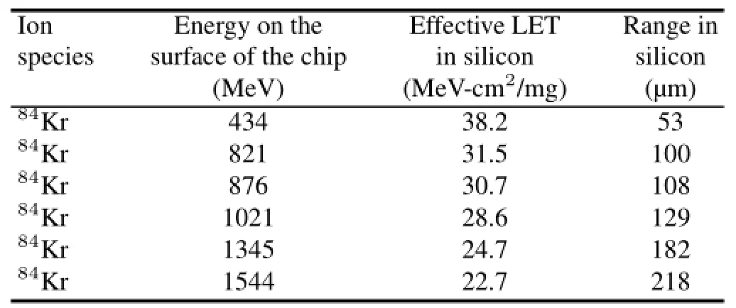
TABLE 1.LET values used in testing
No latch-up event was observed below the effective LET of 22.7MeV-cm2/mg with the total dose greater than 1×10⁷ions/cm2.Three chips were used to con fi rm this phenomenon and come to a conclusion that the LET threshold was between 22.7MeV-cm2/mg and 24.7MeV-cm2/mg.A Weibull curve is fi tted in Fig.4 to indicate that the saturated cross section is close to 2.0×10⁻⁴cm2/device.
When latch-up occurred,the currents of DVDD,DVSS and AVSS suddenly increased and the currents of AVDD and GND were almost stable.Current increased in DVDD was equal to the sum of currents increased in DVSS and AVSS.In addition, without powering off the chip during irradiation exposure,a phenomenon that the SEL current increased step by step wasfound,which could be speculated that multiple local latch-up events were triggered.
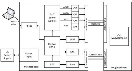
Fig.2.Block diagram of the VA32 test setup.
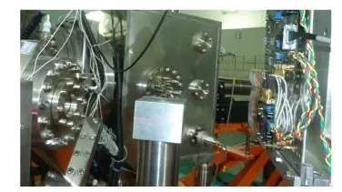
Fig.3.(Color online)SEE test at HIRFL.
SEU monitoring was always ongoing during power-up. During the entire irradiation experiment,no SEU event was observed before SEL occurred.
V.TID TEST AND RESULTS
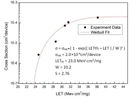
Fig.4.(Color online)Cross section versus the effective LET for SEL.
Two60Co gamma sources with an activity order of about 104Curie were used for the TID test.To minimize dose enhancement effects caused by low-energy,scattered radiation,the daughterboard was enclosed in a Pb/Al container of 2.0mm Pb with an inner lining of 1.0mm Al,and an in-situ radiation test was performed[12,13].To assure the insensitivity and stability of the test setup,the daughterboard was tested before and after each irradiation exposure through a golden chip which kept away from irradiation,and the motherboard was placed 4 meters away from radiation source and behind the concrete wall with a thickness of 1 meter.Three VA32 chips were irradiated up to 25Krad(Si)with a dose rate of 5.6rad/s. Annealling at 100◦C for 168 hours was done after irradiation exposure.The experiment result showed that no evident degradation was found.Since different dose rate may have different effects on the chip,the study of the relation between VA32 electrical characteristics and accumulated dose was conducted in further.Three more chips were irradiated up to 370Krad(Si) with a dose rate of 12.9rad/s.Room temperature annealing for 168 hours and annealing at 100◦C for 168 hours were done insuccession.
Figure 5 shows the VA32 operating currents as a function of TID.When ionizing dose was greater than 55Krad(Si),IDVDDand IDVSSstarted to rise slowly.After 12 hours room temperature anneal,IDVDDand IDVSSreturned to normal value.IAVDDand IAVSSchanged little during the entire f l ow.
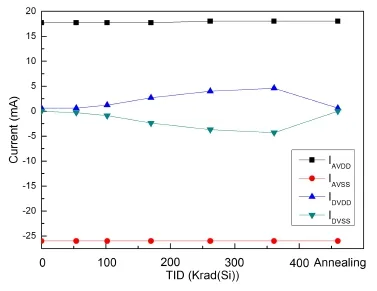
Fig.5.(Color online)Operating currents of VA32 in the irradiation fl ow.
Thepedestalsof32analogchannelsofVA32weremeasured during the test.For the circuits of 32 analog channels on one single chip are exactly the same,they have the similar trend of radiation response.Fig.6 shows pedestal degradation of the 4th,12th,20thand 28thchannel.The measured RMS noise of pedestal,which was the sum of VA32 and setup,was below 3fC during the test,which meant that no evident degradation of noise level was observed.
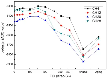
Fig.6.(Color online)Pedestal degradation.
The gain of VA32 was measured by the calibration charge in the range of−2.0pC to 16.0pC.The gain was linearly f i t in the range of 0 pC to 12.0pC.As shown in Fig.7,the gain decreased while dose was accumulating,which could be characterized by the slope,but the range of linear interval increased. Fig.8 shows the gain degradation of the chip.After room temperature anneal and accelerated ageing,the gain was slightly greater than pre-irradiation.
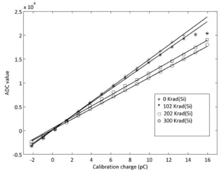
Fig.7.Linearity and range affected by TID.
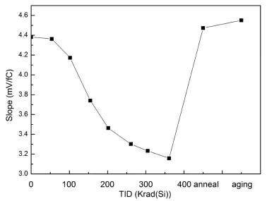
Fig.8.Gain degradation with TID.
VI.DISCUSSION
BGOcalorimeterneedsnearlyahundredVA32chips,which requires a serious consideration of radiation tolerance.
The VA32 is relatively sensitive to SEL because the LET threshold is around 23.0MeV-cm2/mg and lower than the design specif i cation,a current measurement and power protection circuit with fast response is suggested.There are at most 6 chips mounted on a front-end electronics board of the calorimeter.As observed in heavy-ion SEE test,the current of VA32 was between about 80mA to 170mA when the f i rst SEL occurred,which was about 3 to 6 times as much as the normaloperating current,that makes it feasible for up to 6 devices to share a current measurement and power protection circuit to simplify the design.
The values of 32-bit output shift register which were monitored to f i nd SEU were shifted out in readout operation during the irradiation.No SEU event was observed.The main reason is that the reset signal of the chip was activated before each readout operation,which would reset 32bit registers whether SEU event occurred or not.Besides,it took less than 50µs for each readout operation which was executed once per second in the heavy-ion test,which made it become a rare event when the ion hit the sensitive area.It comes to a conclusion that the output shift register is insensitive to SEU.
As reset avoids the SEU events from accumulating,even if SEU would happen to occur during readout operation in the front-end electronics,only one data packet would be affected as each packet is independent.Therefore,there is no need to use additional mitigation methods.Since it is not practical to run the test at a dose rate as low as space environment(from a few mrad/s to hundreds of mrad/s),the testing strategy is to irradiate the chip at a high dose rate for convenience.The test result showed that the electrical characteristics of VA32 kept stable when the dose was above 25Krad(Si),which was better than required.The chip functionality didn’t fail even the dose was greater than 350Krad(Si)and the electrical parameters almost recovered after room temperature annealing.The reason can probably be ascribed to the time dependent effect that degradation in electrical parameters caused by the growth of radiation trapped charge during irradiation for the high dose rate.
VII.CONCLUSION
The VA32HDR14.2 ASIC was experimentally validated to comply with the levels of radiation tolerance required by the DAMPE project.Both SEE and TID irradiation tests were performed.The chip is regarded to be relatively sensitive to SEL and protection methods must be adopted.The TID radiation result shows satisfactory radiation tolerance of the chip.
ACKNOWLEDGEMENTS
The SEE test in this paper was conducted at Heavy Ion Research Facility in Lanzhou(HIRFL)located at Institute of Modern Physics,Chinese Academy of Sciences(IMPCAS). The authors are grateful for the support of HIRFL team.The TID tests in this paper were conducted at University of Science and Technology of China(USTC)and National Institute of Metrology,China.
[1]Baker D N.Effects of hostile space weather on satellite operations,2011 IEEE International Symposium on Electromagnetic Compatibility(EMC).Rome,Aug.14–19,2011.
[2]Vampola A L.IEEE Trans Plasma Sci,2000,28:1831–1839.
[3]Barth J L,Dyer C S,Stassinopoulos E G.IEEE Trans Nucl Sci, 2003,50:466–382.
[4]Chang J.Journal of Engineering Studies,2010,2:95–99(in Chinese).
[5]Zhang Y L.PH.D.The Study of an EM Calorimeter for Searching Dark Matter in Space,University of Science and Technology of China,2011.
[6]ZhangYL,LiB,FengCQ,etal.ChinPhysC,2012,36:71–73.
[7]Feng C Q.PH.D.The Research on the Readout Electronics for the Calorimeter Detector of the Dark Matter Exploration Satellite,University of Science and Technology of China,2011.
[8]Guo J H,CAI M S,HU Y M,et al.Acta Astronomica Sinica, 2012,53:72–29(in Chinese).
[9]VA32HDR14.2 Datasheet,IDEAS Inc.
[10]EIA/JEDEC Standard.EIA/JESD57,Test Procedures for the Measurement of Single–Event Effects in Semiconductor Devices from Heavy Ion Irradiation,1996.
[11]ESCC Basic Specif i cation No.25100,Single Event Effects Test Method and Guidelines,2002.
[12]ESCC Basic Specif i cation No.22900,Total Dose Steady–state Irradiation Test Method,2007.
[13]US MIL–STD–883G Method 1019.7,Ionizing radiation(total dose)test procedure,2006.
10.13538/j.1001-8042/nst.25.010402
(Received October 11,2013;accepted in revised form November 27,2013;published online February 20,2014)
∗Supported by the Strategic Priority Research Program on Space Science,the Chinese Academy of Sciences(No.XDA04040202-4)
†Corresponding author,fengcq@ustc.edu.cn
猜你喜欢
山东文学(2022年4期)2022-10-29
安徽文学(2022年6期)2022-06-13
课外语文·中(2022年3期)2022-04-21
作文大王·低年级(2021年2期)2021-02-21
学生天地(2020年14期)2020-08-25
小读者之友(2019年6期)2019-09-10
莫愁(2019年3期)2019-02-22
莫愁·家教与成才(2019年1期)2019-01-24
今日重庆(2016年2期)2016-08-11
西部(2011年5期)2011-08-15
 Nuclear Science and Techniques2014年1期
- Nuclear Science and Techniques的其它文章
- Feasibility study on optical vortex generation at Shanghai deep ultraviolet free-electron laser∗
- Lattice design and optimization of the SSRF storage ring with super-bends
- Temperature and carrier-density dependent excitonic absorption spectra of semiconductor quantum wires∗
- Bromate formation in bromide-containing waters irradiated by gamma rays∗
- Adsorption behavior of uranyl ions onto amino-type adsorbents prepared by radiation-inducedgraft copolymerization∗
- A 16-Channel high-resolution time and charge measurement module for the external target experiment in the CSR of HIRFL∗