
Sub-stochiometric MoOx by radio-frequency magnetron sputtering as hole-selective passivating contacts for silicon heterojunction solar cells
2022-09-24 08:04XiufangYang杨秀芳ShengshengZhao赵生盛QianHuang黄茜CaoYu郁超JiakaiZhou周佳凯XiaoningLiu柳晓宁XianglinSu苏祥林YingZhao赵颖andGuofuHou侯国付
Chinese Physics B 2022年9期
关键词:祥林
Xiufang Yang(杨秀芳) Shengsheng Zhao(赵生盛) Qian Huang(黄茜) Cao Yu(郁超)Jiakai Zhou(周佳凯) Xiaoning Liu(柳晓宁) Xianglin Su(苏祥林)Ying Zhao(赵颖) and Guofu Hou(侯国付)
1Institute of Photoelectronic Thin Film Devices and Technology of Nankai University,Tianjin 300350,China
2Key Laboratory of Photoelectronic Thin Film Devices and Technology of Tianjin,Tianjin 300350,China
3Collaborative Innovation Center of Chemical Science and Engineering(Tianjin),Tianjin 300072,China
4Engineering Center of Thin Film Photoelectronic Technology of Ministry of Education,Tianjin 300350,China
5Suzhou Maxwell Automation Equipment Co. Ltd,Suzhou 215299,China
Keywords: radio-frequency magnetron sputtering,silicon heterojunction(SHJ)solar cell,MoOx,hole transport layer
1. Introduction
In the past decades, amorphous/crystalline silicon heterojunction solar cells have been one of the most promising candidates for low-cost and highly-efficient solar cells.[1,2]Intrinsically hydrogenated amorphous silicon (a-Si:H(i)) films have been widely adopted as the passivating layer and emitting layer in the silicon heterojunction(SHJ)solar cells,which effectively enhance the open circuit voltage(Voc). Kaneka Co.Ltd has reported heterojunction interdigitated back contact(HJ-IBC) cell with the record efficiency of 26.63%.[3]However, the unavoidable parasitic absorption caused by a-Si:H passivating layer and emitting layer is considered as the main limitation to further improve the SHJ device performance. In order to get p-type or n-type a-Si:H layers, highly toxic PH3or B2H6dopants are usually adopted. In addition,the heavily doped carrier selective layer (n+, p+) leads to serious carrier combination. Therefore, hydrogenated amorphous silicon alloyed with carbon,oxygen and nitrogen etc. are used to obtain wide bandgap silicon films to partially decrease the parasitic absorption.[4-6]Many researchers have tried to adjust the work function of the n+/p+layers by optimizing doping techniques to achieve better band matching effects with c-Si.[7-9]Other studies have proven that it is a more convenient and effective way to insert a buffer layer with high work function to further extract carriers at the c-Si interface.[10-14]
Recently, novel carrier-selective passivating materials have been extensively developed, especially nonstoichiometric transition metal oxides with high work function including WOx(x <3),[7]V2Ox(x <5),[15,16]CrOx(x <3)[17,18]and MoOx(x <3).[7,19-21]Among them, MoOxhas attracted extensive attention as a hole selective transport layer (HTL) in organic solar cells and undoped asymmetric heterogeneous contact (DASH) silicon solar cells due to its high work function and unique electrical and optical properties.[21-25]The combination of high work function MoOxwith lightly doped c-Si(n) substrate will lead to upward band bending at the c-Si interface, and the Fermi level of MoOxclose to the valence band of c-Si absorber, forming a favorable level alignment for band to band (B2B) hole transport.[26-28]
Various deposition techniques such as thermal evaporation,[29]electron beam evaporation,[30]pulsed laser deposition,[31]and sputtering[32-35]and sol-gel process[36]were employed for the growth of MoOxfilms. Compared with the traditional coating technology, magnetron sputtered films have stronger adhesion with the substrate,and it is more convenient to fabricate the films with high melting point materials. It is easy to control the composition of the films by varying the target material and to realize reactive sputtering,which can be more convenient for plating a variety of films.RF sputtered is preferred to other deposition methods for large area and good reproducibility, too. Recently, several groups reported MoOxfilms by reactive sputtering from the Mo metal target and applying MoOxfilms as hole-selective contacts in SHJ cells.Boccardet al.observed a barrier for hole extraction due to the stoichiometric issues. It has been demonstrated that TMOs thin films with low average oxidation state present better transport properties,while moderate carrier selectivity.[37]Bivouret al.demonstrated the suitability of sputtered MoOxthin film as a carrier-selective contact for the n-type silicon(n-Si) wafer, and highlighted the importance of higher work function MoOxfilm to improve the hole-selectivity due to c-Si upward band bending at the n-Si/MoOxinterface.[38]So far,several groups have reported MoOx-based SHJ solar cells with efficiencies up to 22% or even the highest one of 23.5%.[39]In most cases the evaporation method is adopted to deposit MoOxfilms. Truth to be told that the evaporation is not a popular method in industrial production, at least not as good as the sputtering one.It is worth mentioning that sputtered MoOxfilms as HTL for c-Si SHJ solar cell has not been reported with efficiency over than 15%up to now.

Fig.1. Schematic structures of SHJ solar cells with MoOx as buffer layer(a)and hole transport layer(b),respectively.
In this experiment,we demonstrated magnetron sputtered MoOxfilms and applications in SHJ solar cells. The results show that the MoOxfilm as a buffer layer effectively improve the SHJ device efficiency to 19.1%. Meanwhile, we demonstrated that MoOxcan replace p-type a-Si:H emitting layer as a hole selective transport layer, resulting in a conversion efficiency of 17.5%,which is the highest one for the MoOxfilm as HTL by RF sputtering,to the best of our knowledge.
2. Experimental details
2.1. Film and device fabrication
All the solar cells were fabricated on CZ n-type c-Si(5 cm×5 cm, 1-3 Ω, 180µm)substrates. A stack composed of a-Si:H(i)/a-Si:H(n or p) was deposited at the both sides by plasma enhanced chemical vapor deposition (PECVD) at 300°C on all substrates. The MoOxfilms were deposited on n-type c-Si and Eagle glass substrates by 13.56 MHz RF magnetron sputtering from a MoO3(>99.95%)target. MoOxsputtering process was done in a vacuum chamber(base pressure before deposition~2×10⁻⁴Pa), from a stoichiometric MoO3target at 160°C, with argon flow of 60 sccm,working pressure at 2×10⁻⁴Pa and RF power density with 1.75 W/cm2. In order to ensure the same experimental conditions, the target was pre-sputtered in argon for about 30 minutes before the formal deposition. Then,ITO films with thickness about 80-100 nm were prepared on passivated selective contacts by using thermal evaporated method. Finally,800 nm thick Ag+Al gridlines were deposited on the front surface by using thermal evaporated,and Al electrodes of the same thickness were deposited on the rear field. In our work,the performances of solar cells with MoOxfilm as buffer layer and HTL are analyzed, respectively. The schematic structures of fabricated solar cells are shown in Fig.1. During the test,a reticle was used to block the redundant part,and the illumination area was 1 cm×1 cm.
2.2. Film and device characteristics
Top-view of scanning electron microscopy (SEM) images were characterized by Jeol JSM-6700F scanning electron microscope. The quasi-steady state photoconductivity decay(QSSPC) method was used to measure the minority carrier lifetime of the samples by the WCT-120 minority carrier lifetime tester from Sinton Instruments company. The x-ray photoelectron spectroscopy (XPS) and ultraviolet photoelectron spectroscopy (UPS) measurements of the MoOxfilms coated on indium tin oxides(ITO)were performed in an ESCALAB 250Xi. Finally,the solar cells were tested with a Wacom solar simulator(WXS-156S-L2,AM1.5GMM)under the room temperature of 25°C,standard spectrum AM1.5 and power density of 100 mW/cm2. The quantum efficiency of the devices was tested by the QEX10 quantum efficiency system from PV Measurements company.
3. Results and discussion
3.1. Surface morphology of MoOx film
The MoOxfilms were prepared by magnetron sputtering process of specific target and deposited on a-Si:H(i)/c-Si with film thickness of 5 nm and 30 nm, respectively. Morphology of MoOxfilms is a crucial factor to affect the performance of as-fabricated devices. The SEM images of MoOxfilms reveal uniform and dense surface morphologies, where no obvious cracks can be observed for the sample,indicating the positive effect on the devices (Figs. 2(a) and 2(b)). Moreover, it can be seen that an ultrathin MoOxfilm can fully cover the pyramidally textured surface. Fortunately, no cracks appeared at the bottoms of the pyramids when the MoOxfilm thickness increased to 30 nm.
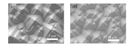
Fig.2. SEM images of(a)5 nm MoOx and(b)30 nm MoOx films. All scale bars are 5µm.
3.2. The passivation quality of sputtered MoOx layer
As we all know,sputtered damage is inevitable in the thin film fabrication process. When the precursors migrate through the deposition chamber and reach the c-Si substrate,the sputtered particle groups or atoms from the target usually have enough energy to damage passivation layer. Therefore, this has prompted scientists to develop new techniques to circumvent the bombardment on passivation layer during sputtering process.Studies have shown that environmental annealing can effectively change the stoichiometric ratio of Mo/O ratio and reduce the defect density states in MoOxfilms.[24]For samples subjected to ion bombardment,annealing is an effective way to restore the passivation quality. In general,the minority carrier lifetime was used to characterize the passivation performance.Minority carrier lifetime as a function of minority carrier density of samples without MoOx,with as-sputtered 5 nm MoOxand with post-annealed 5 nm MoOxwere measured and the results are shown in Fig. 3. For the sample with only 5 nm a-Si:H(i) passivating layer, the minority carrier lifetime is as high as 3911 µs at minority carrier density of 1×1015cm-3and implied open circuit voltage(iVoc)of 725 mV.Then 5 nm MoOxwere subsequently sputtered, which dramatically decrease the minority carrier lifetime to 2119 µs and iVocof 710 mV. The following post-annealing with temperature of 200°C and process duration of 60 min was performed on the sample,the minority carrier lifetime was 3752µs and iVocof 721 mV, which is nearly as good as the original one. Since the thermal annealing can almost totally recover the passivation quality, the above results demonstrate the feasibility of application of sputtered MoOxinto SHJ solar cells to a large extent.
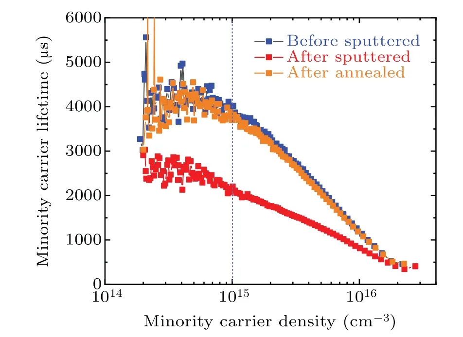
Fig. 3. Minority carrier lifetime as a function of minority carrier density of samples without MoOx,with as-sputtered 5 nm MoOx and with post-annealed 5 nm MoOx.
3.3. The characteristics of MoOx films
Affected by the preparation method and deposition conditions,the as-deposited transition metal oxide film is usually non-stoichiometric. The chemical state,element composition and electronic properties determine the work function of the transition metal oxides. Furthermore,the energy level matching of each functional layer is an important prerequisite to get better device performance. XPS was used to analyze the as-sputtered and post-annealed MoOxfilms. The corresponding Mo 3d and O 1s XPS spectra are shown in Fig. 4, while the composition and binding energy positions of the oxidation state are listed in Table 1. As we all know that even if a fully stoichiometric MoO3target is adopted,it is still impossible to get fully stoichiometric MoO3films by the sputtering process.Usually, MoOxfilms were obtained withxin the range from two to three, which mean that both Mo6+and Mo5+oxidation states exist in the films. For the as-sputtered MoOxfilm in our experiments,the O/Mo ratio was calculated to be~2.83.The deconvolution of the spectra was calibrated by referencing to the well-known adventitious hydrocarbon C 1s peak at~284.8 eV. The spectra of Mo 3d core level energy was deconvoluted into two shoulders positioned at~232.6 eV and~231.1 eV, which correspond to Mo6+and Mo5+oxidation state with the Mo 3d 5/2 peak,respectively(Fig.4(a)). Similarly,another doublet splitting represents the Mo6+oxidation state with the Mo 3d 3/2 peak centered at~235.8 eV and the Mo5+oxidation state with the Mo 3d 3/2 at~234.5 eV. For the post-annealed MoOxfilm(Fig.4(b)),the annealing process results with increased oxygen concentration in the film, were also revealed in the O 1s XPS (Figs. 4(c) and 4(d)). The Mo 3d curve consists of two sub-curves centered at~232.9 eV and at~231.8 eV,which represent the Mo6+and Mo5+oxidation state with the Mo 3d 5/2,respectively. On the contrary,shoulders peaked at~236.0 eV and at~234.9 eV represent the Mo6+and Mo5+oxidation state with the Mo 3d 3/2, respectively. (ΔB.E.=E(Mo3d3/2)-E(Mo3d5/2)=3.15 eV).

Fig.4. XPS analysis of as-sputtered and annealed MoOx films: (a)as-sputtered Mo 3d,(b)annealed Mo 3d,(c)as-sputtered O 1s,(d)annealed O 1s,respectively.
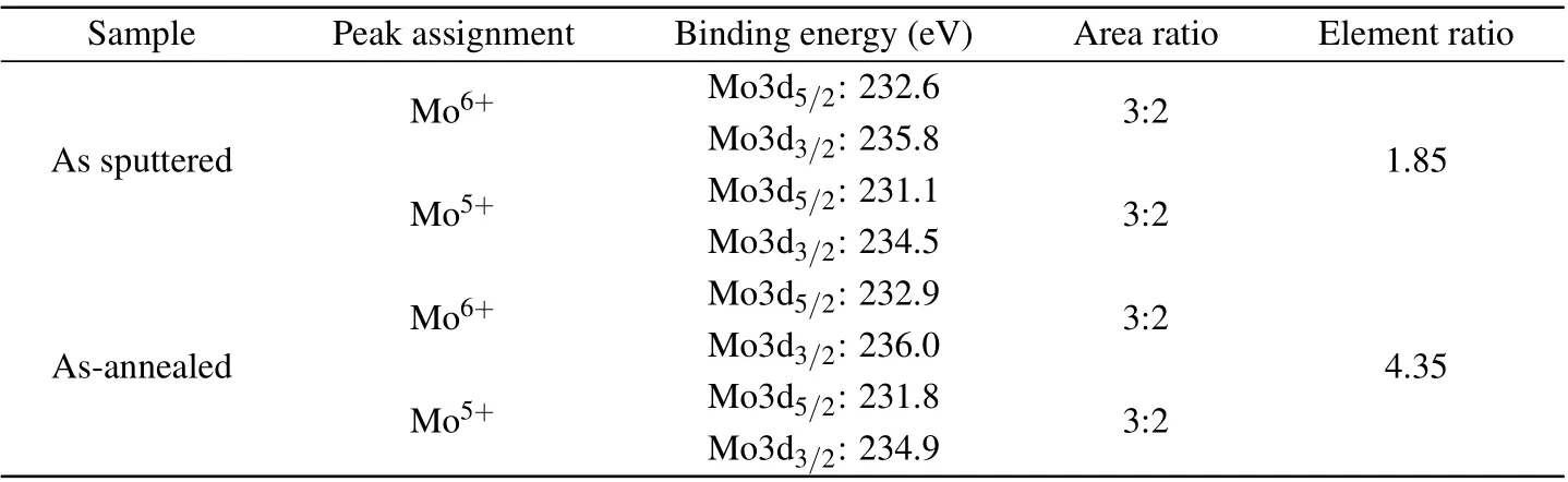
Table 1. Peak positions of the XPS spectra of as-sputtered and annealed MoOx films.
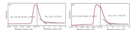
Fig.5. UPS analysis of(a)the as-sputtered MoOx film and(b)the post-annealed MoOx film.
To further confirm the influence of the annealed atmosphere on the work function and oxygen vacancies of the MoOxfilms,UPS measurements were performed for the corresponding films,as shown in Fig.5. Similar to the XPS results,the UPS spectra showed an increase of the oxygen concentration in the film during annealing process. The as-sputtered MoOxsample demonstrated a work function of 4.88 eV,while the work function of the post-annealed MoOxincreased to a much higher value of 5.16 eV, which was also much higher than that of transparent conductive oxide(TCO)(4.7 eV).[26]From the above-mentioned XPS and UPS results, the postannealing process proved to be an effective method to control the oxygen vacancies and the existence of the Mo5+and/or Mo6+cation in the MoOxfilm,as well as to increase the work function.
3.4. MoOx as a buffer layer between p-a-Si:H/ITO interface
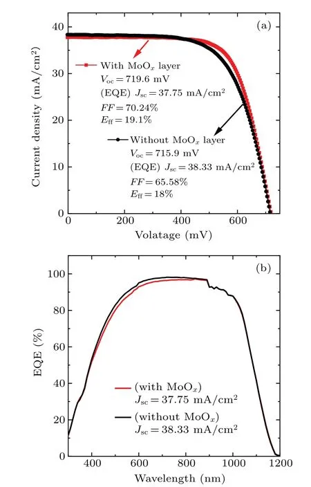
Fig.6. Comparison of conventional SHJ solar cells with or without sputtered 5 nm MoOx buffer layer with(a)J-V curves,(b)EQE spectra.
In this section, the above-mentioned MoOxfilms were applied into SHJ solar cells to study their influence on device performance. In the first step, the MoOxfilm was inserted as a buffer layer between TCO and p-type a-Si:H emitting layer in a conventional SHJ cell. As can be seen from Fig.6(a),the conversion efficiency of the reference SHJ solar cell is 18%withVocof 715.9 mV,Jscof 38.33 mA/cm2andFFof 65.58%.On the contrary, the insertion of 5 nm MoOxbetween TCO and a-Si:H(p)can effectively increaseVocup to 719.6 mV andFFup to 70.24%, respectively. However, theJscslightly decreased to 37.75 mA/cm2,which can be contributed to the parasitic absorption of MoOxbecause of its relatively low optical transmittance.It can be seen from Fig.6(b)that although these two solar cells behave very similar to EQE spectral responses in the infrared band, the EQE spectral response in the visible region of the reference SHJ solar cell is obviously higher than that of the device with MoOxbuffer layer. Finally, the conversion efficiency was improved to 19.1%, which can be attributed to the decrease of contact barrier and improvement of energy level matching between TCO and a-Si:H(p) interface by inserting the MoOxbuffer layer.
3.5. MoOx as the hole selective transport layer

Fig. 7. Contact resistivity ρc measurements of MoOx-based contacts to ntype c-Si. (a) A series of I-V measurements of the samples with optimal thickness of MoOx films,and(b)the ρc with different thickness. Schematics of the contact resistivity test structure samples is included in inset.
In the following step, the MoOxfilm as a hole selective transport layer was applied into a SHJ solar cell to replace the a-Si:H(p) emitting layer. To evaluate the hole-selective contact behavior of the i-a-Si:H/MoOx, the contact resistivityρcwas measured by using the method devised by Cox and Strack.A series of current-voltage(I-V)measurements of the samples with optimal thickness of MoOxfilms and theρcwith different thickness are presented in Fig.7,with the test structure in the inset. As can be seen in Fig.7(a),the sample with Ag directly deposited MoOxexhibited Schottky contacts for different sizes area pads. We determined the extracted contact resistivityρcfor the structure with n-Si/a-Si:H/MoOx/Ag to be 0.8 Ω·cm2.
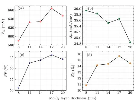
Fig.8. The influence of MoOx thickness on J-V output parameters(a)Voc,(b)Jsc,(c)FF and(d)Eff.
The influence of MoOxthickness onJ-Vparameters of SHJ solar cells with MoOxas the hole selective layers are shown in Fig. 8. In fact, the increase of MoOxthickness has two opposite effects: the positive one is to improve the passivating quality and built-in electric field because of fully covered c-Si surface by thick enough MoOxlayer,while the negative one is to increase the series resistance and parasitic absorption. The increase of series resistance would hinder the carrier transport and then lead toVocandFFdecrease,while the increase of parasitic absorption will result inJscdecrease.The results in Fig. 8 indicate that with the increase of MoOxthickness theJscmonotonically decrease. On the contrary,theVocandFFdemonstrate peak values when the MoOxthickness is 17 nm, which can be contributed by balancing the abovementioned positive and negative effects. Eventually, a 17 nm MoOxfilm prepared by sputtering method is successfully used as the hole transport layer in SHJ solar cell, and the conversion efficiency reach the maximum value of 15.69%.Based on the above results,the MoOxfilms with sufficient thickness are able to obtain good passivating quality and build a high built-in electric field to achieve carrier selectivity. In order to further improve the passivation effect, we try to increase the thickness of the a-Si:H(i)passivation layer and reduce the deposition temperature of thermal evaporated ITO films. Although the thicker a-Si:H layer limiting the short-circuit current density, theVocandFFare significantly improved. Finally, a champion conversion efficiency of 17.5%withVocof 711 mV,Jscof 32.8 mA/cm2andFFof 74.9% is currently obtained,as shown in Fig. 9. As mentioned above, a relatively thick(17 nm) MoOxfilm results in a decrease ofJsc. This is consistent with the optical results,where 17-nm-thick MoOxfilm demonstrated the poor optical transmittance around 75%(the red curve)in the visible spectrum region,as shown in Fig.10.We infer that the lower transmittance may be related to the ion bombardment on MoOxfilms and deteriorate the film quality during the sputtering process. Further optimization will be carried out including pre-treatment, post-annealing in various gaseous environments,mesh electrode with bias voltage,etc. to control the ion damage on the films and interfaces and then ultimately improve the device performance. Moreover,oxygen vacancies in TMOs appear during film deposition or exposure to air.[28]According to the UPS test results,the factors affecting the work function of the oxygen concentration in the metal oxide should be taken into consideration. The main factors that reduce the device performance with the sputtered MoOxfilm require further intensive research.
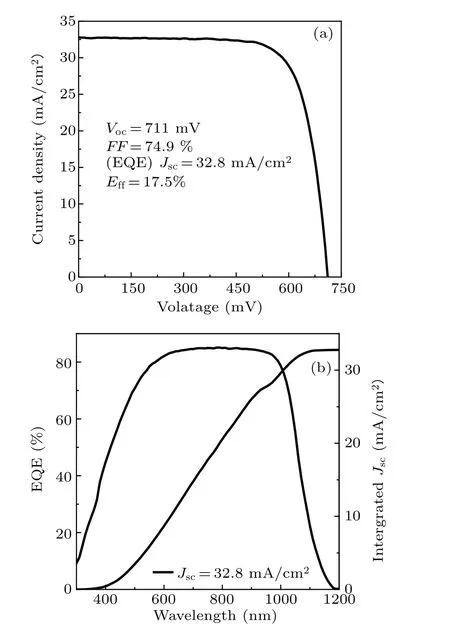
Fig.9. The champion SHJ solar cell with 17 nm MoOx hole transport layer: (a)J-V curve,(b)EQE spectra.

Fig. 10. The transmittance of MoOx films prepared under various RF sputtering power.
4. Conclusion
The effects of MoOxas buffer layer and hole transport layer on the performance of SHJ solar cells were investigated.The results show that the high work function of MoOxlayer enable to significantly improve the performance of solar cells.By inserting a 5 nm MoOxbuffer layer between a-Si:H(p)/ITO interface result in an efficiency of 19.1%withVocof 719.6 mV,Jscof 37.75 mA/cm2, andFFof 70.24%. In addition, the best conversion efficiency of 17.5% andFFof 74.9% were obtained by using 17 nm MoOxfilm as the hole selective layer to replace the p-type a-Si:H emitting layer. These results in this manuscript confirm the feasibility of a sputtering process of MoOxfilms and their application in SHJ solar cells. Further optimization of magnetron sputtered MoOxis urgently deserved to improve SHJ solar cell performance.
Acknowledgements
Project supported by the National Natural Science Foundation of China (Grant No. 62074084), the National Key Research and Development Program of China (Grant No.2018YFB1500402),and Key Research and Development Program of Hebei Province,China(Grant No.20314303D).
猜你喜欢
铁军(2022年7期)2022-07-08
南风·中旬(2021年2期)2021-07-23
中国纤检(2020年5期)2020-11-25
求学·理科版(2020年12期)2020-03-03
东西南北(2019年20期)2019-12-12
求学·理科版(2019年9期)2019-09-28
东西南北(2019年22期)2019-01-03
高中生·天天向上(2018年2期)2018-04-14
中华奇石(2016年10期)2016-11-17
周末·校园文学(2015年31期)2015-12-10
- Chinese Physics B的其它文章
- Characterizing entanglement in non-Hermitian chaotic systems via out-of-time ordered correlators
- Steering quantum nonlocalities of quantum dot system suffering from decoherence
- Probabilistic quantum teleportation of shared quantum secret
- Spin–orbit coupling adjusting topological superfluid of mass-imbalanced Fermi gas
- Improvement of a continuous-variable measurement-device-independent quantum key distribution system via quantum scissors
- An overview of quantum error mitigation formulas