
双腔室分子束外延复合体在III-V族和II-VI族半导体异质结生长中的应用
2010-03-23 03:44AlexeevBaranovPetrovSedovaSorokin
电子工业专用设备 2010年10期
A.Alexeev,D.Baranov,S.Petrov,I.Sedova,S.Sorokin
(1.SemiTEq JSC;2.Ioffe Physical Technical Institute of RAS)
1 Materials and Methods
The appearance of the commercial compact semiconductor lasers emitting in the green spectrum range (500~550nm)will open new possibilities for creating optical devices of the new generation,such as full-color optical displays,pico-projectors compatible with mobile phones and laptop systems,laser projection television,all-weather navigation and radar systems,high-quality color printing devices and etc.Novelty and urgency of this theme are confirmed by the absence of semiconductor lasers with operating wavelength in the green spectral range on the domestic and world markets.Today the only technological possibility of overlapping the green spectral range by low-threshold lasers could be achieved by widegap II-IV semiconductors application[1,2].In this case,to obtain low-defect density II-IV heterostructures on GaAs wafers it's necessary to use GaAs buffer layers that are III-V semiconductor compounds.The basic method of creating III-V and II-IV nanoheterostructures including heterovalent interface is a molecular-beam epitaxy(MBE).
2 Result and discussing:
To create the equipment for III-V and II-VI nanoheterostructures growth it's necessary to consider high requirements for MBE system:
*only two-growth chamber version because materials for III-V/II-VI compound growth are doping impurities for each other;
* UHV transport allowing samplestransfer through transmission chamber without contamination of surface and with conservation of required surface reconstruction;
*maximum cleanness of residual atmosphere in vacuum chambers;
*reliable operation of molecular sources shutters;
*stable operation of the materials sources and the sample heater at rather low operating temperatures(2000~4000℃).

Fig.1 Two-Growth chamber MBE complex for hybrid III-V and II-IV nanoheterostructures growth
The prototype of STE3526 MBE complex for III-V and II-VI nanoheterostructures growth(Fig.1)was created in"Semiconductor Technologies and Equipment"Joint Stock Company (SemiTEq JSC)and today is operated in Ioffe Physical Technical institute of the Russian Academy of Sciences.The basic direction–III-V and II-VI growth laser nanoheterostructure for active elements of electron beam pumped semiconductor lasers and injection laser converters of a green spectral range.For today the following results of complex's possibilities are shown:
* Test heterostructures with 10 nm Al-GaAs/GaAs quantum wells(QWs)with photoluminescence maximum intensity at energy 1,54 eV and full width at half maximum(FWHM)less than 6 MeV(at 77 К)are received that shows the high QW structural and optical perfection and reflecting high cleanness of residual atmosphere in А3В5 chamber and extremely high quality of molecular beam sources and the manipulator of a substrate.
*The universal technique of determination of true value of substrate temperature with error no more than 5℃in operating range 250~350℃based on experimentally defined dependence of thermocouple indications which control substrate holder temperature on the heater power and experimentally defined dependence of the factor of incorporation of sulfur in ZnMgSSe system from temperature is developed[3].
*The technique of GaAs substrate preparation before growth and ZnSe growth initiation mode leading to 2D growth mechanism of ZnSe and providing low treading dislocation and stacking fault density in А2В6 nanoheterostructures is developed.
*Test heterostructures Cd(Zn)Se/ZnMgSSe on GaAs buffer layers for lasers of the green range showing photoluminescence intensity at wave length of 530nm several times above in comparison with the similar structures grown in MBE system of the previous generation are received(Fig.2).
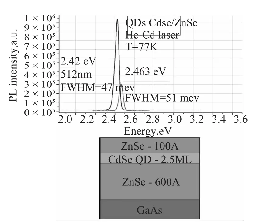
Fig.2 Photoluminescence spectrum of test structures on GaAs buffer layer with quantum dots CdSe/ZnSe.STE3526 complex's result(blue line),MBE system of previous generation result(red line).Test heterostructure's scheme.
Thus,taking into account modern requirements of technological equipment level,this MBE complex was specially designed to solve advanced problems of modern nanophotonics and nanoelectronics.
[1]E.Kato,H.Noguchi,M.Nagai,H.Okuyama,S.Kijima,A.Ishibashi,Electron.Lett.34,282(1998)[Z].
[2]S.V.Ivanov,ZnSe-based lasers and laser diode converters,16th Int.Conf.on MBE(MBE 2010),22-27 August,Berlin(2010)(invited paper)[Z].
[3]S.V.Ivanov,S.V.Sorokin,P.S.Kop'ev,J.R.Kim,H.D.JungandH.S.Park,J.CrystalGrowth159,16(1996)[Z].
猜你喜欢
中国病理生理杂志(2018年6期)2018-01-22
中国劳动关系学院学报(2016年3期)2016-09-26
意林(2016年13期)2016-08-18
唐山文学(2016年11期)2016-03-20
云南师范大学学报(自然科学版)(2015年5期)2015-12-26
原子与分子物理学报(2015年1期)2015-11-24
中国科技信息(2015年24期)2015-11-07
中央民族大学学报(自然科学版)(2015年2期)2015-06-09
物理实验(2015年10期)2015-02-28
公务员文萃(2013年5期)2013-03-11

- 电子工业专用设备的其它文章
- 3D互连中光刻与晶圆级键合技术面临的挑战,趋势及解决方案