
一维带状SnO2的电子传输性能
2012-11-30 10:57李晓宁白守礼杨文胜陈霭璠孙丽娜张敬波
物理化学学报 2012年7期
李晓宁 白守礼 杨文胜 陈霭璠 孙丽娜 林 原 张敬波,3,*
(1北京化工大学,化工资源有效利用国家重点实验室,北京100029;2中国科学院化学研究所,北京分子科学国家实验室,北京100190;3天津师范大学,天津市功能分子结构与性能重点实验室,天津300387)
一维带状SnO2的电子传输性能
李晓宁1,2白守礼1,*杨文胜1陈霭璠1孙丽娜1林 原2张敬波2,3,*
(1北京化工大学,化工资源有效利用国家重点实验室,北京100029;2中国科学院化学研究所,北京分子科学国家实验室,北京100190;3天津师范大学,天津市功能分子结构与性能重点实验室,天津300387)
采用水辅助化学气相沉积法制备了结晶性好的一维带状SnO2.分别以小粒径锡粉和金修饰的小粒径锡粉作为反应原料制得带宽度不同的带状SnO2,小粒径锡粉作为反应原料能提高带状SnO2的产率.将所得SnO2带和SnO2纳米颗粒按不同比例混合配制成胶体,采用刮涂法制备含不同比例纳米颗粒和纳米带的复合SnO2薄膜并组装染料敏化太阳能电池(DSSCs)来评价带状SnO2的电子输运性能.组装的太阳能电池表现出与复合纳晶薄膜中一维SnO2带的带宽度和所含比例密切相关的光电性能.通过强度调制光电流谱的测量确定复合SnO2薄膜的电子传输速率,并进一步分析一维材料所具有的良好电子传输性能对光电流增加的贡献.因为一维SnO2带在复合纳晶薄膜中作为电子输运的快速通道可以加快电子的输运速度,所以以适宜的比例添加具有合适宽度的一维SnO2带可以明显提高太阳能电池的光电性能.
二氧化锡一维带状结构;电子传输;复合纳晶薄膜;染料敏化太阳能电池;光电性能
1 Introduction
Since OʹRegan and Grätzel1firstly reported dye-sensitized solar cell(DSSC)in 1991,it has been certificated as an efficient device for solar energy conversion.After intensive research of two decades,it still suffers from a relatively lower conversion efficiency.2-4The photogenerated electron transport processes in the semiconductor nanocrystalline thin film electrode are thought to essentially affect the conversion efficiency of DSSCs,which depends on the nature and morphology of nanocrystalline semiconductor oxides.5-9
Recently,one-dimensional(1D)structures,such as wires, rods,belts,and tubes,have become a research focus owing to their unique applications in mesoscopic physics and fabrication of nanoscale devices.10,11It is generally accepted that 1D structure provides a good system to investigate the dependence of electrical and thermal transport or mechanical properties on the dimensionality and size reduction.121D structure has a relatively small amount of grain boundaries,especially the well-crystallized structures,can reduce the grain boundary effect and provide a fast electron transport.13-15The recombination rate in TiO2nanotubes has been found to be 10 times slower than that in nanoparticles.16In 2006,Suzuki et al.17reported that a partially nanowire-structured TiO2electrode(TiO2nanoparticle/nanowire composite electrode)promises for high-performance DSSCs,because it offers possible electron transport paths without losing high surface area.They also improved the efficiency of DSSCs using well-crystallized TiO2anatase nanowires instead of TiO2nanowires with a number of structural defects,which indicates that well-crystallized TiO2anatase nanowires have better electron transport ability.18
Tin oxide(SnO2),a typical n-type semiconductor with a 3.6 eV band gap,is one of the most important and extensively used metal oxide materials for conducting electrodes of solar cells due to its high visible optical transparent property.And some researchers are trying to replace TiO2with SnO2nanomaterials to prepare the working electrode of DSSCs.19-21
In this paper,we synthesized the well-crystallized 1D structural SnO2belts with different widths in high yield by the water-assisted chemical vapour deposition(CVD)method at atmospheric pressure.And we tested the conversion efficiency of DSSCs by the incorporation of 1D structural SnO2belts in different percentages to photoelectrodes.The intensity modulated photocurrent spectroscopy(IMPS)was employed to investigate the electron transport process in the composite nanocrystalline film on the mode of DSSCs.The effects of structural SnO2belts with the different widths and incorporation amounts in the composite thin film on the photovoltaic performance were also discussed.
2 Experimental
All chemicals are analytic grade and were used as received. The SnO2belts were in situ grown in the ceramic boat containing pure Sn powder(100 mesh,99.9%,Alfa Aesar)or Au-modified Sn powder via a simple water-assisted CVD with water vapor as the oxidizer,which was introduced to the reaction region in a level tube furnace(Tianjin Zhonghuan Experiment Electric Stove Co.,Ltd.)by N2(99.999%).In a typical waterassisted CVD process,distilled water held with a ceramic boat was placed at 39 cm away from the center of the tube furnace. The tube furnace was first heated up to the set temperature (1050°C for the pure Sn powder and 850°C for the Au-modified Sn powder)under a heating rate of 10°C·min-1and then kept at the set temperature for 1 h.The N2gas at the rate of 80 cm3·min-1for the pure Sn powder or 50 cm3·min-1for the Au-modified Sn powder was introduced into the quartz tube during the heating process.When the furnace reached the set temperature,the ceramic boat with 0.3 g Sn powder was pushed into the heat center.After the reaction,the furnace was cooled to the room temperature in the N2atmosphere.The cotton-like products were formed to be full of the ceramic boat. The morphology of 1D structural SnO2was observed on an S-4800 field emission scanning microscope(FESEM),and a Tecnai G2 F20 U-TWIN high-resolution transmission electron microscope(HRTEM).X-ray diffraction pattern(XRD)of belts was measured with Riguku D/max 2500 using Cu Kαradiation.
SnO2electrodes were fabricated by the mixture of the 1D structural SnO2belts and commercial SnO2nanoparticles(99.99%, 20-70 nm,Aladdin Chemistry Co.,Ltd.)with mixing ratios of 20%,50%,80%,and 100%(w)(mass fractions of belts).A total of 0.2 g of mixture was ground mechanically in 0.02 mL of acethylacetone.A little surfactant(Triton X-100)was added to facilitate spreading of the paste on the substrate.The obtained colloidal paste was coated on fluorine-doped SnO2conducting glass(FTO,20 Ω·□-1,Hake New Energy Co.,Ltd.,Harbin)by the doctor-blade method.The SnO2films were sintered at 450 °C for 30 min in air,and then were soaked in 0.5 mmol·L-1ethanol solution of Ru(dcbpy)2(NCS)2(dcbpy:2,2ʹ-bipyridine 4, 4ʹ-dicarboxylic acid)(N3,Solaronix)for 24 h.The dye loading amount was determined by dissolving a known area of the film into a known volume of NaOH solution(0.1 mol·L-1)and measuring its absorption spectrum with UV(Labtech,UV 2000) spectrometer.The redox electrolyte for DSSCs was composed of 0.5 mol·L-1LiI(98.5%,J&K),0.05 mol·L-1I2(99.8%, J&K),and 0.5 mol·L-14-tert-butylpyridine(96%,J&K)in 3-methoxypropionitrile(98%,J&K).Pt-coated counter electrode was prepared by dropping 5 mmol·L-1H2PtCl6(37.5%) isopropanol solution on FTO and heating it up to 390°C for 20 min.Photocurrent density-voltage curves of the DSSCs were measured with Potentiostat/Galvanostat Model 273(EG&G) under the light intensity at AM1.5(Oriel 961160-1000),and the active area was 0.2 cm2.
Intensity-modulated photocurrent spectroscopy(IMPS)was performed on the DSSCs.A light emitting diode(LED,470 nm)was used as the light source.The light intensity was modulated with a sine-shaped voltage supplied by a Solartron 1255B frequency response analyzer(FRA)between 0.1 Hz and 10 kHz.The DC light with the intensity up to 2 W·m-2generated by the LED,was used as the superimposed constant illumination in the measurements.The amplitude and phase shift of the current response with respect to the modulation of the light intensity were measured with FRA.The FRA and data acquisition were controlled by a personal computer.IMPS complex plane plots were recorded for the DSSCs under the short-circuit condition.
3 Results and discussion
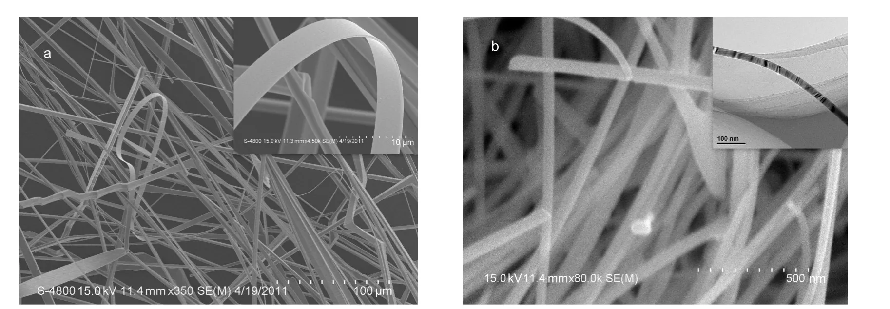
Fig.1 SEM images of the 1D structural SnO2belts prepared by the pure Sn particles(a)and theAu-modified Sn particles(b) Inserts show the corresponding high-magnification SEM image(a)and TEM image(b).
The water-assisted CVD has been employed to prepare well-crystalline SnO2nanowires,where Sn grains in large size were used as source materials.22Due to the large size of grains, the formed SnO2on the surface of grain will block the further transform of inner grain,thus leading to a lower yield of belts. We modified this method by replacing the big grains with small Sn particles or Au-modified small size Sn particles as source materials to successfully grow SnO2nanobelts in a transform yield of almost 100%.The Au-modified Sn powder was prepared by treating Sn powder in HAuCl4solution,and then exposing the mixture to UV light under vigorous stirring to reduce Au3+to Au on the Sn particle surface.Fig.1 shows the general morphologies of the prepared 1D structural SnO2with homogenous size in width and thickness.The geometrical shape of the two products observed by SEM is 1D well-defined belt structure.As the pure Sn particles were used as source materials,the belts can be prepared at 1050°C,and they are very long in the length direction about several millimeters,the width about 4-10 μm,and the thickness about 0.4 μm.Hereafter they are named as W-belts.But in the case of Au-modified Sn particles as the source materials,at 850°C,the belts can be grown in high yield,and the width of the prepared nanobelts shown in Fig.1b ranges from 40 to 70 nm.Hereafter they are named as N-belts.The detail growing mechanism due to the different source materials are discussed else.
XRD patterns of the 1D structural SnO2N-belts are shown in Fig.2a.All the diffraction peaks can be perfectly indexed to the tetragonal SnO2rutile phase structure.Moreover,no other impurity phase was detected and the neatly peaks revealed that the structures are well-crystallized.Fig.2b is the selected area electron diffraction(SAED)pattern.The SAED pattern taken along[1ˉ11]zone axis shows that the axial growth plane is(01ˉ1). Both the XRD and SAED indicate that the N-belt is single crys-talline,structurally uniform and dislocation-free.
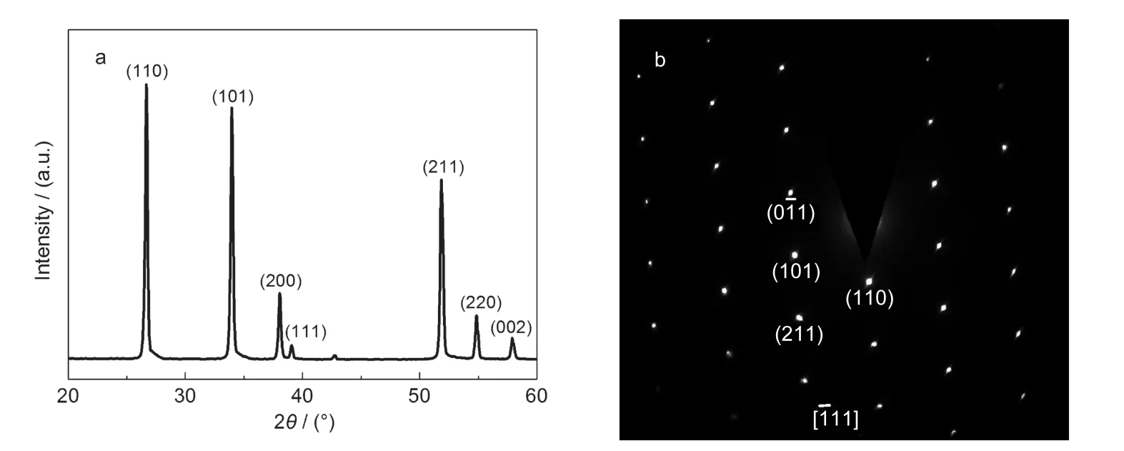
Fig.2 XRD(a)and SAED(b)patterns of SnO2N-belts
1D structure nanomaterials have been certificated to have improved charge transport properties,and 1D TiO2nanostructures,such as nanotube,nanowire,and nanorod,have been used in DSSCs for improving the light-to-electricity conversion efficiency.16,17,23However,nanobelts were seldom used in DSSCs,especially SnO2nanobelts have not yet used as photoelectrode materials to the best of our knowledge.Therefore, the prepared N-belts were mixed with commercial SnO2nanoparticles according to the different percentages from 20% to 100%(w)to prepare the composite thin film for fabrication of DSSCs.Table 1 summarizes the photovoltaic performance parameters of DSSCs based on the composite nanocrystalline thin films containing various amounts of SnO2N-belts.The photocurrent density and conversion efficiency vary with the mixing ratio of N-belts.The DSSC with addition of 20%(w) N-belts shows the best photovoltaic performance(short circuit photocurrent density(Jsc):4.72 mA·cm-2,open circuit photovoltage(Voc):371 mV,fill factor(FF):0.56,and conversion efficiency(η):0.98%)among all tested DSSCs in this study.N3 dye and iodide contained electrolyte used for dye sensitized TiO2nanocrystalline thin film solar cell are not suitable for SnO2nanocrystalline electrode in band structure,and we did nothing to optimize dye and electrolyte for the SnO2system, therefore,the DSSCs based on the composite SnO2thin films do not perform very good.But addition of N-belts at an optimum percentage of 20%(w)can obviously improve Jscabout 53%from 3.09 to 4.72 mA·cm-2.Over-addition of N-belts leads to a lower photocurrent due to the lower surface area of nanobelts compared to the nanoparticles.As 20%(w)W-belts were mixed in the SnO2nanocrystalline thin film,the Jscwas also increased compared with that of the pure nanocrystalline thin film without belts,but lower than the value of the one containing 20%(w)N-belts as shown in Fig.3.The lower photocurrent for W-belts is mainly due to its lower dye loading amount.
In order to analyze the dependent reason of the photocurrent on the addition of belts at different amounts and widths,we measured IMPS of the nanocrystalline thin film and the composite thin films containing 20%(w)N-belts or W-belts to further investigate the electron transport properties for the different nanocrystalline thin films.The IMPS measurement detects a combined response from the photoelectrode,the counter electrode,and the electrolyte.These processes at differentrates can be differentiated,because IMPS records the responses under the different frequencies.Fig.4 shows the IMPS spectra for the nanocrystalline thin films without and with 20%(w)N-belts or W-belts.The typical IMPS plot displays a semicircle in the complex plane.The transport time(τd)of electron in nanocrystalline thin film can be estimated from the equation of τd=(2πfmax)-1,where fmaxis the maximum characteristic frequency of the IMPS at the imaginary coordinate.24The value of τdgives an estimate of the average time that photoelectrons transport to the back contact,which determines the photocurrent of DSSCs.And the dye loading amount also influences the photocurrent,so we summarize the data of τdand dye loading amount in Table 2.
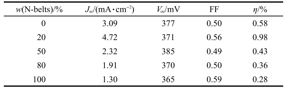
Table 1 Photovoltaic performance parameters of DSSCs based on the composite thin film electrode with different mixing amounts of N-belts
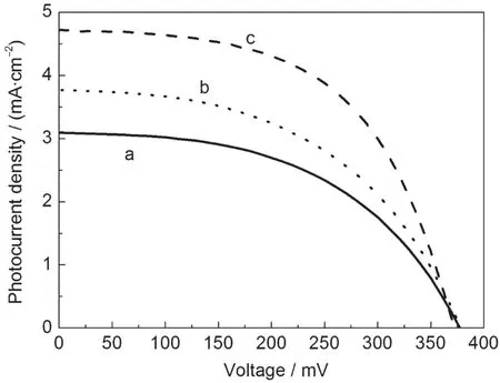
Fig.3 Photocurrent density-voltage characteristics of DSSCs (a)without 1D structural SnO2,(b)20%(w)W-belts,(c)20%(w)N-belts
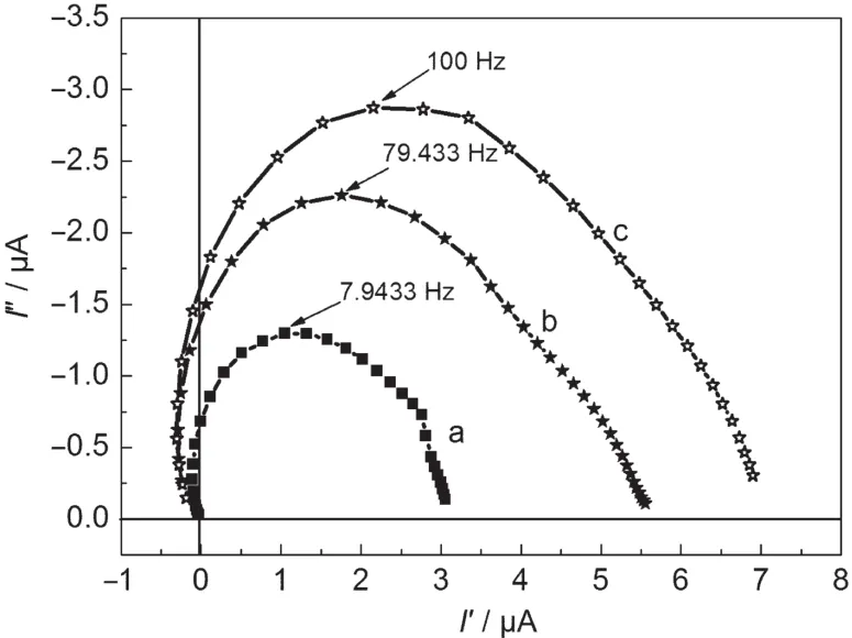
Fig.4 Intensity modulated photocurrent spectroscopies of DSSCs(a)without 1D structural SnO2,(b)20%(w)W-belts,(c)20%(w)N-belts

Table 2 Electron transport properties and dye loading amount of the composited photoelectrodes containing 20%(w)belts
In the case of addition of 20%(w)N-belts,the dye loading amount in the composite thin film is almost the same as that in the nanocrystalline thin film.But the electron transport time in two thin films is obviously different.With the addition of the 1D structural SnO2N-belts,the electron transport time decreases from 20.1 to 1.6 ms.The scattering reflection due to 1D belts in the nanocrystalline thin film can also contribute to the photocurrent of DSSC based on the composite thin film.We measured the scattering reflection spectra of the composite film with 20%(w)N-belts and the thin film without N-belts and estimated that photocurrent enhancement of about 10%for the composite thin film with 20%(w)N-belts is due to the scattering reflection of belts,and photocurrent enhancement of 43%is attributed to the good electron transport properties of 1D belt.In the case of the wide belts,the dye loading amount in the composite thin film with 20%(w)W-belts decreases due to the lower surface area of W-belts compared to N-belts, which makes photocurrent decrease.But it is still larger than that for the nanocrystalline thin film without any belt addition. The increasing in width of belt can not increase τdfurther.It is clear that the photocurrent does not only depend on the dye loading amount.Taking into consideration of the electron transporting time,scattering reflection,and dye loading amount,we can conclude that the higher electron transport ability of 1D structure is the main reason of the photocurrent enhancement by the addition of 1D structural SnO2.It is considered that the good crystallinity and the 1D geometry could allow the structure to support radial electric fields that could keep the electrons away from the surface,thereby reducing surface electron densities and recombination.25-28The 1D structural belt is an ideal candidate to act as an electron path for the rapid electron transport and thus leading to a good photovoltaic performance.
4 Conclusions
The well-crystallized 1D structural SnO2belts with different widths have been prepared using a simple water-assisted CVD method.DSSCs based on the composite SnO2nanocrystalline thin films with the well-crystallized 1D structural SnO2belts at different widths and added amounts were fabricated.DSSCs with 20%(w)SnO2N-belts showed the best photovoltaic performance.The 1D structural SnO2belt has high electron transport ability,and the addition of belts in a suitable amount can improve the photovoltaic performance.Therefore,well-crystallized 1D structural belt could be used in the composite nanocrystalline thin film to accelerate electron transport and thus improving the performance of DSSCs.
(1) OʹRegan,B.;Grätzel,M.Nature 1991,353,737.doi:10.1038/ 353737a0
(2) Grätzel,M.J.Photochem.Photobiol.2004,164,3.doi:10.1016/ j.jphotochem.2004.02.023
(3) Nazeeruddin,M.K.;Péchy,P.;Renouard,T.;Zakeeruddin,S. M.,Humphry-Baker,R.;Comte,P.;Liska,P.;Cevey,L.;Costa, E.;Shklover,V.;Spiccia,L.;Deacon,G.B.;Bignozzi,C.A.; Grätzel,M.J.Am.Chem.Soc.2001,123,1613.doi:10.1021/ ja003299u
(4) Pagliaro,M.;Palmisano,G.;Ciriminna,R.;Loddo,V.Energy Environ.Sci.2009,2,838.doi:10.1039/b903030a
(5) Berger,T.;Lana-Villarreal,T.;Monllor-Satoca,D.;Gómez,R. J.Phys.Chem.C 2007,111,9936.doi:10.1021/jp071438p
(6) Chen,D.H.;Huang,F.Z.;Cheng,Y.B.;Caruso,R.A.Adv. Mater.2009,21,2206.doi:10.1002/adma.200802603
(7) Qian,J.F.;Liu,P.;Xiao,Y.;Jiang,Y.;Cao,Y.L.;Ai,X.P.; Yang,H.X.Adv.Mater.2009,21,3633.
(8) Bierman,M.J.;Jin,S.Energy Environ.Sci.2009,2,1050.doi: 10.1039/b912095e
(9) Xiao,Y.M.;Wu,J.H.;Yue,G.T.;Lin,J.M.;Huang,M.L.;Fan, L.Q.;Lan,Z.Acta Phys.-Chim.Sin.2012,28,578. [肖尧明,吴季怀,岳根田,林建明,黄妙良,范乐庆,兰 章.物理化学学报,2012,28,578.]doi:10.3866/PKU.WHXB201201032
(10) Wang,Z.L.Adv.Mater.2000,12,1295.doi:10.1002/1521-4095 (200009)12:17<1295::AID-ADMA1295>3.0.CO;2-B
(11) Hu,J.T.;Odom,T.W.;Lieber,C.M.Accounts Chem.Res.1999, 32,435.doi:10.1021/ar9700365
(12) Xia,Y.N.;Yang,P.D.;Sun,Y.G.;Wu,Y.Y.;Mayers,B.;Gates, B.;Yin,Y.D.;Kim,F.;Yan,Y.Q.Adv.Mater.2003,15,353. doi:10.1002/adma.200390087
(13) Kang,S.H.;Choi,S.H.;Kang,M.S.;Kim,J.Y.;Kim,H.S.; Hyeon,T.;Sung,Y.E.Adv.Mater.2008,20,54.doi:10.1002/ adma.200701819
(14) Mor,G.K.;Shankar,K.;Paulose,M.;Varghese,O.K.;Grimes, C.A.Nano Lett.2006,6,215.doi:10.1021/nl052099j
(15) Feng,X.J.;Shankar,K.;Varghese,O.K.;Paulose,M.; Latempa,T.J.;Grimes,C.A.Nano Lett.2008,8,3781.doi: 10.1021/nl802096a
(16) Zhu,K.;Neale,N.R.;Miedaner,A.;Frank,A.J.Nano Lett. 2007,7,69.doi:10.1021/nl062000o
(17) Suzuki,Y.;Ngamsinlapasathian,S.;Yoshida,R.;Yoshikawa,S. Central Eur.J.Chem.2006,4,476.doi:10.2478/s11532-006-0015-3
(18) Asagoe,K.;Suzuki,Y.;Ngamsinlapasathian,S.;Yoshikawa,S. J.Phys.:Conf.Ser.2007,61,1112.doi:10.1088/1742-6596/61/ 1/220
(19) Prins,M.W.J.;Grosse-Holz,K.O.;Cillessen,J.F.M.;Feiner, L.F.J.Appl.Phys.1998,83,888.doi:10.1063/1.366773
(20) Dinh,N.N.;Bernard,M.C.;Goff,A.H.L.;Stergiopoulos,T.; Falaras,P.Comptes Rendus Chimie 2006,9,676.doi:10.1016/ j.crci.2005.02.042
(21) Xia,J.B.;Li,F.Y.;Yang,S.M.;Huang,C.H.Chin.Chem.Lett. 2004,5,619.
(22)Yin,W.Y.;Wei,B.Q.;Hu,C.W.Chem.Phys.Lett.2009,471, 11.doi:10.1016/j.cplett.2009.02.021
(23) Liu,R.H.;Zhang,S.;Xia,X.Y.;Yun,D.Q.;Bian,Z.Q.;Zhao, Y.L.Acta Phys.-Chim.Sin.2011,27,1701.[刘润花,张 森,夏新元,云大钦,卞祖强,赵永亮.物理化学学报,2011,27, 1701.]doi:10.3866/PKU.WHXB20110734
(24) Dloczik,L.;Ileperuma,O.;Lauermann,I.;Peter,L.M.; Ponomarev,E.A.;Redmond,G.;Shaw,N.J.;Uhlendorf,I. J.Phys.Chem.B 1997,101,10281.doi:10.1021/jp972466i
(25) Qu,J.;Gao,X.P.;Li,G.R.;Jiang,Q.W.;Yan,T.Y.J.Phys. Chem.C 2009,113,3359.doi:10.1021/jp810692t
(26) Pan,K.;Dong,Y.Z.;Tian,C.G.;Zhou,W.;Tian,G.H.;Zhao, B.F.;Fu,H.G.Electrochim.Acta 2009,54,7350.doi:10.1016/ j.electacta.2009.07.065
(27) Gonzalez-Valls,I.;Lira-Cantu,M.Energy Environ.Sci.2009,2, 19.doi:10.1039/b811536b
(28)Yang,Z.Z.;Xu,T.;Ito,Y.S.;Welp,U.;Kwoko,W.K.J.Phys. Chem.C 2009,113,20521.doi:10.1021/jp908678x
March 2,2012;Revised:May 8,2012;Published on Web:May 8,2012.
Electron Transport Properties of One-Dimensional Structural SnO2Belts
LI Xiao-Ning1,2BAI Shou-Li1,*YANG Wen-Sheng1CHENAi-Fan1SUN Li-Na1LIN Yuan2ZHANG Jing-Bo2,3,*
(1State Key Laboratory of Chemical Resource Engineering,Beijing University of Chemical Technology,Beijing 100029,P.R.China;2Beijing National Laboratory for Molecular Sciences,Institute of Chemistry,Chinese Academy of Sciences,Beijing 100190,P.R. China;3Tianjin Key Laboratory of Structure and Performance for Functional Molecules,
Tianjin Normal University,Tianjin 300387,P.R.China)
Well-crystallized one-dimensional(1D)structural SnO2belts are synthesized using a simple water-assisted chemical vapor deposition method.To increase the yield of SnO2belts,small Sn particles with and without Au-modifications are used as source materials to grow different width SnO2belts. Dye-sensitized solar cells(DSSCs)fabricated using the composite(nanoparticle/nanobelt)SnO2thin films, are used to evaluate the electron transport properties of the SnO2belts.Pastes containing different ratios of nanoparticles and belts are used to prepare the composite film by the doctor-blade method.The DSSCs exhibit different photovoltaic performances which are dependent on the nanoparticle/nanobelt ratio and width of the SnO2belts in the thin film.The enhanced electron transport properties of the composite films containing the SnO2belts is evaluated using intensity modulated photocurrent spectroscopy(IMPS).1D SnO2belts with a particular belt width improve the photovoltaic performance by providing electron paths to accelerate electron transport in the composite nanocrystalline thin films.
One-dimensional structural SnO2belt;Electron transport;Composite nanocrystalline thin film;Dye-sensitized solar cell;Photovoltaic performance
10.3866/PKU.WHXB201205081
O646
∗Corresponding authors.ZHANG Jing-Bo,Email:jbzhang@iccas.ac.cn;Tel:+86-10-82615031.BAI Shou-Li,Email:baisl@mail.buct.edu.cn;
Tel:+86-10-64434899.
The project was supported by the National Natural Science Foundation of China(20873162,51102011)and Natural Science Foundation of Beijing, China(8102028,8112022).
国家自然科学基金(20873162,51102011)和北京自然科学基金(8102028,8112022)资助项目
猜你喜欢
今日农业(2022年14期)2022-09-15
军事文摘(2022年14期)2022-08-26
科学大众(2021年21期)2022-01-18
小学科学(学生版)(2021年12期)2021-12-31
中国食用菌(2021年10期)2021-11-04
中南民族大学学报(自然科学版)(2018年4期)2018-12-29
北京航空航天大学学报(2017年2期)2017-11-24
中国塑料(2015年3期)2015-11-27
中国塑料(2015年9期)2015-10-14
中国塑料(2015年5期)2015-10-14
- 物理化学学报的其它文章
- 聚乙二醇对TiO2薄膜光致亲水性的促进作用
- MnO2的晶相结构和表面性质对低温NH3-SCR反应的影响
- Li修饰B12N12储氢行为的密度泛函理论研究
- 室温磷光材料二(2-苯基吡啶)(2-(2-吡啶)苯并咪唑)合铱(III)的合成及光电特性
- Coexistence of Oligonucleotide/Single-Chained Cationic Surfactant Vesicles with Precipitates
- Fluorescence Behavior of Biphenyl Containing Side-Chain Liquid Crystalline Polyacetylene with Various Lengths of Spacers