
铝热反应法制备双股类螺旋Zn2SnO4单晶纳米带
2012-12-11 09:35厉建龙张建平
物理化学学报 2012年10期
王 煜 陈 静 廖 清 孙 伟 厉建龙,* 张建平 吴 凯,*
(1北京大学化学与分子工程学院,北京分子科学国家实验室,北京100871;2中国科学院化学研究所,北京100190; 3中国人民大学化学系,北京100872)
铝热反应法制备双股类螺旋Zn2SnO4单晶纳米带
王 煜1陈 静1廖 清2孙 伟1厉建龙1,*张建平3吴 凯1,*
(1北京大学化学与分子工程学院,北京分子科学国家实验室,北京100871;2中国科学院化学研究所,北京100190;3中国人民大学化学系,北京100872)
综合利用化学气相沉积、铝热反应法、汽-液-固生长法、极性面融合和稳态湍流动力学控制来大量制备双股类螺旋Zn2SnO4单晶纳米带.该材料属于面心立方尖晶石型透明半导体,在光伏器件和湿度与可燃气体传感器中有着广泛的应用.扫描电镜、透射电镜、电子衍射、X射线衍射、拉曼光谱以及光发射等技术分析表明所得的双股类螺旋纳米带是由两个独立的Zn2SnO4纳米带通过扭曲纠缠和融合而成.该双股类螺旋纳米带实际上是在轴向具有周期性的超晶格材料.光致发光测量表明该纳米带在326.1 nm处出现强发射峰,线宽约为1.5 nm.本研究所采用的综合制备法中的铝热反应法和稳态湍流微扰法可能有助于类似材料的控制制备.
双股类螺旋纳米带;Zn2SnO4;铝热反应法;光致发光
1 Introduction
Controlling morphology and structure of nanomaterials plays a central role in tuning their properties for various applications.1-4Various types of one-dimensional(1D)inorganic nanomaterials5-14with different morphologies and structures have been fabricated in the past decade by using strategies like energy minimization,12lattice match-up,13and dislocation.14Nature is absolutely the master for designing and forming unique structures.One of its great masterpieces is the creation of bifilar or double-stranded helix DNA.People have been imitating natureʹs trick to synthesize helix-like materials due to their unique structures that possess chirality.In nanofabrication, many studies are related to unifilar or singe-stranded zigzag and helix-like inorganic nanowires and nanobelts,5-14and few works have focused on bifilar helix-like nanostructures.Developing a facile and efficient approach to synthesizing the bifilar helix-like nanostructures in a controlled manner is apparently a tough challenge.
Meanwhile,controlling the composition of the prepared inorganic nanomaterials is another big task in materials science.15-20Chemical reactions between oxides with cations of double and triple valence states frequently yield spinel and/or garnet composite oxides.When doped with some functional materials including rare earth elements and some transition metal ingredients,these composite oxides can be very useful in optics,electromagnetics,piezoelectrics and sensor.4In this research field, we have developed the interfacial reaction growth(IRG)approach21to growing integrated face-centered cubic(FCC)crystalline ZnAl2O4nanotube/nanonet22on porous alumina template and later on,crystalline ZnO(zinc spinel)nanonet on the grown ZnAl2O4nanonet by epitaxial growth.23,24Zn2SnO4(ZTO, zinc stanate),belonged to the FCC spinel,is an important transparent semiconductor with a band gap of 3.6 eV.25,26With high electron mobility,high electric conductivity,and low absorptivity of visible light,it is very useful in photovoltaic devices and sensors for humidity and various combustible gases.27-32Sparsely zigzagged Zn2SnO4nanowires were previously reported by employing thermal evaporation of ZnO/Sn powders under argon or nitrogen gas.33
Here we report the preparation in large quantity of 1D bifilar helix-like ZTO nanobelt(BHZN)consisting of two twisted zigzag nanobelts that merged together to form a single crystal. Each nanobelt was 50-70 nm wide and 20-30 nm thick and alternately grew along theanddirections.The chiral single crystal BHZN extended along the axial directionIts fabrication was realized by a strategy combining aluminothermal reaction approach,34vapor-liquid-solid (VLS) growth,polar-plane mergence,and steady-state turbulent gas flow control.Photoluminescence(PL)measurements showed that it had a strong light emission feature centered at about 326 nm with a line width of about 1.5 nm.
2 Experimental
2.1 Sample preparation and structural characterization
The applied aluminothermal reaction approach has been described in detail in a recent report.34In brief,mixed powder of ZnO,SnO2,and Al in a molar ratio of 1:2:12-1:4:12 was put in the front of an alumina boat,and a piece of Si wafer(4 mm×8 mm)coated with a thin gold layer of 20-40 nm in thickness was placed behind the mixed powder by a separation of 0.3-0.5 cm in the boat.The boat was then put into the constant temperature segment of a chemical vapor deposition(CVD) furnace.After purged by 100 cm3·min-1(standard state)high purity(>99.99%)N2flow(that flowed downstream from the mixed powder to the Si wafer)for 20 min,the boat was heated from room temperature(RT)to 950°C in 50 min in 30 cm3· min-1N2flow that was afterwards switched to two gas flows of 80 cm3·min-1N2and 20 cm3·min-1Ar through a 3-way gas valve.The boat was kept at 950°C for 30 min and then cooled in 30 cm3·min-1N2down to RT.The Si wafer was finally coated with a thin white layer of products that were directly used for morphology observations by scanning electron microscopy (SEM,Strata DB235,FEI and S4800,Hitachi)and environmental SEM(ESEM,Quanta 200F,FEI).The Si wafer was ultrasonicated in alcohol for 3 min and the suspension was dropped onto a copper grid for structural analyses by high-resolution transmission electron microscopy(HRTEM,Tecnai F30, Philips,300 kV).
2.2 Photoluminescence and Raman measurements
The samples used in the PL measurement were the as-prepared Zn2SnO4/Si wafer that was also mixed with a small amount of ZnO nanobelts and nanosaws.The as-prepared sample was optically pumped by the fourth harmonics of a Nd: YAG laser(266 nm in wavelength,4 Hz in frequency,5 ns in pulse time)at an incident angle of 45°.The light emission was collected along the sample surface normal direction with a polychromator(Spectropro 550i,Acton)equipped with a charge-coupled device(CCD)detector(SPEC-10-400B/LN, Roper Scientific)cooled with liquid nitrogen.Raman spectroscopy was also carried out on the same sample used for PL experiment.In Raman,an Ar+laser(488 nm in wavelength)was used as the excitation source and light reflected from the sample surface was collected by the CCD.
3 Results and discussion
The final products widely spread on a Si wafer that was about 3-4 mm away from the mixed precursor pile consisting of ZnO,SnO2and Al(for details of the products collection,refer to Fig.S1(a)in Supporting Information).Under our experimental conditions,the main part of the product on the Si wafer was Zn2SnO4and the left part was ZnO.This was verified by X-ray diffraction(XRD)measurements(Fig.S2(b)in Supporting Information).Normally these two kinds of products, Zn2SnO4and ZnO,mainly stayed in different collection zones, but the Zn2SnO4product could be also mixed with a small amount of ZnO.
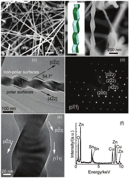
Fig.1 Large-scale(a)and magnified(b)ESEM images ofthe as-prepared BHZN on Si wafer.(c)TEM image(top view), (d)SAED pattern(with the e-beam perpendicular to the wire)and (e)enlarged TEM image(top view)of a BHZN.(f)EDX analysis of the BHZN in(e)The inset in(b)is the proposed side-view 3D model.Arrows in(c)and (e)mark the growth directions.The Cu signal in(f)was from the Cu grid used for the sample preparation.
The SEM image in Fig.1(a)demonstrates that 1D spindle-like nanowires with a periodicity along their axes were successfully synthesized.A closer look at a particular spindle-like nanowire(Fig.1(b))showed that it had a regular shape and was helix-like.Inset in Fig.1(b)is a possible 3-dimensional(3D) model for this helix-like nanowire(side view).TEM measurements(Figs.1(c)and 1(e))suggested the spindle-like nanowire actually contained two twisted zigzag nanobelts whose contacting parts merged together.The segments pointing lower right were longer than those pointing upper left(Fig.1(c),top view), implying that the growth directions of the two different segments might be with different lattice orientations(see Fig.2 and Supporting Information).Selected-area electron diffraction (SAED,Fig.1(d))with the e-beam perpendicular to the wire displayed a sharp pattern,indicating that it was a single crystal. By indexing the SAED pattern,the growth direction and individual crystal planes of the produced zigzag nanobelt could be deduced.Energy-dispersive X-ray(EDX)analysis in Fig.1(f) showed that it was made of three elements,Zn,Sn,and O,with a stoichiometric ratio of about 2:1:4.No Al signal was detected within the EDX measurement limit(about 5%).All of these measurements pointed out that the helix-like nanobelts were an FCC Zn2SnO4crystal,growing alternately along the[022],anddirections.The merged BHZN was~100 nm in diameter.
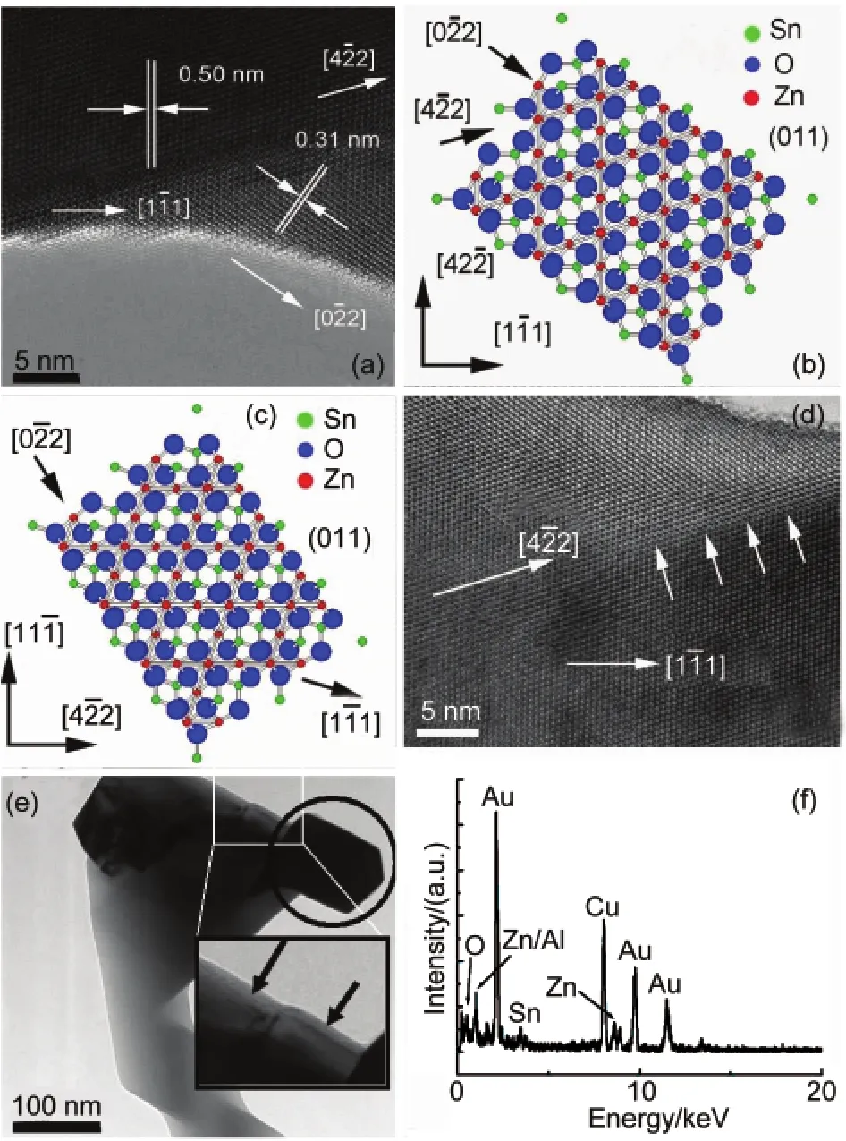
Fig.2 (a)HRTEM image of the lattice structure at the contacting part of the two ZTO nanobelts.(b)and(c)Atomic crystal models explaining the lattice structure shown in(a). (d)HRTEM image of another contacting section,showing the lattice dislocation indicated by the arrows.(e)TEM images of the endings of the BHZNs.(f)EDX analysis of the circled particle in(e)In(e),the rectangular cross-section(see the enlarged picture in the inset)of the ZTO nanobelt withAu particles attached can be clearly seen.Shorter arrow points the rectangular cross-sectional end of a ZTO nanobelt in the BHZN and the longer one indicates the ZTO nanobelt whose end actually curled.
To understand its structural details,HRTEM was used to image the lattice structures of a particular nanobelt along the nanobelt axis at different spots.The results(see Supporting Information)indicated that both nanobelts were single crystal. The lattice constant of the nanobelt along its own axis was about 0.50 nm(Fig.2(a)),corresponding to the inter-plane distance of theplanes.The lattice constant of the other along thedirection was 0.31 nm(Fig.2(a)),the inter-plane distance of theplanes.In consideration of the SAED patterns and the HRTEM fast Fourier transform(FFT) patterns(see Supporting Information),the growth direction of either nanobelt was deduced to be along
The existence of lattice dislocation(Fig.2(d))substantiated that the BHZN was indeed formed by two independent nano-belts.The possible formation mechanism of the BHZN was further studied with HRTEM.Figs.2(a)and 2(d)show the lattice structures and orientations around the merging section and the possible atomic structure models are given in Figs.2(b)and 2(c),respectively.Tentative analyses indicated that the BHZN grew along thedirection.The Zn,Sn,and O atoms in the side plane ofare symmetrically distributed,meaning that this plane is a non-polar one.However,when the same ZTO nanobelt changed its growth direction toits side direction waswhose corresponding face was theplane in which the Zn,Sn,and O atoms were asymmetrically distributed(Fig.2(c))and hence the side plane was polar(Fig.1(c)). Polar plane is not stable and tends to facet into non-polar planes in order to reduce the energy.This happened around the merging places of the two ZTO nanobelts.Although one of the polar side planes of each ZTO nanobelt still remained after merging,the BHZN energy was already substantially released during the merging process.Similar mechanism was previously reported for the merging of ZnO polar planes into a nanoring by Wang et al.35Fig.2(e)showed the situation where the twisting of the two ZTO nanobelts terminated or interrupted.In Fig.2(e),one could clearly see the rectangular cross section (pointed out by the shorter arrow in the inset in Fig.2(e))of the nanobelt end(Fig.2(e)).Itʹs from this rectangular cross-section that the thickness of a single ZTO nanobelt in BHZN was estimated to be around 20-30 nm.The width of the ZTO nanobelt was 50-70 nm(Fig.3(c)given below).In Fig.2(e),the belt width at the end was substantially larger than those in other parts,due to that the two nanobelts merged into one side by side[thefaces merged together]and their twisting ended. EDX measurement(Fig.2(f))of the circled particle on top of the BHZN in Fig.2(e)indicated that its main chemical composition was Au,implying that the ZTO nanobelt was grown through the VLS mechanism.It should be mentioned thatand its equivalent planes are highly indexed planes with high surface energy.To reduce this high surface energy,the end planeof the ZTO nanobelt could facet,which we might not detect with TEM or SEM due to technical limitation.However,a highly indexed face may also be stabilized by adsorbing foreign atoms/molecules or by coating with a layer of foreign film that has small surface energy.We feel that the latter may happen in our case because,as indicated by Figs.2(e)and 2(f), the end of the ZTO nanobelt was attached with a fairly large Au particle.
Figs.3(a)and 3(b)are the SEM and TEM images of isolated single ZTO nanobelts.In Fig.3(b),the electron diffraction pattern(with the e-beam perpendicular to the ZTO nanobelt) shows the same diffraction pattern as that shown in Fig.1(d) for the BHZN(Fig.1(c)),meaning that the ZTO nanobelt has the same lattice structure and growth orientation as those in the BHZN.Moreover,we could observe by TEM a BHZN with a“normal”splitting end after its growth was interrupted.This is shown in Fig.3(c).One can see that the two ZTO nanobelts forming the BHZN split again,as indicated by the arrow in Fig.3(c).All these strongly support that the BHZN is composed of two ZTO nanobelts.
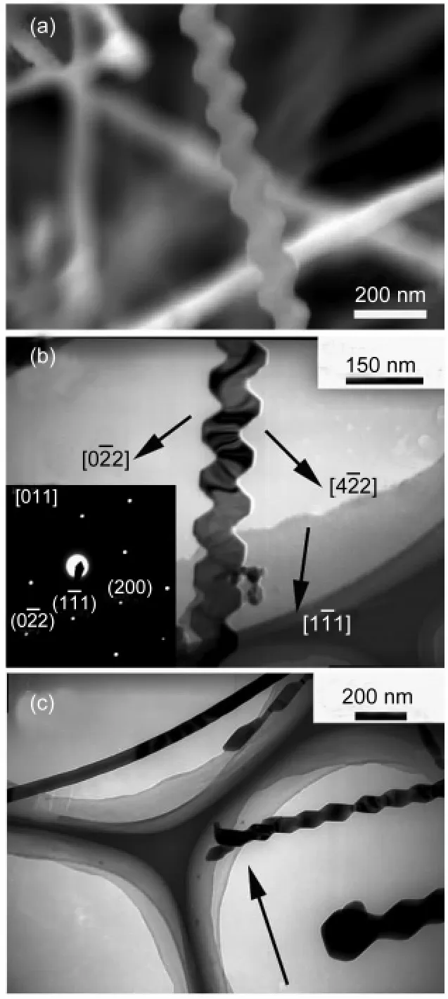
Fig.3 (a)SEM and(b)TEM images of isolated single zigzag ZTO nanobelts.The inset in(b)is the ED pattern of the ZTO nanobelt with the e-beam perpendicular to the zigzag ZTO nanobelt. (c)TEM image of a BHZN,showing that its end split into two ZTO nanobelts again after the growth was interrupted.
Since the possibility of forming either left-handed(Fig.4(b)) or right-handed(Fig.4(c))structure is equal and hence,we could find both of them in the as-prepared samples.Obviously, the BHZN structure in Fig.4(c)can only be obtained by a mirror operation of the structure in Fig.4(b).Figs.4(a)and 4(d)are the proposed top-view 3D models(projected perpendicular to the axial directionfor the BHZN structures in Figs.4(b) and 4(c),respectively.The BHZN structure is quite similar to that of DNA,except for that the two ZTO nanobelts were bound together by lattice merging rather than the hydrogen bonds between the base pairs in DNA.
The involved chemical reactions in the CVD device can be written as:
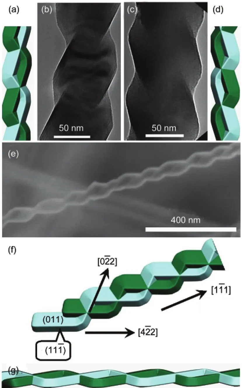
Fig.4 Two zigzag ZTO nanobelts twisted into one.The twisting could happen in two ways,ending up with either left-handed BHZN(b)or right-handed BHZN(c).(a)and(d)are the corresponding top-view 3D models for(b)and(c),respectively. (e)Perspective-view SEM image and(f)3D model of a tilted BHZN.(g)Side-view 3D model of the BHZN
Without Al,we did not obtain any BHZNs under our experimental conditions.Moreover,no Al signal was detected in the final products on the Si wafer,meaning that Al served as a reductant and its reaction with ZnO and SnO2to form Al2O3via reactions(1),(2),and(2ʹ)also released a large amount of local heat spurring following reactions.The oxygen came from the residual gas in CVD.In our experiments,Au layer on the Si wafer was employed.Without the Au layer,no Zn2SnO4products were detected,indicating that Au might serve as a catalyst for the Zn2SnO4formation via the so-called VLS mechanism. In Fig.2(e),Au particles clearly existed at the ends of both ZTO nanobelts,supporting the VLS mechanism proposal.
To verify the above deductions,we carried out a series of control experiments.Without the Au layer on Si wafer,no BHZNs were synthesized under our experimental conditions. On the other hand,under the same experimental conditions without the precursors,the Au layer on the Si wafer shrank into many small nanoparticles ranging from 60 to 80 nm in diameter(see Supporting Information),in good agreement with the Au size detected at the BHZN end shown in Fig.2(e).If we put the precursors in,raised the temperature to 950°C in 50 min in 30 cm3·min-1N2and then swiftly cooled the sample down to RT,observed were some short nanowires on top of which the Au particles were seated(Supporting Information).This further supports the VLS growth mechanism.Under the same experimental conditions as for Figs.1(a)and 1(b),single zigzag ZTO nanobelt was also identified(Fig.3).However,if 100 cm3· min-1N2was introduced into the CVD system instead of 80 cm3·min-1N2and 20 cm3·min-1Ar,no zigzag nanostructure or BHZN was synthesized,showing that the turbulent flow is a must for the appearance of the zigzag nanobelt and BHZN.
To understand the role of the turbulent flow gas,we added a gas reservoir(acting as a gas buffer)between the 3-way gas valve and the CVD device so that the gases were thoroughly pre-mixed before entering the CVD tube.With such a modification,no BHZN was detected,indicating that the two independent gas flows played an important role in tuning the morphology of the products.The two independent gas flows might form a wave-like turbulence in CVD that affects the structure orientation of BHZN separated out of the Zn,Sn,and Au alloy on the Si wafer.
To further verify the attribution of the chemical composition of the BHZN,Raman measurement was taken.Since the Si wafer substrate had a resonant feature at about 520 nm,the experimentally measured Raman spectroscopy was calibrated by subtracting the Si signal.The calibrated Raman spectroscopy is shown in Fig.5(a).Four sharp Raman features at about 666.4, 526.6,225.3,and 110.3 cm-1can be clearly identified.The 666.4 cm-1feature is the main one.According to the literature,26,32these four features can be assigned to the Raman resonances of Zn2SnO4.The sharpness of the measured Raman features in our experiment suggested that the BHZN was in good crystallinity.26Again,the Raman result evidenced that the chemical composition of the prepared BHZN was fcc spinel Zn2SnO4.
Putting all above experimental facts together,we can now work out a picture for the growth of the BHZN under our experimental conditions.Initially,ZnO and SnO2were reduced by Al to produce Zn and Sn vapor,meanwhile the Au layer on Si wafer shrank into small Au particles.At 950°C,the Zn and Sn vapor dissolved into liquid Au particles.After exceeding the saturation concentration,solid Zn and Sn crystallized out of the liquid and immediately reacted with residual oxygen to yield ZTO nanobelts via reactions(3)and(3ʹ).Under the disturbance of a steady-state turbulent gas flow of N2and Ar,the growth directions of the ZTO nanobelts would be perturbed to produce the zigzag structures(Figs.3(b)and 3(c)).With time going on at such a high temperature,these zigzagged ZTO nanobelts would twist(Fig.4)and finally merged at their contacting sections(Figs.2(a)and 2(d)).Fig.4(f)is a perspective-view 3D model for the produced BHZN in Fig.4(e).The two zigzag ZTO nanobelts grow along the[022],[111],and [422]directions,alternately.Their side planes including the polar(111)and non-polar(011)planes would merge together at high temperatures.To enhance visibility,we use two colors to discriminate each zigzag ZTO nanobelt in the BHZN in the 3D models.In reality,any contacting parts between the two zigzag ZTO nanobelts merge into an integrated one.Fig.4(g)displays a side-view 3D model for the BHZN,showing the up-anddown fluctuation of both ZTO nanobelts in the BHZN.This means that these ZTO nanobelts are actually in zigzag form projected along both the top-view(Fig.4(a)or Fig.4(d))and the side-view(Fig.4(g))directions.
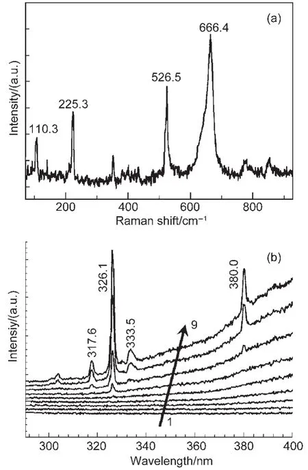
Fig.5 (a)Raman spectroscopy and(b)PLmeasurement of the as-prepared sampleIn(a),the Si background was deducted by using bare Si wafer as the blank experimental sample.The energy densities of the incident pump laser for traces 1 through 9 in(b)were 3.1,5.3,11,25,38,66,120,240, and 510 mJ·cm-2,respectively.
ZTO is a transparent semiconductor oxide,so its PL measurement should be interesting.This is shown in Fig.5(b).With the energy density increase of the pump laser,a feature at 326.1 nm first appeared and followed by the features at 333.5, 317.6,and 380.0 nm.Since in our experimental conditions,a small portion of ZnO nanobelts could also exist(supporting information),the 380.0 nm feature is much likely due to the presence of ZnO nanostructures and similar to the PL feature from ZnO nanonet reported in our previous study.23The reported band gap of Zn2SnO4 was about 3.6 eV,25,26corresponding to a light wavelength of about 344 nm.The main feature at 326.1 nm in PL can be attributed to the characteristic emission of Zn2SnO4.The blue shift of the main feature might be due to the quantum confinement effect.There could be other factors that may cause the blue shift of the main feature,but this needs further investigation.
Blue shift of the PL features for semiconductor materials has been frequently reported36-40as their sizes downsize from bulk to nanoscale.For example,the band gap of bulk GaN is about 3.40 eV,corresponding to 364.7 nm in wavelength.When the GaN material downsized to a nanostructure of 40 nm in thickness and 120 nm in diameter,its PL feature centered at about 3.472 eV(357.1 nm),with a shift of about 7.6 nm in wavelength.Further decrease of its size led to a PL feature at about 3.581 eV(346.3 nm),corresponding to a shift in wavelength as large as 18.4 nm.39Therefore,our observation of the blue shift for the BHZN by 18 nm from that for bulk Zn2SnO4is not unusual.In fact,Palmer and Poeppelmeier25had reported the diffuse reflectance(approximate transmission)spectra of Zn2SnO4whose starting edge was about 330-340 nm,also in agreement with our result.Therefore,the main feature at 326.1 nm is attributed to the light emission from the BHZN.Since the line width(FWHM,full width at half maximum)was quite narrow (about 1.5 nm)and there existed an energy density threshold for the pump laser,this emission was likely to be the stimulated emission rather than the spontaneous one.
At both sides of the main feature appeared new features at 333.5 and 317.6 nm were quite puzzling.Due to the strong intensity(as high as 7000 cps in experiment)and narrow line width(about 1.5 nm,its full width at half maximum)of the main feature,the main PL emission feature may act as a new excitation light.If this were true,then the main Raman resonance in Fig.5(a)could appeared as Stokes and anti-Stokes lines.Since the main Raman resonance wave number is 666.4 cm-1,corresponding to about 0.083 eV in energy,the wavelengths of the Stokes and anti-Stokes Raman lines around the 326.1 nm feature would be 333.4 and 319.1 nm,respectively. These calculated wavelength values are in good agreement with our measured ones in Fig.5(b).An alternative possible explanation of the two small features around the main one in PL could be distortion of the energy band caused by the lattice distortion and dislocation in the BHZN.The origin of the weak feature at about 303 nm is unclear at the moment.We did observe a big lump feature between 400-600 nm.This was ascribed to the vacancy or surface states or defects in the crystal.32
4 Conclusions
To conclude,we have successfully prepared bifilar helix-like single crystalline Zn2SnO4nanobelt(BHZN)by exploiting the aluminothermal reaction,VLS growth mode with Au,the merging of polar planes and kinetic control with steady-state turbulent gas flow.The BHZN was formed by the twisting of two ZTO nanobelts.Each ZTO nanobelt alternately grew along the [022],[111],and[422]directions.They finally merged into one nanobelt at 950°C whose axial direction was[111]and diameter was about 100 nm.The BHZN displayed a periodicity along the axial direction,forming an actual super-lattice structure whose side faces were still polar.The PL measurements showed a strong light emission at 326.1 nm from the BHZN sample with a line width of about 1.5 nm.The combined approach used in this study,in particular its aluminothermal reaction and steady-state turbulent gas flow perturbation steps,may be helpful in preparing other materials.The BHZN structure may have potential applications in piezoelectrics,optoelectrics, and gas sensors.
Supporting Information:available free of charge via the internet at http://www.whxb.pku.edu.cn.
(1)Wang,Z.L.Dekker Encyclopedia of Nanoscience and Nanotechnology 2004,1773.
(2) Chen,J.Y.;Benjamin,W.;Joseph,M.;Xiong,Y.J.;Li,Z.Y.; Xia,Y.N.Nano Lett.2005,5,2058.doi:10.1021/nl051652u
(3) Kuang,Q.;Jiang,Z.Y.;Xie,Z.X.;Lin,S.C.;Lin,Z.W.;Xie, S.Y.;Huang,R.B.;Zheng,L.S.J.Am.Chem.Soc.2005,127, 11777.doi:10.1021/ja052259t
(4) Benjamin,D.Y.;David,O.Z.;Peter,J.P.;He,R.R.;Yang,P.D. Angew.Chem.Int.Edit.2006,45,420.doi:10.1002/(ISSN) 1521-3773
(5) Zhang,H.F.;Wang,C.M.;Wang,L.S.Nano Lett.2002,2,941. doi:10.1021/nl025667t
(6)Zhang,D.Q.;Abdullah,A.;Han,H.G.;Hasan,M.;McIlroy,D. N.Nano Lett.2003,3,983.doi:10.1021/nl034288c
(7)Vardhan,B.;Dai,L.M.;Toshiyuki,O.J.Am.Chem.Soc.2004, 126,5070.doi:10.1021/ja031738u
(8) Zhang,G.Y.;Jiang,X.;Wang,E.G.Appl.Phys.Lett.2004,84, 2646.doi:10.1063/1.1695198
(9) Gao,R.P.;Wang,Z.L.;Fan,S.S.J.Phys.Chem.B 2000,104, 1227.doi:10.1021/jp9937611
(10)Tang,Y.H.;Zhang,Y.F.;Wang,N.;Lee,C.S.;Han,X.D.; Bello,I.;Lee,S.T.J.Appl.Phys.1999,85,7981.doi:10.1063/ 1.369389
(11) Duan,J.H.;Yang,S.G.;Liu,H.W.;Gong,J.F.;Huang,H.B.; Zhao,X.N.;Zhang,R.;Du,Y.W.J.Am.Chem.Soc.2005,127, 6180.doi:10.1021/ja042748d
(12) Yang,R.S.;Ding,Y.;Wang,Z.L.Nano Lett.2004,4,1309. doi:10.1021/nl049317d
(13) Bae,S.Y.;Lee,J.Y.;Jung,H.S.;Park,J.H.;Ahn,J.P.J.Am. Chem.Soc.2005,127,10802.doi:10.1021/ja0534102
(14) Zhan,J.H.;Bando,Y.;Hu,J.Q.;Xu,F.F.;Golberg,D.Small 2005,1,883.doi:10.1002/(ISSN)1613-6829
(15) Zarur,A.J.;Ying,J.Y.Nature 2000,403,65.doi:10.1038/ 47450
(16) Shen,S.C.;Kus,H.;Liya,E.Y.;Sibudjing,K.Adv.Mater. 2004,16,541.doi:10.1002/(ISSN)1521-4095
(17) Chen,Y.C.;Chang,Y.H.;Tsai,B.S.Mater.Trans.2004,45, 1684.doi:10.2320/matertrans.45.1684
(18)vander Laaga,N.J.;Snela,M.D.;Magusinb,P.C.M.M.;de With,G.J.Eur.Cer.Soc.2004,24,2417.doi:10.1016/ j.jeurceramsoc.2003.06.001
(19) Lou,Z.D.;Hao,J.H.Thin Solid Films 2004,450,334.doi: 10.1016/j.tsf.2003.11.294
(20) Zawadzki,M.;Wrzyszcz,J.;Strek,W.;Hreniak,D.J.Alloy. Compd.2001,323-324,279.
(21)Yu,J.F.;Wang,F.;Wang,Y.;Gao,H.;Li,J.L.;Wu,K.Chem. Soc.Rev.2010,39,1513.doi:10.1039/b812787p
(22)Wang,Y.;Wu,K.J.Am.Chem.Soc.2005,127,9686.doi: 10.1021/ja0505402
(23)Wang,Y.;Liao,Q.;Lei,H.;Zhang,X.P.;Ai,X.C.;Zhang,J.P.; Wu,K.Adv.Mater.2006,18,943.doi:10.1002/(ISSN) 1521-4095
(24)Liao,Q.;Wang,Y.;Li,J.L.;Wu,K.;Ai,X.C.;Zhang,J.P. Appl.Phys.Lett.2007,91,041103.doi:10.1063/1.2759473
(25) Palmer,G.B.;Poeppelmeier,K.R.Solid State Sci.2002,4,317. doi:10.1016/S1293-2558(01)01258-4
(26) Coutts,T.J.;Young,D.L.;Li,X.;Mulligan,W.P.;Wu,X. J.Vac.Sci.Technol.A 2000,18,2646.
(27) Stambolova,I.;Konstantinov,K.;Kovacheva,D.;Peshev,P.; Donchev,T.J.Solid State Chem.1997,128,305.doi:10.1006/ jssc.1996.7174
(28)Yamada,Y.;Seno,Y.;Masuoka,Y.;Yamashita,K.Sens.Actua. B-Chem.1998,49,248.doi:10.1016/S0925-4005(98)00135-X
(29) Stambolova,I.;Konstantinov,K.;Khristova,M.;Peshev,P. Phys.Status Solid.-Appl.Res.1998,167,R11.
(30) Jie,J.S.;Wang,G.Z.;Han,X.H.;Fang,J.P.;Yu,Q.X.;Liao, Y.;Xu,B.;Wang,Q.T.;Hou,J.G.J.Phys.Chem.B 2004,108, 8249.doi:10.1021/jp049230g
(31)Chen,H.Y.;Wang,J.X.;Yu,H.C.;Yang,H.X.;Xie,S.S.;Li, J.Q.J.Phys.Chem.B 2005,109,2573.doi:10.1021/jp046125y
(32)Wang,J.X.;Xie,S.S.;Gao,Y.;Yan,X.Q.;Liu,D.F.;Yuan,H. J.;Zhou,Z.P.;Song,L.;Liu,L.F.;Zhou,W.Y.;Wang,E.G. J.Cryst.Growth 2004,267,177.
(33)Kim,H.S.;Hwang,S.O.;Myung,Y.;Park,J.;Bae,S.Y.;Ahn, J.P.Nano Lett.2008,8,551.doi:10.1021/nl072829i
(34)Yu,J.F.;Wang,Y.;Wen,W.;Yang,D.H.;Huang,B.;Li,J.L.; Wu,K.Adv.Mater.2010,22,1479.doi:10.1002/adma. 200903656
(35) Kong,X.Y.;Ding,Y.;Yang,R.S.;Wang,Z.L.Science 2004, 303,1348.doi:10.1126/science.1092356
(36) Gates,B.;Mayers,B.;Cattle,B.;Xia,Y.N.Adv.Funct.Mater. 2002,12,219.doi:10.1002/1616-3028(200203)12:3<219:: AID-ADFM219>3.0.CO;2-U
(37) Joo,J.;Son,J.S.;Kwon,S.G.;Yu,J.H.;Hyeon,T.J.Am. Chem.Soc.2006,128,5632.doi:10.1021/ja0601686
(38) Goodwin,T.J.;Leppert,V.J.;Risbud,S.H.;Kennedy,I.M.; Lee,H.W.H.Appl.Phys.Lett.1997,70,3122.doi:10.1063/ 1.119109
(39) Ramyall,P.;Tanaka,S.;Nomura,S.;Riblet,P.;Aoyagi,Y.Appl. Phys.Lett.1998,73,1104.doi:10.1063/1.122098
(40) Hu,P.A.;Liu,Y.Q.;Fu,L.;Cao,L.C.;Zhu,D.B.J.Phys. Chem.B 2004,108,936.
August 28,2012;Revised:September 10,2012;Published on Web:September 11,2012.
Bifilar Helix-Like Nanobelt of Single Crystalline Zn2SnO4Fabricated by Aluminothermal Reaction Approach
WANG Yu1CHEN Jing1LIAO Qing2SUN Wei1LI Jian-Long1,*ZHANG Jian-Ping3WU Kai1,*
(1Beijing National Laboratory for Molecular Sciences,College of Chemistry and Molecular Engineering,Peking University, Beijing 100871,P.R.China;2Institute of Chemistry,Chinese Academy of Sciences,Beijing 100190,P.R.China;3Department of Chemistry,Remin Unversity of China,Beijing 100872,P.R.China)
This paper reports the preparation in large quantity of bifilar helix-like nanobelts of single crystalline Zn2SnO4,a face-centered cubic spinel and transparent semiconductor that possesses wide applications in photovoltaic devices and sensors for humidity and combustible gases,by using a unique approach that combines chemical vapor deposition,aluminothermal reaction,vapor-liquid-solid growth, mergence of polar planes,and kinetic control by steady-state turbulent flow.The bifilar helix-like nanobelt was formed by the twisting and merging of two independent Zn2SnO4nanobelts,as analyzed by scanning electron microscopy,transmission electron microscopy,electron diffraction,X-ray diffraction,Raman spectroscopy,and photoluminescence.It had a periodicity along the axial direction and hence,is actually a super-lattice material.The photoluminescence measurements showed a strong light emission at 326.1 nm from the as-prepared sample with a line width of about 1.5 nm.The combined approach used in this study, in particular its aluminothermal reaction and steady-state turbulent gas flow perturbation steps,may be helpful in preparing other similar materials.
Bifilar helix-like nanobelt;Zn2SnO4;Aluminothermal reaction approach; Photoluminescence
10.3866/PKU.WHXB201209113
∗Corresponding authors.WU Kai,Email:kaiwu@pku.edu.cn;Tel:+86-10-62754005.LI Jian-Long,Eamil:jlipku@pku.edu.cn; Tel:+86-10-62757062.
The project was supported by the National Natural Science Foundation of China(20827002,20911130229)and National Key Basic Research Program of China(973)(2009CB929403,2011CB808702).
国家自然科学基金(20827002,20911130229)及国家重点基础研究发展规划项目(973)(2009CB929403,2011CB808702)资助
O641
猜你喜欢
上海城市管理(2022年6期)2022-11-28
纺织科学研究(2020年4期)2020-04-30
山东工业技术(2019年8期)2019-05-29
速读·中旬(2017年10期)2017-10-23
中国高新技术企业(2017年5期)2017-05-05
中国科技信息(2016年19期)2016-10-25
中国科技信息(2016年6期)2016-08-31
浙江共产党员(2016年7期)2016-06-01
中国科技信息(2015年24期)2015-11-07
中国科技信息(2015年23期)2015-11-07
