基片温度对镓钛共掺杂氧化锌透明导电薄膜性能的影响
2013-11-26 05:45钟志有
中南民族大学学报(自然科学版) 2013年1期
钟志有,张 腾,汪 浩
(中南民族大学电子信息工程学院,武汉430074)
有机光伏电池具有轻薄、成本低、能卷曲、环境友好、容易实现大面积制造等独特优势[1-3],在便携式计算机、半透光式充电器以及柔性可卷曲系统等体系中具有潜在的应用前景,是未来最为廉价和最有吸引力的能源模式之一.自从1986年 Tang[4]发明电子给体-受体双层结构的有机光伏电池以来,人们从电池结构、器件机理、光伏材料和制备工艺等各个方面卓有成效地开展了研究,电池的性能获得了明显提高[5-7].众所周知,有机光伏电池的典型结构为三明治夹心结构,即依次由透明导电阳极、有机活性层和金属阴极组成,其中,电池阳极一般采用掺锡氧化铟(ITO)透明导电玻璃,但由于铟(In)、锡(Sn)自然储量较少、制备工艺复杂、成本高、有毒性、稳定性不理想等原因,从而将极大影响未来光伏电池的推广应用,因此,研制可以替代ITO产品的透明导电薄膜已经成为该领域的重要课题之一.
氧化锌(ZnO)是II-VI族n型半导体材料,在室温条件下直接光学能隙约为3.37 eV[8],它具有良好的导电性和透光性,在发光器件、光伏电池、液晶显示器、透明电磁屏蔽以及触敏覆盖层等众多领域得到了非常广泛的应用[9,10].与目前普遍使用的ITO相比,ZnO薄膜具有自然储量丰富、价格低廉、在活性氢和氢等离子体环境下稳定性高等优点而备受青睐.研究表明,Al、B、Ti、Zr、Ga 等单元素掺杂能够较大幅度地提高ZnO薄膜的导电能力,但其光学性能和化学稳定性却仍然不尽如人意.为此,近几年人们开始尝试采用 Al-Mn[11]、Ga-B[12]、Li-Mg[13]、Al-Sc[14]、Al-Zr[15]、Mn-Co[16]等共掺杂方法来获得具有优良光电性能的ZnO透明导电薄膜.对于共掺杂ZnO透明导电薄膜,其主要制备方法有脉冲激光沉积 法[17,18]、喷雾热分解法[19]、化学气相沉积法[20]、射频溅射法[21,22]、直流溅射法[23,24]、溶胶-凝胶法[25-27]等,其中磁控溅射技术具有设备简单、价格便宜、易于掺杂等特点,所制备的薄膜不仅均匀致密、表面平整、附着性好,而且c轴取向性好、可见光区透过率高,因此它是目前掺杂ZnO薄膜最常用的制备方法之一.本文以镓钛共掺杂氧化锌(GTZO)陶瓷靶作为靶材,采用射频磁控溅射技术制备了GTZO无铟透明导电薄膜,通过 X射线衍射仪(XRD)、分光光度计和四探针仪等测试表征,研究了基片温度对薄膜结晶质量、电学性质和光学性能的影响.
1 实验
1.1 基片处理
实验选用普通玻璃作为基片材料,首先采用丙酮擦拭玻璃基片表面,然后用清水冲洗干净,再依次使用丙酮、无水乙醇和去离子水各超声清洗约15 min,最后在无水乙醇中煮沸,吹干待用.
1.2 薄膜制备
利用射频磁控溅射技术在玻璃基片上制备透明导电的GTZO薄膜,所用实验设备为国产KDJ567型高真空复合镀膜系统,所用溅射靶材的直径为50 mm、厚度为4 mm,它由ZnO、Ga2O3和 TiO2混合烧结而成,ZnO、Ga2O3和TiO2的纯度均为99.99%,其中ZnO、Ga2O3和TiO2的质量分数分别为97%、1.5%和1.5%.溅射所用气体为纯度99.99%的高纯氩气,GTZO薄膜沉积之前,先将玻璃基片放置于镀膜系统的真空室中,待气压抽至低于5×10⁻⁴Pa后通入氩气,并先采用氩离子体对基片表面清洗约3 min,然后再对靶材表面预溅射5 min以去除其表面的杂质和污染物.实验时,制备GTZO薄膜的具体工艺参数如下:溅射功率为200 W,靶-基距离为70 mm,工作压强为0.5 Pa,氩气流量为15 sccm,溅射时间为40 min,基片温度分别为300℃、350℃和400℃.
1.3 性能表征
GTZO薄膜的晶体结构采用德国Bruker公司的D8-ADVANCE型X射线衍射仪(Cu Kα,射线源的波长λ=0.15406 nm)分析,薄膜的方块电阻利用SZ-82型数字式四探针仪测试,薄膜的光学性能使用TU-1901型双光束紫外-可见光分光光度计进行表征.
2 结果与讨论
2.1 薄膜的微观结构
不同基片温度时所制备GTZO薄膜样品的XRD图谱如图1所示,由图可见,所有GTZO样品的特征谱线与均ZnO薄膜六角纤锌矿结构的特征谱线相吻合,这说明GTZO薄膜样品均具有六角纤锌矿结构,并且存在(002)方向上的择优取向.另外从XRD图谱看出,对于所有GTZO薄膜,在衍射峰位34.4°附近存在一个很强的(002)衍射峰,并且没有检测到Ga2O3相和TiO2相的存在,这说明掺杂到薄膜当中的Ga原子和Ti原子均以替位形式取代了六角晶格中的部分Zn原子的位置,或者它们弥散在薄膜的晶粒间界区域[28,29],对于不同元素掺杂的 ZnO薄膜,也有类似结果的报道[30-32].
图2为GTZO薄膜(002)衍射峰位2θ及其衍射强度随基片温度的变化关系,可以看出,基片温度对GTZO样品(002)衍射峰位的影响并不明显,但对(002)峰的衍射强度具有较为显著的影响,当基片温度为300℃、350℃和400℃时,GTZO薄膜(002)峰衍射强度分别为3.5 ×10⁵cps,6.6 ×105cps,6.3×105cps,呈现出先升高、后降低的变化趋势,其中基片温度为350℃时所对应的衍射峰强度最大.
GTZO样品(002)衍射峰半高宽(B)随基片温度的变化如图3(a)所示,由图可知,基片温度升高时,半高宽B先逐渐减小、后逐渐增加,当基片温度为350℃时GTZO薄膜的B值最小,大约为0.162°.基于(002)衍射峰的峰位2θ值和对应的半高宽B,不同基片温度时GZTO薄膜的晶粒尺寸(D)可以根据 Debye-Scherrer公式[33,34]计算:

公式(1)中,θ为衍射角,λ为X射线的波长(对于铜靶,λ=0.15406 nm),k为形状因子(这里取 k=0.89)[35].不同基片温度时所制备 GTZO 样品的晶粒尺寸D如图3(b)所示,从图中可以看出,当基片温度为300℃,350℃和400℃时,GTZO样品的晶粒尺寸 D 分别为36.6 nm,50.8 nm 和45.9 nm,结果说明GTZO薄膜的晶粒尺寸D明显受到基片温度的影响,D随基片温度的变化趋势与半高宽B相反,当基片温度为350℃时样品的晶粒尺寸最大(50.8 nm).
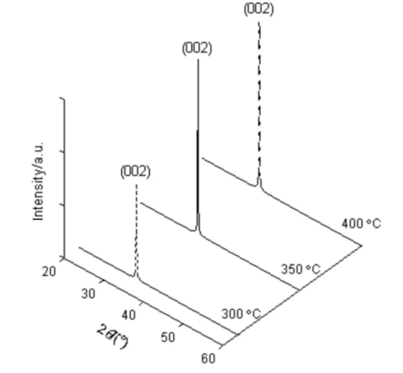
图1 不同基片温度时样品的XRD图谱Fig.1 XRD patterns of the samples deposited with different substrate temperatures
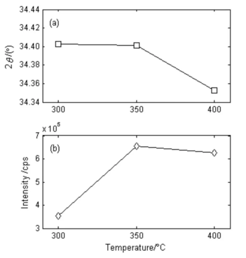
图2 不同基片温度时样品的(002)峰位置和衍射强度Fig.2 The peak position(2θ)(a)and intensity(b)of(002)plane for the samples deposited with different substrate temperatures
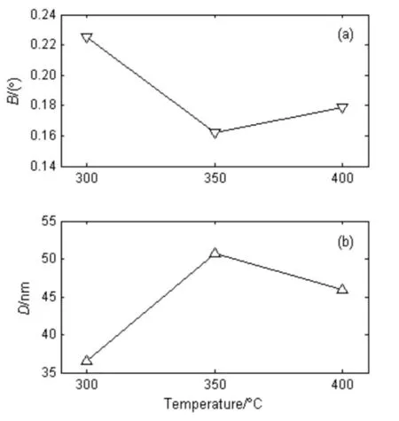
图3 不同基片温度时样品的(002)峰半高宽和晶粒尺寸Fig.3 The full-width at half-maximum(B)(a)and grain size(D)(b)of(002)plane for the samples deposited with different substrate temperatures
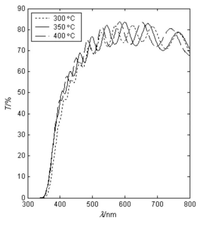
图4 不同基片温度时样品的透射谱Fig.4 Transmittance spectra of the samples deposited with different substrate temperatures
2.2 薄膜的光电性能
图4为不同基片温度时所制备GTZO薄膜的透过率曲线,可以看出,所有薄膜样品的透过率曲线显示了清晰、光滑的干涉条纹,这种透过率曲线的多级振荡来自于薄膜上表面和下表面(即与基片之间的界面)反射光之间的干涉,良好的振荡特性表明所制备的GTZO薄膜具有平整的表面、均匀的厚度和良好的光学质量[36,37].对于图 4 的透过率谱线,可以粗略地分成3个区域:透明振荡区(400~800 nm)、中等吸收区(360~400 nm)和强吸收区(200~360 nm).透明振荡区表明GTZO薄膜在此光谱范围内基本上是透明的.随着波长(λ)减小,GTZO薄膜进入中等吸收区,这时薄膜具有一定的弱吸收能力.当波长λ继续减小时,GTZO薄膜进入强吸收区,可以看到大约在λ=355 nm处,薄膜的透过率急剧下降,其吸收能力显著增强,表明了GTZO薄膜的光学能隙在此附近.图5(a)给出了不同温度时沉积在玻璃基片上GTZO薄膜的平均透过率(Tav,未扣除玻璃基片),当基片温度为300℃,350℃和400℃时,GTZO薄膜/玻璃基片的可见光区平均透过率Tav分别为71.5%,72.6% 和 73.2%,可见,薄膜的平均透过率随着基片温度的升高略有增加,但并没有显著性的变化.图5(b)为GTZO薄膜的方块电阻(Rs)与基片温度之间的变化关系,随着基片温度的升高,方块电阻Rs单调增加,呈现出先平缓而后陡峭的变化趋势.可见,虽然GTZO薄膜的Tav和Rs都随基片温度的升高而增加,但是二者的变化速率却明显不同,因此为了评价透明导电薄膜的光电综合性能,Haacke[38]定义了优良指数,即薄膜的品质因数(FH)为:
公式(2)中,Tav为GTZO薄膜可见光波段的平均透过率,Rs为薄膜的方块电阻[39].不同基片温度下所制备GTZO薄膜样品的品质因数FH如图6所示,基片温度从300℃升高到350℃时,FH增大,而当基片温度继续升高到400℃时,FH反而减小,可见,基片温度为350℃时GTZO薄膜的FH值最大(4.2×10⁻³Ω-1),这表明基片温度为350℃时所制备的GTZO薄膜具有最好的光电综合性能.
2.3 薄膜的光学能隙
由图4可知,GTZO薄膜在波长λ为400~800 nm范围内表现出良好的透光性能,并在355 nm左右有一陡峭的吸收边,在吸收边附近,薄膜的透过率(T)与吸收系数(α)之间满足如下关系式[40]:
公式(3)中,T0和t分别为常数和薄膜厚度.对于吸收边附近有 T0≈1[41],因此,利用式(3)式由薄膜厚度t以及对应的吸收边附近的光学透过率T就可以获得薄膜的光学吸收系数 α.根据 Tauc法则[42],对于薄膜的吸收边附近,光学吸收系数α与入射光子能量(hv)之间满足如下方程:

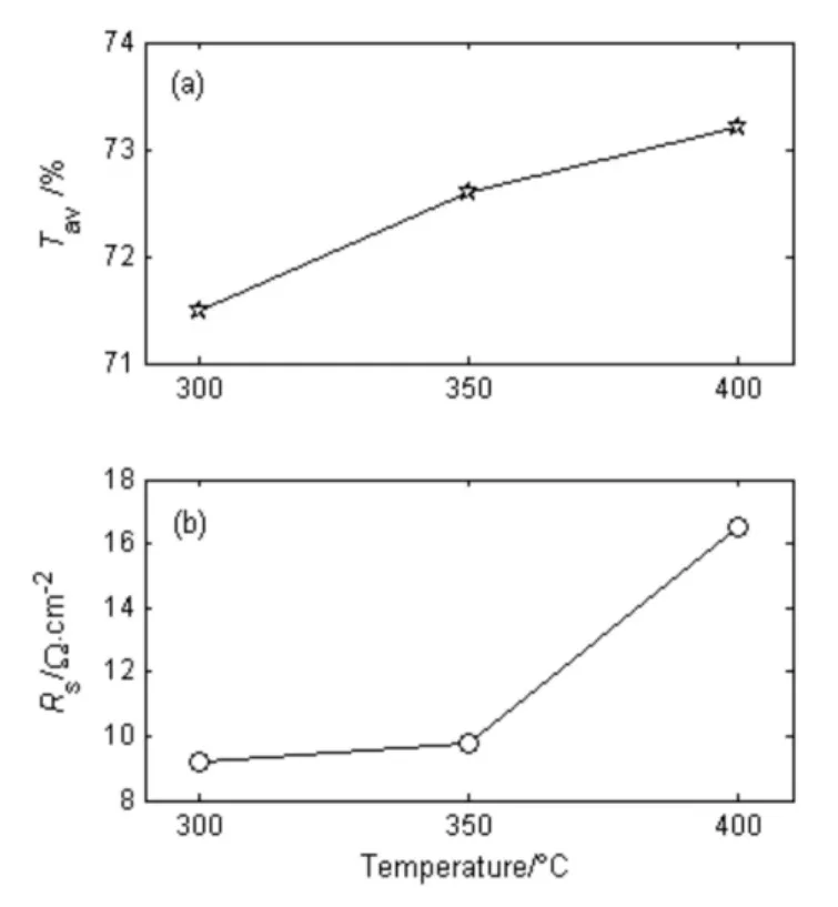
图5 不同基片温度时样品的可见光区平均透过率和方块电阻值Fig.5 Average visible transmittance(Tav)(a)and sheet resistivity(Rs)(b)of the samples deposited with different substrate temperatures
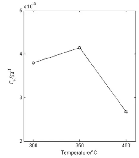
图6 不同基片温度时样品的品质因数Fig.6 Figure of merit for the samples deposited with different substrate temperatures
公式(4)中,C为常数,Eg为薄膜的光学能隙,指数m取决于跃迁的类型.当m=2时,对应于直接跃迁,而当 m=0.5时则对应于间接跃迁[43].由于GTZO薄膜属于直接跃迁,故取m=2作出(αhv)2与hv之间的关系曲线图,根据外推法得到横轴(hv)上的交点(αhv=0)后,容易计算获得薄膜的光学能隙Eg.图7为不同基片温度时所制备GTZO薄膜的(αhv)2-hv关系曲线,利用外推法可得样品的光学能隙Eg值如图8所示,不同基片温度时所制备GTZO薄膜的Eg值为3.48~3.54 eV,均大于纯ZnO薄膜的光学能隙(Eg0=3.37 eV)[8],这主要是 Burstein-Moss(B-M)效应[43,44]所引起的,即由于导带底部附近量子态基本上已被电子占据,故价带中的电子欲想直接跃迁到导带中时,则必须吸收更多的能量才能跃迁到导带中较高的空位上,就如同禁带宽度增加了.GTZO薄膜在紫外光区的吸收是由薄膜中的载流子浓度ne所决定的,由B-M效应而引起的能隙宽化)可以表示为[27,45]:
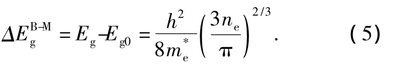
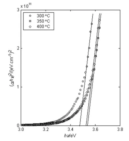
图7 不同基片温度时样品的(αhv)2-hv关系曲线Fig.7 (αhv)2as a function of hv for the samples deposited with different substrate temperatures
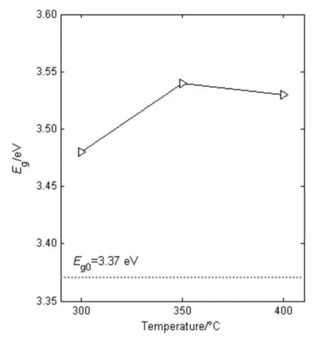
图8 不同基片温度时样品的光学能隙Fig.8 Optical energy gap(Eg)of the samples deposited with different substrate temperatures
3 结语
采用高密度镓钛共掺杂氧化锌铝陶瓷靶作为溅射源,利用射频磁控溅射技术制备了GTZO透明导电薄膜,研究了基片温度对薄膜结构、电学性质和光学性能的影响.实验结果表明:基片温度明显影响GTZO薄膜的晶体结构和光电性能,当基片温度为350℃时,GTZO薄膜具有最好的c轴取向性、最大的晶粒尺寸、较低的方块电阻和较高的可见光区平均透射率,其品质因数最大、光电综合性能最佳.由于受Burstein-Moss效应的影响,所制备GTZO薄膜的光学能隙均大于纯ZnO薄膜的能隙值,同时基片温度对光学能隙也有一定程度的影响,当基片温度为350℃时,GTZO薄膜的光学能隙最大.
[1]Brabec C J.Organic photovoltaics:technology and market[J].Sol Energy Mater Sol Cells,2004,83(2-3):273-292.
[2]Sariciftci N S,Smilowitz L,Heeger A J,et al.Photoinduced electron transfer from conducting polymers onto buckminsterfullerence[J].Science,1992,258(5087):1474-1476.
[3]Yu G,Gao J,Hummelen J C,et al.Polymer photovoltaic cells:enhanced efficiencies via a network ofinternal donor-acceptor heterojunctions[J].Science,1995,270(5243):1789-1791.
[4]Tang C W.Two-layer organic photovoltaic cell[J].Appl Phys Lett,1986,48(2):183-185.
[5]Li G,Shrotriya V,Huang J,et al.High-efficiency solution processable polymer photovoltaic cells by selforganization of polymer blends[J].Nat Mater,2005,4(11):864-868.
[6]Kim J Y,Lee K,Coates N E,et al.Tandem polymer solar cells fabricated by all-solution processing[J].Science,2007,317(5835):222-225.
[7]Chen H Y,Hou J,Zhang S,et al.Polymer solar cells with enhanced open-circuit voltage and efficiency[J].Nat Photonics,2009,3(11):649-653.
[8]Chen H X,Ding J J,Zhao X G,et al.Microstructure and optical properties of ZnO:Al films prepared by radio frequency reactive magnetron sputtering[J].Phys B,2010,405(7):1339-1344.
[9]Jayaraj M K,Antony A,Ramachandran M.Transparent conducting zinc oxide thin film prepared by off-axis rf magnetron sputtering[J].Bull Mater Sci,2002,25(3):227-230.
[10]Sakurai K,Kanehiro M,Nakahara K,et al.Effects of oxygen plasma condition on MBE growth of ZnO[J].J Cryst Growth,2000,209(2-3):522-252.
[11]Cao H T,Pei Z L,Gong J,et al.Transparent conductive Al and Mn doped ZnO thin films prepared by dc reactive magnetron sputtering[J].Surf Coat Technol,2004,184(1):84-92.
[12]Abduev A K,Akhmedov A K,Asvarov A S.The structural and electrical properties of Gd-doped ZnO and Ga,B-codoped ZnO thin films:the effects of additional boron impurity[J].Sol Energy Mater Sol Cells,2007,91(4):258-260.
[13]Aksoy S,Caglar Y,Ilican S,et al.Sol-gel derived Li-Mg co-doped ZnO films: preparation and characterization via XRD,XPS,FESEM[J].J Alloy Compd,2012,512(1):171-178.
[14]Chen J,Chen D,He J,et al.The microstructure,optical,and electrical properties of sol-gel-derived Scdoped and Al-Sc co-doped ZnO thin films[J].Appl Surf Sci,2009,255(23):9413-9419.
[15]袁玉珍,王 辉,张化福,等.膜厚对 Zr,Al共掺杂ZnO透明导电薄膜结构和光电性能的影响[J].人工晶体学报,2010,39(1):169-173.
[16]Nirmala M,Smitha P,Anukaliani A.Optical and electrical properties of undoped and(Mn,Co)codoped ZnO nanoparticles synthesized by DC thermal plasma method[J].Superlattice Microst,2011,50(5):563-571.
[17]Liu Y,Lian J.Optical and electrical properties of aluminum-doped ZnO thin films grown by pulsed laser deposition[J].Appl Surf Sci,2007,253(7):3727-3730.
[18]Shukla R K,Srivastava A,Srivastava A,et al.Growth of transparent conducting nanocrystalline Al doped ZnO thin films by pulsed laser deposition[J].J Cryst Growth,2006,294(2):427-431.
[19]Chen M,Pei Z L,Sun C,et al.ZAO:an attractive potential substitute for ITO in flat display panels[J].Mater Sci Eng B,2001,85(2-3):212-217.
[20]Martin A,Espinos J P,Justo A,et al.Preparation of transparent and conductive Al-doped ZnO thin films by ECR plasma enhanced CVD[J].Surf Coat Technol,2002,151-152(1):289-293.
[21]Heo G S,Gim I G,Park J W,et al.Effects of substrate temperature on propertiesofITO-ZnO composition spread films fabricated by combinatorial RF magnetron sputtering[J].J Solid State Chem,2009,182(10):2937-2940.
[22]Lin Y C,Chen M Z,Kuo C C,et al.Electrical and opticalproperties ofZnO:Alfilm prepared on polyethersulfone substrate by RF magnetron sputtering[J].Colloids Surf A,2009,337(1-3):52-56.
[23]Jeong S H,Park B N,Yoo D G,et al.Al-ZnO thin filmsas transparentconductive oxides:synthesis,characterization,and application tests[J].J Korean Phys Soc,2007,50(3):622-625.
[24]Pei Z L,Zhang X B,Zhang G P,et al.Transparent conductive ZnO:Al thin films deposited on flexible substrates prepared by direct current magnetron sputtering[J].Thin Solid Films,2006,497(1-2):20-23.
[25]Xu Z Q,Deng H,Li Y R,et al.Characteristics of Aldoped c-axis orientation ZnO thin films prepared by the sol-gel method[J].Mater Res Bull,2006,41(2):354-358.
[26]Kim Y S,Tai W P.Electrical and optical properties of Al-doped ZnO thin films by sol-gel process[J].Appl Surf Sci,2007,253(11):4911-4916.
[27]Wang M,Lee K E,Hahn S H,et al.Optical and photoluminescent properties of sol-gel Al-doped ZnO thin films[J].Mater Lett,2007,61(4-5):1118-1121.
[28]Chen H,Guo W,Ding J,et al.Ti-incorporated ZnO films synthesized via magnetron sputtering and its optical properties[J].Superlattice Microst,2012,51(4):544-551.
[29]Jiang M,Liu X,Chen G,et al.Preparation and photoelectric properties of Ti doped ZnO thin films annealed invacuum[J].JMaterSci:Mater Electron,2009,20(12):1225-1228.
[30]Ma Q-B,Ye Z-Z,He H-P,et al.Effects of deposition pressure on the properties of transparent conductive ZnO:Ga films prepared by DC reactive magnetron sputtering[J].Mat Sci Semicon Proc,2007,10(4-5):167-172.
[31]Yang W,Liu Z,Peng D-L,et al.Room-temperature deposition of transparent conducting Al-doped ZnO films by RF magnetron sputtering method[J].Appl Surf Sci,2009,255(11):5669-5673.
[32]Zhang H-F,Liu R-J,Liu H-F,et al.Mn-doped ZnO transparent conducting films deposited by DC magnetron sputtering[J].Mater Lett,2010,64(5):605-607.
[33]Fang G J,Li D,Yao B L.Influence of post-deposition annealing on the properties of transparent conductive nanocrystalline ZAO thin films prepared by RF magnetron sputtering with highly conductive ceramic target[J].Thin Solid Films,2002,418(1):156-162.
[34]Hong R,Shao J,He H,et al.ZnO:Zn phosphor thin films prepared by face-to-face annealing[J].J Cryst Growth,2005,284(3-4):347-352.
[35]Kale R B,Lokhande C D.Influence of air annealing on the structural,opticaland electricalpropertiesof chemically deposited CdSe nano-crystallites[J].Appl Surf Sci,2004,223(4):343-351.
[36]Yadav H K,Sreenivas K,Gupta V.Influence of postdeposition annealing on the structural and optical properties of cosputtered Mn doped ZnO thin films[J].J Appl Phys,2006,99(8):083507-1-083507-8.
[37]Zhong Z-Y,Gu J-H,Sum F-L,et al.Preparation and properties ofgallium-doped zinc oxide transparent conductive thin films[J].J Synth Cryst,2012,41(5):1337-1344.
[38]Haacke G.New figure of merit for transparent conductors[J].J Appl Phys,1976,47(9):4086-4089.
[39]Zhou J,Zhong Z Y.Structural and optoelectrical properties of Ga-doped ZnO semiconductor thin films grown by magnetron sputtering[J].Cryst Res Technol,2012,47(9):944-952.
[40]顾锦华,钟志有,何 翔,等.真空退火处理对光敏薄膜及聚合物太阳电池性能的影响[J].中南民族大学学报:自然科学版,2009,28(3):30-33.
[41]李桂锋,张 群,王颖华,等.高迁移率IWO透明导电氧化物薄膜制备及其退火处理研究[J].真空科学与技术学报,2008,28(2):95-98.
[42]Ratana T,Amornpitoksuk P,Suwanboon S,et al.The wide band gap of highly oriented nanocrystalline Al doped ZnO thin films from sol-gel dip coating[J].J Alloy Compd,2009,470(3):408-412.
[43]孙奉娄,惠述伟.衬底温度对射频溅射沉积ZAO透明导电薄膜性能的影响[J].中南民族大学学报:自然科学版,2009,28(2):10-13.
[44]Prepelita P,Medianu R,Sbarcea B,et al.The influence of using different substrates on the structural and optical characteristics of ZnO thin films[J].Appl Surf Sci,2010,256(9):1807-1811.
[45]Fallah H R,Ghasemi M,Hassanzadeh A,et al.The effect of deposition rate on electrical,optical and structural properties of tin-doped indium oxide(ITO)films on glass at low substrate temperature[J].Phys B,2006,373(1):274-279.
猜你喜欢
材料与冶金学报(2022年2期)2022-08-10
表面技术(2022年3期)2022-03-31
陶瓷学报(2021年5期)2021-11-22
中国品牌(2021年9期)2021-09-14
小天使·一年级语数英综合(2020年5期)2020-12-16
中国造纸(2020年10期)2020-11-04
中国计量大学学报(2019年4期)2019-02-14
环球时报(2018-08-16)2018-08-16
哈尔滨理工大学学报(2014年3期)2015-01-04
汽车电器(2014年8期)2014-02-28