
Enhanced Field Emission Performance and Better Emitting Current Stability of Mixed Multilayer Carbon Nanotube Cathode
2015-12-20 09:13WANGFengge王凤歌LIYukui李玉魁LUWenke卢文科
关键词:文科
WANG Feng-ge (王凤歌),LI Yu-kui (李玉魁)* ,LU Wen-ke (卢文科)
1 School of Electronic Information,Zhongyuan Institute of Technology,Zhengzhou 450007,China
2 School of Information Science and Technology,Donghua University,Shanghai 200051,China
Introduction
Carbon nanotubes (CNTs)possessed attractive properties for field emission material,such as high mechanical strength,superior chemical stability,small radius of curvature,and promising electron emission capability[1-5].With CNTs as excellent field emitters,the field emission displays (FEDs)had been extensively studied in recent years.In cathode,the CNTs were commonly attached onto the cathode electrode surface to form the CNT cathode,which also was the favorable electron source[6-8].However,because of the lack of a stable fabrication technology,the development of CNT cathode had been limited.For the cathode that the CNTs were printed on the electric dielectric layer,the better field emission uniformity had been confirmed,but the adhesion performance of CNT was poor,and the manufacture cost was too high.That the CNTs were fabricated on the metal layer to form the cathode was a preferable blue print,and the better field emission performance was also improved.Nevertheless,its fabrication process was complex and the electrical contact property was also not satisfactory.For the cathode that the CNTs were grown directly on the silicon wafer,and the better field emission ability could be achieved.But the large-area cathode fabrication was impossible,and it was also not suitable for the patterned fabrication of FED cathode[9-15].With regard to the cathode fabrication method,the screen printing technique,which was an effective and low cost process,had been widely adopted.However,some drawbacks for this transplanted CNT layer should be overcome.For example, the field emission characteristics were worse because the CNTs were randomly distributed;the printed CNTs were dropped off easily from the cathode electrode surface,so that the field emitters would become invalid[16-18].Therefore,the research on the fabrication of a high performance CNT cathode would continue to conduct,and a low-cost CNT cathode fabrication was also the prerequisite of FED practical application[19-21].For solving the abovementioned difficult problem,a new mixed multilayer CNT cathode was reported in this paper.The middle CNT layer was used as a buffer layer between the top CNT layer and the ZnO layer.The high temperature sintering treatment was utilized to enhance the field emission characteristics.The ZnO layer fabricated on the bottom electrode surface and the ZnO nanoparticles was adopted to adjust the electron emission current.The mixed multilayer CNT cathode FED was fabricated,and the green luminescence image with high-quality was also demonstrated,which proved that the mixed multilayer CNT cathode possessed better field emission performance.
1 Experimental
1.1 Design of mixed multilayer CNT cathode
A structural schematic diagram of mixed multilayer CNT cathode was given in Fig.1.The mixed multilayer CNT cathode was fabricated on cathode glass plate,which was formed with the cut soda lime flat glass.For one mixed multilayer CNT cathode,five parts were included,which were the bottom electrode,the ZnO layer,the separating layer,the middle CNT layer,and the top CNT layer,respectively.The separating layer was fabricated with the sintered insulation slurry,which was used to separate the different mixed multilayer CNT cathodes.Good electric connection should be performed between the ZnO layer and the bottom electrode,which are together served as the cathode electrode.The prepared CNT layer,which included the top CNT layer and the middle CNT layer,was utilized to supply electrons for FED.

Fig.1 Structural schematic diagram of mixed multilayer CNT cathode
1.2 Fabrication process
Firstly,the top CNT layer paste and the middle CNT layer paste were prepared separately.In this study,the double-walled CNT was adopted,in which the length of CNT was approximate 15-25 μm.For top CNT paste,the purified CNT,the ethyl cellulose,and the terpineol were mixed to form the top CNT layer mixture slurry.The top CNT layer mixture slurry was heated to 76 ℃,and was stirred with the magnetic stirrer to form the top CNT layer paste.For middle CNT layer paste,the purified CNTs and the ZnO powder which were composed of much ZnO nano-particles in fact,were mixed.After the terpineol solution was added,a well-dispersing process with supersonic oscillations was performed to form the middle CNT layer mixture slurry.The middle CNT layer mixture slurry was heated to 125 ℃,and then the ethyl cellulose was blended.After sufficient stirring process,the middle CNT layer paste was formed.Secondly,the indium tin oxide film covering on cathode glass plate was divided to form the bottom electrodes.The width of one bottom electrode was 380 μm and electric insulation should be performed between the different bottom electrodes.The insulation slurry was fabricated on cathode glass plate,and the solidified insulation slurry was used to form the black separating layer.Thirdly,the ZnO slurry was fabricated on the bottom electrode surface.The baking process was conducted in an automatic electric oven,in which the baking temperature was 185 ℃and the baking time was 30 min.Then the sintering process for baked ZnO layer was performed in the special sintering furnace,in which the maximum sintering temperature was 540 ℃and the holding time at the maximum sintering temperature was 5 min.The total sintering time was about 70 min.Finally,the middle CNT layer paste was screenprinted on the ZnO layer surface.A baking process was conducted,in which the baking temperature was 265 ℃.Then,the top CNT layer paste was fabricated on baked middle CNT layer surface.The baking process was also performed,in which the baking temperature was about 240℃ and the baking time was 30 min.In special CNT sintering furnace,the baked middle CNT layer paste and top CNT layer paste were sintered simultaneously.For avoiding that the CNT was oxidized in the sintering course,the argon (the purity was 99.99%)was used as the protective gas.The maximum sintering temperature was 530 ℃ and the maintaining time at the maximum sintering temperature was 10 min.After being cooled to the room temperature,the middle CNT layer and the top CNT layer were formed.After the proper post-treatment process,the mixed multilayer CNT cathode was fabricated.
1.3 Packaging of mixed multilayer CNT cathode FED prototype
The cathode glass plate,the glass frame,and the anode glass plate combined to make a vacuum chamber.The sintered glass frit was used to seal the whole vacuum chamber.So the mixed multilayer CNT cathode FED prototype was fabricated.To compare the influence of different CNT cathode on the field emission characteristics,the CNT was prepared directly on the bottom electrode to form the usual cold cathode.With a similar manufacture process,the other kind of usual cold cathode FED was also fabricated.
2 Results and Discussion
2.1 SEM photos of CNT surface morphology
In Fig.2,the scanning electron microscope (SEM)photo s of the surface morphology for CNT in mixed multilayer CNT cathode were illustrated.Thereinto,the SEM photo of baked CNT was given in Fig.2(a).As could be seen from the photo,lots of CNT was adhered with the nubbly organic slurry.Most of CNT ends were covered,even many CNTs were buried entirely in the CNT layer paste.It was impossible for the normal electron emission because the CNT could not protrude from the CNT layer surface.The SEM photo of treated CNT was presented in Fig.2(b).Seen from the photo,several gained results were as follows.(1)The blocks of organic slurry had been removed.In the sintering course,the maximum sintering temperature of 530℃was adopted.Under so high temperature,not only would the organic binding material be vaporized completely,but also the organic contaminants in CNT paste were also sintered.(2)An even and clean CNT layer surface appeared,and potential field emission sites had been formed.In our experiment,the holding time of 10 min at the maximum sintering temperature was utilized,in which the purpose was to carry out the sintering course more thoroughly.Due to the existing of protective gas,the CNT could not also be oxidized.For the even CNT layer surface,it was beneficial that the uniform electron emission could be ensured.And for the much field emission sites,it was also advantageous to form a larger electron emission current.(3)The CNT was stuck firmly on the mixed multilayer CNT cathode surface,and the discrete ZnO nano-particle was not observed.In the cathode preparation process,the ZnO layer was fabricated on the bottom electrode surface.For improving the electron emission performance and the adhesion capability of CNT,the middle CNT layer was used as a buffer layer between the top CNT layer and the ZnO layer.On one hand,parts of CNTs in the middle CNT layer could be fixed easily on the ZnO layer due to the existing of ZnO nano-particles in the high temperature sintering treatment course;the CNTs in top CNT layer could also permeate the middle CNT layer.With the twine each other of different CNTs,it was natural that the adhesion capability of CNT upon the ZnO layer was strengthened.On the other hand,the top CNT layer was fabricated on the middle CNT layer surface,so the ZnO nano-particles were covered.It was ensured that the emitted electrons in the mixed multilayer CNT cathode FED would derive from the CNT entirely.
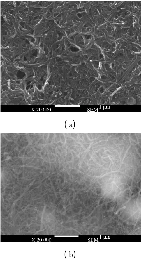
Fig.2 The SEM photo of surface morphology for (a)baked CNT and(b)treated CNT
2.2 Field emission characteristics
The typical field emission characteristic curves were presented in Fig.3.Thereinto,the curve (a)showed field emission property of the mixed multilayer CNT cathode FED,while the curve (b)demonstrated the one of usual cold cathode FED.The operating voltages were applied with the direct current(DC)power supply,and the emission current was monitored with the ammeter.Seen from the curves,several obvious results could be obtained.(1)On the whole,all the kinds of FEDs possessed good field emission characteristics.It was not surprised because the cathode material was composed of CNTs.The electrons could be emitted normally from the CNT layer,which would indicate that the fabrication of mixed multilayer CNT cathode was feasible.In addition,the mixed multilayer CNT cathode FED had lower turn-on electric field.The turn-on electric field of usual cold cathode FED was about 1.99 V/μm,and the one of mixed multilayer CNT cathode FED was approximate 1.79 V/μm.(2)By comparing with the usual cold cathode FED,the mixed multilayer CNT cathode FED had superior electron emission performance.For example,under the same electric field of 2.25 V/μm,the electron emission current of mixed multilayer CNT cathode FED was 365 μA,while the one of usual cold cathode FED was only 171 μA.On the contrary,with the same electron emission current of 690 μA,the necessary electric field was 2.9 V/μm for usual cold cathode FED,which would be larger than the one of 2.69 V/μm for mixed multilayer CNT cathode FED.The maximum electron emission current of the mixed multilayer CNT cathode FED was about 2 675 μA,which would exceed the one of usual cold cathode FED (was approximate 2 056 μA).We think that the mixed multilayer CNT cathode played an important part in the field emission course for enhancing the electron emission current of whole FED.(3)However,it was worthwhile to notice that the increasing range of electron emission current in the two kinds of FEDs was different.For example,when the electric field was enhanced from 2.93 V/μm to 3.13 V/μm,the increment of electron emission current for mixed multilayer CNT cathode FED was about 878 μA,and the one for usual cold cathode FED was approximate 1 058 μA.In other words,it seemed that the field emission curve of usual cold cathode FED was much steep.Nevertheless,it was not strange that the increment of electron emission current for mixed multilayer CNT cathode FED was less than the one for usual cold cathode FED,just because the ZnO layer and the ZnO nano-particles in middle CNT layer would begin to adjust the electron emission current.Both the ZnO layer and the ZnO nano-particles in middle CNT layer were not only the cathode electrode but also the current-limiting layer.As a cathode electrode,the cathode potential could be conducted smoothly to the CNT;as a current-limiting layer,the abrupt increased peak current of CNT cathode could be effective restrained.This was also why the variation trend of field emission curve for the mixed multilayer CNT cathode FED was some slow.In spite of this,it was beneficial to the whole triode FED with the fabricated ZnO layer and ZnO nano-particles in middle CNT layer.For example,the CNT tip shielding effect was eliminated,the emission current stability was enhanced,and the luminescence image uniformity was improved remarkably.
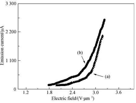
Fig.3 Field emission characteristic for (a)the mixed multilayer CNT cathode FED and (b)the usual cold cathode FED
2.3 Ageing testing
The ageing testing characteristic curves for two kinds of FEDs were presented in Fig.4.In fact,the ageing testing was a necessary course for electronic product,in which the research on the changing of field emission property with repeating measuring for the same FED prototype would be conducted.In the ageing testing course,the unqualified FED would be eliminated,and the unsuitable fabrication process would also be corrected.The measured characteristic curves for mixed multilayer CNT cathode FED were shown in Fig.4(a),and the one for usual cold cathode FED was given in Fig.4(b).The applied external conditions for the two kinds of FEDs in the testing course were identical,in which the applied anode operating voltage was 1.65 kV.The time interval between the two testing course was 48 h.
As could be seen from the Fig.4(a),the second time measuring curve,by comparing with the first time measuring curve,was almost overlapped together.All in all,the electron emission current difference in the two testing course with the same testing condition was small,and even some measuring data were identical.Not only for the curve variation trend and the turn-on electric field but also for the electron emission current variation range and the electron emission current increment,there were not significant changes.It would indicate that the mixed multilayer CNT cathode FED possessed better ageing properties.For mixed multilayer CNT cathode,after the high temperature sintering treatment,the CNTs were fixed solidly on the ZnO layer surface.In other words,the electric contact between the CNT and the ZnO layer could be enhanced.Because parts of CNTs had been embedded in the solidified ZnO layer,the electric contact in the ageing testing course would not also change dramatically.In Fig.4(b),under the identical testing condition,the difference of electron emission current in the two testing course was large,and the two age testing characteristic curves had been separated obviously.For usual cold cathode,the CNT was attached upon the bottom electrode surface.So the electric contact resistance was varied under different usual cold cathode pixels.Furthermore,in the ageing testing course,some residual organic binding material was burned out under the effecting of large electron emission current.Although the turn-on electric field was not differed,the electron emission current variation range had been changed,especially in large electron emission current circumstances.As some residual organic binding material would disappear,it was not surprised that the electric contact resistance in different cathode pixels would be varied.So for usual cold cathode FED,the ageing testing course was necessary.Only after many times and repeated ageing testing,the field emission characteristic of usual cold cathode FED would become stabilize.In mixed multilayer CNT cathode FED,because of the high temperature sintering treatment,the better electric contact had been formed,which was helpful for enhancing the field emission property of whole FED.

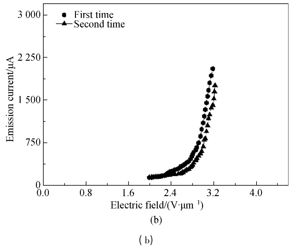
Fig.4 Ageing testing characteristic curves for (a)the mixed multilayer CNT cathode FED and (b)the usual cold cathode FED
For the mixed multilayer CNT cathode FED,on one hand,it's not necessary for the ageing testing course to improve the electron emission current stability,which was beneficial for reducing the manufacture process and the fabrication cost.On the other hand,the electron emission uniformity of CNT would also become better owing to the good electric contact.For disposing of the organic binding material in CNT paste,the high temperature sintering treatment was a high effective process.Firstly,most of organic binding material and other impurity would gradually disappear because they could not suffer the high temperature.And any remnant would also not exist.Secondly,it need not have directly contact with the CNT layer.Not only could the CNT layer surface not be damaged by external mechanical forces, but also the other foreign residue contamination would be generated.Thirdly,the process was more suitable for the fabrication of large-area CNT cathode.The treatment course was relatively simple and the treatment cost was also low.Furthermore,the process temperature was compatible with the standard glass plate.
2.4 Emission image
The typical emission images were given in Fig.5.The green luminescence photo was taken with digital camera,and the luminescence testing was carried out in our experiment platform.

Fig.5 Emission image of mixed multilayer CNT cathode FED
Seen from the given emission image,several significative results could be achieved.(1)The emission image could be displayed normally.It would indicate that the fabrication process of mixed multilayer CNT cathode was feasible.It was not difficult to imagine that the FED emission image would not be formed if the fabricated mixed multilayer CNT cathode could not supply lots of electrons.Not only was the manufacture process of mixed multilayer CNT cathode simple,but also the fabrication cost was low.It possessed considerable potential for practical application.(2) The luminescence brightness uniformity of emission image for mixed multilayer CNT cathode FED was improved.All the anode pixels in anode glass plate could be lightened,and the difference of emission image luminescence brightness for different anode pixels was slight.In mixed multilayer CNT cathode,the ZnO layer,together with the ZnO nano-particle in the solidified middle CNT layer,would adjust the formed electron emission current automatically.That would improve the whole emission image luminescence brightness uniformity of mixed multilayer CNT cathode FED.(3)The whole luminescence brightness of emission image for mixed multilayer CNT cathode FED was high.The nonluminous anode pixels had not been observed.On one hand,it showed that the electrons had been emitted from the CNT of mixed multilayer CNT cathode in the field emission form.With the treatment of high temperature sintering and the fabrication of top CNT layer,the electrons only could be derived from the CNT,rather than other impurity.On the other hand,due to the better electric conduction performance of bottom electrode and ZnO layer,the cathode potential could be transmitted to the CNT smoothly.So the CNT could supply more electrons,which was also a powerful guarantee for enhancing the luminescence brightness of emission image for mixed multilayer CNT cathode FED.
Figure 6 revealed the curve of luminescence brightness vs.electric field for the mixed multilayer CNT cathode FED.In the measuring course,the applied anode potential was fixed,which was 1.72 kV.The maximum luminescence brightness had reached 1 832 cd/m2.
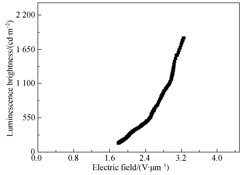
Fig.6 The luminescence birghtness of mixed multilayer CNT cathode FED
2.5 Real photograph of FED
The real photograph of mixed multilayer CNT cathode FED prototype was shown in Fig.7.Because of the covering of anode insulation layer,the mixed multilayer CNT cathode was invisible.After the external operation potential including the anode voltage and the grid voltage were applied,the electron beam originated from the mixed multilayer CNT cathode would be formed,which was the basic that the FED prototype could generate visible light.The anode pixels were fabricated on the anode glass plate in a 7(row)×22(column)matrix form.So there were 154 anode pixels in number,which could display some simple dot matrix character images with the helping of drive circuit.The one anode pixel was square shape,and all the 7 ×22 anode pixels with green phosphor layer were identical in fabrication size.
In the production process,the CNT had experienced several relatively high temperature cycles,which might include the high temperature sintering treatment course,the sintering process of low-melting glass frit,and the heating exhaust process.However,the CNTs in the mixed multilayer CNT cathde would not be impaired,which would be proved that the whole FED prototype could operate normally.The gas in the vacuum chamber would be evacuated out through the exhaust tube.Of course,the air leak would not be permitted for the fullsealed vacuum chamber.The activated getters,which could be seen in Fig.7,were utilized to maintain the high vacuum environment,which would ensure that the mixed multilayer CNT cathode FED could work for a long time.

Fig.7 The real photograph of a mixed multilayer CNT cathode FED prototype
3 Conclusions
A new mixed multilayer CNT cathode was developed firstly on cathode glass plate.The high temperature sintering treatment was utilized for enhancing the field emission characteristics.The middle CNT layer was fabricated as a buffer layer between the top CNT layer and the ZnO layer,which was used to improve the electron emission capability and adhesion performance of CNT.The ZnO layer,which was fabricated on the bottom electrode surface,and the ZnO nano-particles were adopted,by which the electron emission current could be adjusted.The fabrication of mixed multilayer CNT cathode was simple with low manufacture cost.With the mixed multilayer CNT cathode,a triode FED prototype was fabricated,which demonstrated good field emission properties and better ageing test characteristics.The good luminescence image brightness uniformity was also achieved, in which the maximum luminescence image brightness had reached 1 832 cd/m2.These fabrication processes and proposed manufacture structure appeared to possess high potential in practical applications.
[1]Lee H,Goak J,Choi J,et al.High-Current Field Emission of Point-Type Carbon Nanotube Emitters on Ni-coated Metal Wires[J].Carbon,2012,50(6):2126-2133.
[2]Lee Y D,Cho W S,Kim Y C,et al.Field Emission of Ribonucleic Acid-Carbon Nanotube Films Prepared by Electroporetic Deposition[J].Carbon,2012,50(3):845-850.
[3]Lee S F,Chang Y P,Lee L Y.Synthesis of Carbon Nanotubes on Silicon Nanowires by Thermal Chemical Vapor Deposition[J].New Carbon Materials,2011,26(6):401-407.
[4]Giubileo F,Bartolomeo A D,Sarno M,et al.Field Emission Properties of As-Grown Multiwalled Carbon Nanotube Films[J].Carbon,2012,50(1):163-169.
[5]Mathur A,Roy S S,Hazra K S,et al.Oxygen Plasma Assisted End-Opening and Field Emission Enhancement in Vertically Aligned Multiwall Carbon Nanotubes[J].Materials Chemistry and Physics,2012,134(1):425-429.
[6]Li Y K,Li X Q,Liu X H,et al.Fabrication Research and Property of Enhanced Petaling Cold Cathode with Carbon Nanotube[J].Journal of Donghua University,2013,30(2):10-13.
[7]Lee J,Jung Y,Song J,et al.High-Performance Field Emission from a Carbon Nanotube Carpet[J].Carbon,2012,50(10):3889-3896.
[8]Li Y K,Li X Q,Liu X H,et al.Fabrication Research on the Sandwich Layered Cathode Electrode for a Triode Field Emission Display Prototype[J].Journal of Semiconductors,2013,34(7):074004-1-6.
[9]Lee S H,Ma C C M,Yuen S M,et al.Magnetic Field Enhances the Graphitized Structure and Field Emision Effect of Carbon Nanotubes[J].Thin Solid Films,2011,519(13):4166-4173.
[10]Hojati-Talemi P,Kannan A G,Simon G P.Fusion of Carbon Nanotubes for Fabrication of Field Emission Cathodes [J].Carbon,2012,50(2):356-361.
[11]Wu H C,Youh M J,Lin W H,et al.Fabrication of Double-Sided Field-Emission Light Source Using a Mixture of Carbon Nanotubes and Phosphor Sandwiched between Two Electrode Layers[J].Carbon,2012,50(13):4781-4786.
[12]Zajec B,NemanicˇV,Žumer M,et al.Ring-Shaped Field Emission Patterns from Carbon Nanotube Films [J].Carbon,2011,49(10):3332-3339.
[13]Aykut Y.Electrospun MgO-Loaded Carbon Nanofibers:Enhanced Field Electron Emission from the Fibers in Vacuum[J].Journal of Physics and Chemistry of Solids,2013,74(2):328-337.
[14]Yuge R,Toyama K,Ichihashi T,et al.Characterization and Field Emission Properties of Multi-walled Carbon Nanotubes with Fine Crystallinity Prepared by CO2Laser Ablation[J].Applied Surface Science,2012,258(18):6958-6962.
[15]Lahiri I,Verma V P,Choi W.An All-Graphene Based Transparent and Flexible Field Emission Device [J].Carbon,2011,49(5):1614-1619.
[16]Yoon D H,Choi Y C.Improved Field Emission Stability and Uniformity of Printed Carbon Nanotubes Prepared Using High Energy-Milled Glass Frit[J].Current Applied Physics,2013,13(7):1477-1481.
[17]Futaba DN,Kimura H,Zhao B,et al.Carbon Nanotube Loop Arrays for Low-Operational Power, High Uniformity Field Emission with Long-Term Stability[J].Carbon,2012,50(8):2796-2803.
[18]Bae N Y,Bae W M,Ha A N,et al.Low-Voltage Driven Carbon Nanotube Field Emission Lamp [J].Current Applied Physics,2011,11(4):S86-S89.
[19]Jung H,An S Y,Jang D M,et al.A Multi-wall Carbon Nanotube/Polymethyl Methacrylate Composite for Use in Field Emitters on Flexible Substrates [J].Carbon,2012,50(3):987-993.
[20]Neupane S,Lastres M,Chiarella M,et al.Synthesis and Field Emission Properties of Vertically Aligned Carbon Nanotube Arrays on Copper[J].Carbon,2012,50(7):2641-2650.
[21]Cho W S,Lee Y D,Choi J,et al.Effects on the Field Emission Properties by Variation in Surface Morphology of Patterned Photosensitive Carbon Nanotube Paste Using Organic Solvent[J].Applied Surface Science,2011,257(6):2250-2253.
猜你喜欢
北京林业大学学报(社会科学版)(2022年4期)2023-01-04
社会科学战线(2022年4期)2022-06-15
中学生博览·文艺憩(2020年3期)2020-08-14
求学·文科版(2019年6期)2019-06-12
艺术家(2018年7期)2018-09-22
求学·文科版(2018年7期)2018-05-14
数学学习与研究(2018年5期)2018-03-28
东方艺术·国画(2016年1期)2016-11-16
黄河之声(2016年18期)2016-02-07
 Journal of Donghua University(English Edition)2015年3期
- Journal of Donghua University(English Edition)的其它文章
- Evaluation of Cadmium Bioavailability in Soils Using Diffusive Gradients in Thin Film Technique and Traditional Methods
- Structured Query Language Injection Penetration Test Case Generation Based on Formal Description
- Graph Regularized Sparse Coding Method for Highly Undersampled MRI Reconstruction
- Application of Monetary Unit Sampling Based on Extended Audit Game
- Group Performance Evaluation in Universities with Entropy Method
- On Augmented Zagreb Index of Molecular Graphs